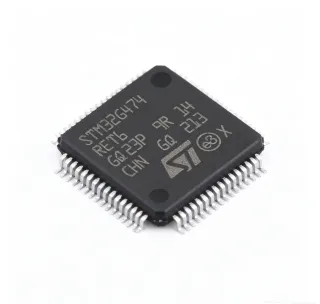
STM32F103RBT6 - 72MHz Cortex-M3 MCU 128KB Flash | ST
MPN: STM32F103RBT6 ✓ Active| Qty | Unit Price | Extended |
|---|---|---|
| 1 | $5.2 | $5.20 |
| 10 | $4.68 | $46.80 |
| 100 | $4.16 | $416.00 |
| 500 | $3.74 | $1,870.00 |
| 1,000 | $3.32 | $3,320.00 |
STM32F103RBT6 Overview
A microcontroller unit (MCU) is a single integrated circuit that combines a processor core, memory, and programmable peripherals into one device, forming the lowest layer of the embedded-system hierarchy: MCU -> microcontroller -> embedded processor -> system-on-chip. The ARM Cortex-M3 is a 32-bit RISC processor core optimized for cost-sensitive and power-conscious embedded control, and the STM32F103 family was one of the first mainstream Cortex-M families adopted at scale across industrial electronics.
Key features include the 72 MHz Cortex-M3 core with a 1.25 DMIPS/MHz performance rating, 128 KB of on-chip Flash with a single-bank architecture, 20 KB of SRAM, an 8 MHz or 16 MHz external crystal option with an internal 8 MHz HSI RC oscillator, and a 2.0 V to 3.6 V supply range with a 2.5V/3.3V operating point. Peripherals include two SPI, two I2C, three USART, one USB full-speed interface, one CAN 2.0B controller, and a 12-bit ADC delivering up to 1 microsecond conversion time.
Architecturally, the device uses an ARMv7-M Harvard structure with a three-stage pipeline and a Nested Vectored Interrupt Controller (NVIC) providing low-latency interrupt response. The AHB/APB bus matrix lets peripherals run concurrently with core execution, while the Flash accelerator minimizes stalls from the 72 MHz core fetching from Flash.
Typical applications include industrial control nodes, motor-control auxiliary boards, USB and CAN communication modules, low-cost development platforms, and legacy 8-bit/16-bit MCU upgrades where the ARM tool ecosystem reduces software cost.
Design consideration: pin compatibility across the STM32F1 family means Flash upgrades from 128 KB to 256 KB (STM32F103RCT6) require no PCB change, but verify RAM sizing and the 72 MHz maximum frequency when porting from faster derivative families.
This page synthesizes distributor pricing, verified drop-in alternatives including GD32F103 and APM32F103 second sources, and practical design notes not found in the manufacturer datasheet.
Drop-in alternatives for STM32F103RBT6 — same package, pin-to-pin compatible. Different-package parts requiring PCB rework are excluded.
Variants in this series
Same-series models that are drop-in compatible with STM32F103RBT6 (same form factor and footprint) — differing in Package, Flash Memory, SRAM, Timers, Core Processor.
Quick Comparison Tool — Select alternative parts for side-by-side comparison:
STM32F103RCT6
✅ Drop-In ⚠️ 参数待验证✓ In Stock
$3.35 / Unit
View Datasheet →STM32F103RBT7
✅ Drop-In ⚠️ 参数待验证📋 Reference alternative (not in catalog)
GD32F103RBT6
✅ Drop-In📋 Reference alternative (not in catalog)
APM32F103RBT6
✅ Drop-In📋 Reference alternative (not in catalog)
AT32F403ARBT7
✅ Drop-In📋 Reference alternative (not in catalog)
CKS32F103RBT6
✅ Drop-In📋 Reference alternative (not in catalog)
STM32F103RBT6 Maximum Ratings & Electrical Characteristics
| Core Processor | ARM Cortex-M3 |
| Core Size | 32-bit |
| Maximum Clock Frequency | 72 MHz |
| Flash Memory Size | 128 KB (128K x 8) |
| RAM Size | 20 KB |
| Supply Voltage | 2.5 V / 3.3 V |
| Package | LQFP-64 (10x10 mm) |
| Mounting Type | Surface Mount |
| Peripherals | USB, CAN, DMA, PWM, WDT |
| Connectivity | CANbus, I2C, SPI, UART/USART, USB |
| Timers | Seven 16-bit timers |
| Packaging | Tray |
| Program Memory Type | FLASH |
STM32F103RBT6 lqfp-64 (10x10 mm) Pin Configuration Guide
Pin configuration for STM32F103RBT6 (lqfp-64 (10x10 mm) package). This digital IC includes GPIO, communication interfaces (UART, SPI, I2C), and power pins. Refer to the manufacturer datasheet for alternate pin functions and configuration options. Essential for embedded system design and PCB layout.

No detailed pinout data available for STM32F103RBT6.
Refer to the datasheet for full pin configuration.
Typical Applications
STM32F103RBT6 is suitable for 6 applications: Industrial Control Nodes, USB Communication Modules, Motor Control Auxiliary Boards, Low-Cost Development Platforms, Legacy 8/16-bit MCU Upgrades, IoT Sensor Gateways.
Industrial Control Nodes
The STM32F103RBT6 fits industrial control and automation nodes where a 72 MHz Cortex-M3, 128 KB Flash, and rich timer resources are sufficient without the cost of higher-performance MCUs. Its seven 16-bit timers support PWM generation for actuator drives, while the CAN 2.0B controller natively interfaces with industrial fieldbuses such as CANopen. In a typical node, the MCU polls sensors over I2C/SPI, executes control loops, and reports status over CAN at 1 Mbps; the 20 KB SRAM comfortably buffers communication frames. Design consideration: use the independent watchdog and Brown-Out Reset for fail-safe operation in electrically noisy factory environments.
Recommended
USB Communication Modules
With an integrated USB 2.0 full-speed device controller, the STM32F103RBT6 is a classic choice for USB CDC virtual-serial bridges, HID devices, and custom-class data loggers. The 12 Mbps full-speed link pairs naturally with the three USARTs, letting the MCU translate USB traffic to RS-232/RS-485 PHYs. ST's USB device library provides ready CDC/HID/MSC class stacks that fit well within 128 KB Flash. Design notes: derive the precise 48 MHz USB clock from an external 8 MHz crystal via PLL, and place the 1.5 kOhm D+ pull-up correctly - many first-revision boards fail enumeration because this resistor is driven from the wrong GPIO timing.
Recommended
Motor Control Auxiliary Boards
For motor-control auxiliaries - gate-driver interface boards, encoders, and supervisory controllers - the STM32F103RBT6 offers advanced timers with complementary PWM outputs and dead-time insertion, plus a 12-bit ADC with fast conversion for current-sense feedback. The 72 MHz core executes FOC-lite or trapezoidal commutation supervision while the DMA offloads ADC sampling. Mounting it on the same LQFP-64 footprint as the STM32F103RCT6 lets one PCB serve both low- and high-memory firmware variants. Thermal-wise, dissipation is low (tens of mA at 72 MHz), so a modest copper pour suffices; focus layout effort on short, Kelvin-routed current-shunt traces to the ADC.
Recommended
Low-Cost Development Platforms
The STM32F103RBT6 underpins countless low-cost development boards and educational platforms because the ARM Cortex-M3 ecosystem - STM32CubeIDE, Keil, GCC toolchains, and ST-Link debugging - is free or inexpensive and heavily documented. Its 128 KB Flash leaves ample room for bootloader plus application, and the SWD interface needs only four pins, simplifying board design. University labs and maker products favor it for teaching embedded C, interrupt-driven design, and RTOS basics. Note for new designs: ST positions the STM32F1 as a mature series; for greenfield projects needing modern peripherals, compare against STM32G0/G4, but for ecosystem continuity and low-cost clone-compatible supply, the F103 remains pragmatic.
Recommended
Legacy 8/16-bit MCU Upgrades
When replacing legacy 8-bit or 16-bit MCUs, the STM32F103RBT6 provides a 32-bit upgrade path at a comparable cost point: 1.25 DMIPS/MHz performance, a mature C compiler ecosystem, and a peripheral set (UART, SPI, I2C, timers) that maps cleanly onto legacy register-level code after porting. The 128 KB Flash typically holds the legacy application with room for future features, and the 2.0V-3.6V supply integrates into existing 3.3V or 5V-with-regulator designs. Migration tip: start from ST's standard peripheral library rather than bare-register ports to reduce bring-up risk, and take advantage of the bit-banding region for legacy code that relies on atomic bit manipulation.
Recommended
IoT Sensor Gateways
As a gateway MCU for IoT sensor clusters, the STM32F103RBT6 aggregates multi-sensor data over its two I2C and two SPI buses, preprocesses it with the 72 MHz core, and forwards it via UART to a wireless module (LoRa, NB-IoT, or Wi-Fi). The 128 KB Flash accommodates protocol stacks, local buffering in 20 KB SRAM, and field-updatable firmware with a dual-image bootloader. Its broad availability and pin-compatible second sources (GD32F103RBT6, APM32F103RBT6) de-risk long-life IoT deployments against supply disruption. For battery-powered nodes, leverage the STM32F1 stop mode (microamp-class currents) and wake on RTC or external interrupts.
Recommended
Recommended Products Summary
Engineering reference data for STM32F103RBT6 — comparison, design guidance, and compliance information.
Selection Guide
Comparison with Alternatives
| Parameter | This Product | STM32F103RCT6 | GD32F103RBT6 | APM32F103RBT6 | AT32F403ARBT7 |
|---|---|---|---|---|---|
| Brand | STMicroelectronics | STMicroelectronics | GigaDevice | Geehy Semiconductor | Artery Technology |
| Package | LQFP-64 | LQFP-64 - same footprint | LQFP-64 - same footprint | LQFP-64 - same footprint | LQFP-64 - same footprint |
| Core / Max Frequency | Cortex-M3, 72 MHz | Cortex-M3, 72 MHz | Cortex-M3, up to 108 MHz | Cortex-M3, 72 MHz class | Cortex-M4, up to 200 MHz |
| Flash Memory | 128 KB | 256 KB | 128 KB | 128 KB | 192 KB (expandable) |
| RAM | 20 KB | 48 KB | 20 KB | 20 KB | 36 KB+ |
| USB / CAN | USB FS + CAN 2.0B | USB FS + CAN 2.0B | USB FS + CAN 2.0B (compatible) | USB FS + CAN 2.0B (compatible) | USB FS + CAN 2.0B (compatible) |
| STM32F1 Register Compatibility | Native | Native (same family) | High (documented second source) | High | High, with enhanced peripherals |
Key Differentiators
- Double the memory without a PCB change (vs STM32F103RCT6)
- Ecosystem maturity over domestic second sources (vs GD32F103RBT6)
- Lower architectural risk than upgrade-path parts (vs AT32F403ARBT7)
Design Notes
Decouple every VDD pin with a 100 nF ceramic capacitor placed within 5 mm of the pin, plus one 4.7-10 uF bulk capacitor near the device. VDDA must be filtered separately - a ferrite bead followed by 1 uF + 10 nF is the standard ST reference-design pattern - because ADC accuracy degrades sharply with VDDA ripple. Estimated: at 72 MHz with all peripherals active, typical supply current is roughly 50 mA, so a 3.3V rail rated for 150 mA provides comfortable margin.
Break out the SWD header (SWCLK, SWDIO, GND, 3.3V, NRST) on every production board even if field programming is not planned - it costs four test points and saves the board from being unflashable after a bootloader mistake. Route SWD traces short and away from switching nodes. BOOT0 must be strapped to GND through a 10 kOhm resistor; never leave it floating, as float conditions can cause the device to enter the system bootloader instead of running Flash firmware.
The most common STM32F103 pitfalls: (1) USB fails enumeration because the 48 MHz clock is derived from the wrong PLL multipliers - use an 8 MHz crystal with PLLx9 to hit both 72 MHz core and 48 MHz USB clocks exactly; (2) JTAG pins (PA13/PA14/PA15/PB3/PB4) default to JTAG function - remap them to GPIO in code if you need them for I/O; (3) Flash wait-state configuration must be set to 2 wait-states at 72 MHz or code will execute unreliably.
Place the external 8 MHz crystal within 10 mm of the PH0/PH1 pins with short guard traces and a local ground. Keep the 20 pF load capacitors referenced to a quiet ground; crystal drive circuits are sensitive to capacitive pickup from fast GPIO runs. If both CAN and USB are used, route the CAN transceiver away from the USB differential pair to prevent common-mode coupling on the 12 Mbps D+/D- lines.
Compliance Information
RoHS and lead-free status per standard STMicroelectronics commercial-grade MCU offering; REACH and halogen-free status should be confirmed against the ST certificate portal for the specific date code.