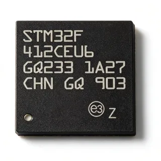
STM32F413CGU6 - 1.5MB Flash ARM Cortex-M4F MCU | STMicroelectronics
MPN: STM32F413CGU6 ✓ 啟用中STM32F413CGU6 概覽
What is a microcontroller? A microcontroller (MCU) is a compact integrated circuit designed to govern a specific operation in an embedded system. It integrates a processor core, memory (Flash and RAM), and programmable input/output peripherals on a single chip. Microcontrollers are the brains of countless electronic devices, from automotive engine control units to IoT sensors and consumer electronics. The STM32F413CGU6 belongs to the STM32F4 family, which is known for its balance of performance, power efficiency, and peripheral integration, making it a popular choice for industrial, consumer, and IoT applications.
Key features of the STM32F413CGU6 include 1.5 MB of Flash memory and 320 KB of SRAM, providing ample storage for complex firmware. It supports a wide supply voltage range of 1.7V to 3.6V, making it suitable for battery-powered devices. The MCU includes a comprehensive set of peripherals: multiple USARTs, SPIs, I2Cs, a USB OTG FS, a CAN controller, a 12-bit ADC with 16 channels, and advanced timers. It also features a true random number generator (RNG), a cryptographic acceleration cell (AES), and a real-time clock (RTC).
Technically, the STM32F413CGU6 leverages the ARM Cortex-M4F core with DSP instructions and a single-precision FPU, enabling efficient execution of signal processing algorithms. The device operates over a temperature range of -40°C to +85°C (industrial grade) and is available in a UFQFPN-48 package with a 7x7 mm footprint. The MCU supports various low-power modes, including Sleep, Stop, and Standby, to optimize energy consumption in battery-operated applications.
Typical applications include industrial control systems, motor drives, IoT gateways, smart home devices, and portable medical equipment. The rich connectivity options and high memory capacity make it ideal for applications requiring complex user interfaces, communication protocols, and data logging.
When designing with this MCU, ensure proper decoupling of the power supply pins with 100nF capacitors placed close to each VDD pin. The VDDA pin should be connected to a clean analog supply, and the VREF+ pin should be decoupled with a 1uF capacitor for accurate ADC conversions. Additionally, the BOOT0 pin configuration must be set correctly for the desired boot mode (Flash, System memory, or SRAM).
直接替換替代品,適用於 STM32F413CGU6 — 相同封裝,腳位對腳位相容。需重新設計 PCB 的不同封裝零件不列入。
此系列的變體
與下列產品可直接替換的同系列型號: STM32F413CGU6 (相同外形與佔位) — 差異在於 Core, Flash Memory, Package, SRAM, Timers.
STM32F413CHU6
✅ 直接替換 ⚠️ 規格未經驗證📋 參考替代品(不在目錄中)
STM32F412CGU6
✅ 直接替換 ⚠️ 規格未經驗證📋 參考替代品(不在目錄中)
STM32F411CEU6
✅ 直接替換 ⚠️ 規格未經驗證聯絡詢價
查看資料表 →LPC4357FET256
⚡ 相同封裝 ⚠️ 規格未經驗證聯絡詢價
查看資料表 →R5F564MLDDFC
⚡ 相同封裝 ⚠️ 規格未經驗證📋 參考替代品(不在目錄中)
STM32F413CGU6 最大額定值與電氣特性
| Core | ARM Cortex-M4F with FPU |
| 最大時脈頻率 | 100 MHz |
| Flash Memory | 1.5 MB |
| SRAM | 320 KB |
| Supply Voltage Range | 1.7 V to 3.6 V |
| 封裝 | UFQFPN-48 (7x7 mm) |
| 工作溫度範圍 | -40C to +85C |
| Number of I/O Pins | 36 |
| ADC Resolution | 12-bit |
| Number of ADC Channels | 16 |
| USART Interfaces | 6 |
| SPI Interfaces | 3 |
| I2C Interfaces | 3 |
| USB OTG FS | 1 |
| CAN Interface | 1 |
| Timers | 11 (including advanced-control) |
| DMA Channels | 16 |
| Cryptographic Acceleration | AES-256 |
| Random Number Generator | Yes |
| RTC | Yes |
| Low-Power Modes | Sleep, Stop, Standby |
| RoHS 狀態 | Compliant |
STM32F413CGU6 腳位配置
| 腳位 1 | VBAT — Battery backup for RTC and backup registers |
| 腳位 2 | PC13 — GPIO, TAMPER-RTC, WKUP2 |
| 腳位 3 | PC14 — GPIO, OSC32_IN |
| 腳位 4 | PC15 — GPIO, OSC32_OUT |
| 腳位 5 | PF0 — GPIO, OSC_IN |
| 腳位 6 | PF1 — GPIO, OSC_OUT |
| 腳位 7 | NRST — Reset (active low) |
| 腳位 8 | PC0 — GPIO, ADC12_IN10 |
| 腳位 9 | PC1 — GPIO, ADC12_IN11 |
| 腳位 10 | PC2 — GPIO, ADC12_IN12 |
| 腳位 11 | PC3 — GPIO, ADC12_IN13 |
| 腳位 12 | VDD — Digital power supply |
| 腳位 13 | VSS — Digital ground |
| 腳位 14 | PC4 — GPIO, ADC12_IN14 |
| 腳位 15 | PC5 — GPIO, ADC12_IN15 |
| 腳位 16 | PB0 — GPIO, ADC12_IN8, TIM3_CH3 |
| 腳位 17 | PB1 — GPIO, ADC12_IN9, TIM3_CH4 |
| 腳位 18 | PB2 — GPIO, BOOT1 |
| 腳位 19 | PB10 — GPIO, I2C2_SCL, USART3_TX |
| 腳位 20 | PB11 — GPIO, I2C2_SDA, USART3_RX |
| 腳位 21 | VSS — Ground |
| 腳位 22 | VDD — Power supply |
| 腳位 23 | PB12 — GPIO, SPI2_NSS, I2C2_SMBA |
| 腳位 24 | PB13 — GPIO, SPI2_SCK |
| 腳位 25 | PB14 — GPIO, SPI2_MISO |
| 腳位 26 | PB15 — GPIO, SPI2_MOSI |
| 腳位 27 | PC6 — GPIO, TIM3_CH1, SDIO_D6 |
| 腳位 28 | PC7 — GPIO, TIM3_CH2, SDIO_D7 |
| 腳位 29 | PC8 — GPIO, TIM3_CH3, SDIO_D0 |
| 腳位 30 | PC9 — GPIO, TIM3_CH4, SDIO_D1 |
| 腳位 31 | PA0 — GPIO, WKUP1, ADC12_IN0, TIM2_CH1 |
| 腳位 32 | PA1 — GPIO, ADC12_IN1, TIM2_CH2 |
| 腳位 33 | PA2 — GPIO, ADC12_IN2, TIM2_CH3, USART2_TX |
| 腳位 34 | PA3 — GPIO, ADC12_IN3, TIM2_CH4, USART2_RX |
| 腳位 35 | VSS — Ground |
| 腳位 36 | VDD — Power supply |
| 腳位 37 | PA4 — GPIO, ADC12_IN4, SPI1_NSS |
| 腳位 38 | PA5 — GPIO, ADC12_IN5, SPI1_SCK, DAC_OUT2 |
| 腳位 39 | PA6 — GPIO, ADC12_IN6, SPI1_MISO, TIM3_CH1 |
| 腳位 40 | PA7 — GPIO, ADC12_IN7, SPI1_MOSI, TIM3_CH2 |
| 腳位 41 | PB6 — GPIO, I2C1_SCL, USART1_TX, TIM4_CH1 |
| 腳位 42 | PB7 — GPIO, I2C1_SDA, USART1_RX, TIM4_CH2 |
| 腳位 43 | BOOT0 — Boot mode selection |
| 腳位 44 | PB8 — GPIO, I2C1_SCL, CAN_RX, TIM4_CH3 |
| 腳位 45 | PB9 — GPIO, I2C1_SDA, CAN_TX, TIM4_CH4 |
| 腳位 46 | VSS — Ground |
| 腳位 47 | VDD — Power supply |
| 腳位 48 | PA8 — GPIO, MCO1, TIM1_CH1, USB_OTG_FS_SOF |
典型應用
STM32F413CGU6 適用於 6 應用s: Industrial Control Systems, IoT Gateways, Motor Drives, Smart Home Devices, Portable Medical Equipment, Audio Processing.
Industrial Control Systems
The STM32F413CGU6 is ideal for industrial control systems due to its 100 MHz Cortex-M4F core, advanced timers, and CAN interface. It can handle real-time control loops, motor control, and PLC applications. The wide temperature range (-40°C to +85°C) ensures reliable operation in harsh factory environments. Its 1.5 MB Flash allows for complex control algorithms and data logging. The MCU's multiple UARTs and SPIs enable communication with sensors, actuators, and HMI panels. The cryptographic acceleration unit provides secure communication for industrial IoT applications.
推薦
IoT Gateways
The STM32F413CGU6 is well-suited for IoT gateways due to its rich connectivity options, including USB OTG FS, CAN, UART, SPI, and I2C. It can aggregate data from multiple sensors and communicate with cloud services via Ethernet or Wi-Fi modules. The 1.5 MB Flash provides ample space for protocol stacks (MQTT, CoAP) and over-the-air updates. The low-power modes (Sleep, Stop, Standby) help reduce energy consumption in battery-powered gateways. The AES-256 encryption ensures secure data transmission, making it a trusted choice for smart home and industrial IoT applications.
推薦
Motor Drives
The STM32F413CGU6 is an excellent choice for motor drives, including BLDC, PMSM, and stepper motors. Its advanced-control timers (TIM1 and TIM8) generate high-resolution PWM signals with dead-time insertion, essential for driving power stages. The 100 MHz Cortex-M4F core with FPU can execute Field-Oriented Control (FOC) algorithms in real-time. The 12-bit ADC with 16 channels allows precise current and voltage sensing. The CAN interface enables communication with higher-level controllers in industrial automation. The MCU's robust design and wide temperature range make it suitable for demanding motor control environments.
推薦
Smart Home Devices
The STM32F413CGU6 is perfect for smart home devices such as smart thermostats, lighting controllers, and security systems. Its low-power modes enable battery-powered operation, while the rich peripheral set supports various sensors (temperature, humidity, motion) and actuators (relays, LEDs). The USB OTG FS allows direct connection to smartphones for configuration and firmware updates. The AES-256 encryption secures communication with smart home hubs. The compact UFQFPN-48 package fits into small form-factor designs, making it ideal for wall-mounted and embedded applications.
推薦
Portable Medical Equipment
The STM32F413CGU6 is suitable for portable medical devices like glucose monitors, pulse oximeters, and portable ECG monitors. Its low-power modes extend battery life, crucial for wearable devices. The 12-bit ADC with 16 channels accurately captures biosignals. The cryptographic acceleration unit ensures secure storage and transmission of patient data, complying with healthcare regulations. The 1.5 MB Flash allows for complex signal processing algorithms and data logging. The wide supply voltage range (1.7V to 3.6V) supports operation from a single lithium-ion cell.
推薦
Audio Processing
The STM32F413CGU6 can be used for audio processing applications such as voice recognition, audio effects, and portable audio players. The Cortex-M4F core with FPU and DSP instructions efficiently executes audio algorithms like filtering and FFT. The I2S interface (via SPI) connects to audio codecs and DACs. The 1.5 MB Flash can store audio samples and firmware. The USB OTG FS enables audio streaming to and from a host. The MCU's low-power modes are beneficial for battery-powered audio devices.
推薦
推薦產品摘要
工程參考資料,適用於 STM32F413CGU6 — 比較、設計指引及合規資訊。
選型指南
與替代品比較
| 參數 | 本產品 | STM32F413CHU6 | STM32F412CGU6 | STM32F411CEU6 | LPC4357FET256 | R5F564MLDDFC |
|---|---|---|---|---|---|---|
| Package | UFQFPN-48 | UFQFPN-48 | UFQFPN-48 | UFQFPN-48 | UFQFPN-48 | UFQFPN-48 |
| Brand | STMicroelectronics | STMicroelectronics | STMicroelectronics | STMicroelectronics | NXP Semiconductors | Renesas Electronics |
| Core | ARM Cortex-M4F | ARM Cortex-M4F | ARM Cortex-M4F | ARM Cortex-M4F | ARM Cortex-M4F + M0 | RXv3 |
| Maximum Clock Frequency | 100 MHz | 100 MHz | 100 MHz | 100 MHz | 204 MHz | 120 MHz |
| Flash Memory | 1.5 MB | 1.5 MB | 1 MB | 512 KB | 1 MB | 2 MB |
| SRAM | 320 KB | 320 KB | 256 KB | 128 KB | 136 KB | 640 KB |
| Supply Voltage Range | 1.7V to 3.6V | 1.7V to 3.6V | 1.7V to 3.6V | 1.7V to 3.6V | 2.2V to 3.6V | 2.7V to 3.6V |
| Number of I/O Pins | 36 | 36 | 36 | 36 | 36 | 36 |
| ADC Resolution | 12-bit | 12-bit | 12-bit | 12-bit | 12-bit | 12-bit |
| USB OTG FS | Yes | Yes | Yes | Yes | Yes | Yes |
| CAN Interface | Yes | Yes | Yes | No | Yes | Yes |
| Cryptographic Acceleration | AES-256 | AES-256 | AES-256 | No | AES-256 | AES-128/256 |
主要差異化特點
- Larger Flash and SRAM compared to STM32F411CEU6 (對比STM32F411CEU6)
- Integrated cryptographic acceleration (AES-256) (對比STM32F411CEU6)
- CAN interface for industrial networking (對比STM32F411CEU6)
設計說明
Decouple each VDD pin with a 100nF ceramic capacitor placed as close to the pin as possible. Additionally, connect a 4.7uF capacitor to the main power rail. The VDDA pin should be connected to a clean analog supply, and VREF+ should be decoupled with a 1uF capacitor for accurate ADC conversions. For battery-powered designs, use the VBAT pin to back up the RTC and backup registers with a coin cell.
For the UFQFPN-48 package, ensure the exposed pad (EP) is soldered to the PCB ground plane for thermal and electrical performance. Use a 7x7 mm footprint with proper solder mask openings. Route high-speed signals (e.g., SPI, USB) with controlled impedance and keep traces short. Place the crystal oscillator (HSE) close to the OSC_IN/OSC_OUT pins with load capacitors as specified in the datasheet.
Ensure the BOOT0 pin is configured correctly for the desired boot mode. For normal operation from Flash, BOOT0 should be tied low through a resistor. Do not leave the NRST pin floating; connect a 100nF capacitor to ground for noise immunity. When using the ADC, avoid digital switching noise on the VDDA pin by adding an LC filter. Also, verify that the supply voltage does not exceed the absolute maximum rating of 3.6V.
合規資訊
RoHS compliant per STMicroelectronics product page. Not AEC-Q100 qualified (industrial grade only).