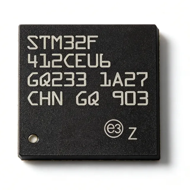
STM32F412CEU6 - 100MHz ARM Cortex-M4F MCU, 512KB Flash | STMicroelectronics
MPN: STM32F412CEU6 ✓ 啟用中STM32F412CEU6 概覽
A microcontroller (MCU) is a compact integrated circuit designed to govern a specific operation in an embedded system. It contains a processor core, memory, and programmable input/output peripherals on a single chip. The STM32F412CEU6 belongs to the STM32F4 series, which is part of the broader STM32 family of 32-bit flash microcontrollers based on the ARM Cortex-M processor. This hierarchy places it within the embedded processing domain, where it serves as the central control unit for a wide range of electronic devices.
Key features include a 100 MHz ARM Cortex-M4F core with DSP instructions and a floating-point unit (FPU), enabling efficient signal processing and mathematical computations. The device offers a rich set of peripherals: multiple USARTs, SPIs, I2Cs, a full-speed USB 2.0 OTG, a 12-bit ADC with up to 16 channels, a 12-bit DAC, advanced timers, and a true random number generator (RNG). It also supports external memory interfaces via FSMC, allowing expansion of memory beyond the internal flash and SRAM.
Technically, the STM32F412CEU6 is fabricated using a 90nm process technology, providing a balance between performance and power consumption. It operates from a 1.7V to 3.6V supply, with multiple low-power modes (Sleep, Stop, Standby) to optimize energy efficiency. The device includes a nested vectored interrupt controller (NVIC) for efficient interrupt handling, and a memory protection unit (MPU) for enhanced application security.
Typical applications include industrial control systems, motor drives, consumer electronics, IoT gateways, and audio processing. Its combination of processing power, connectivity, and low-power modes makes it ideal for battery-powered devices and real-time control applications. For instance, in an IoT gateway, the STM32F412CEU6 can manage sensor data acquisition, run communication protocols, and interface with cloud services via its USB and UART interfaces.
When designing with this MCU, ensure proper decoupling of the power supply pins with 100nF capacitors placed close to each VDD pin, and a 4.7uF bulk capacitor. The VDDA pin should be connected to a clean analog supply, and the VREF+ pin to a stable reference voltage for accurate ADC conversions. Also, configure the boot pins correctly to select the desired boot mode (flash, system memory, or SRAM) during development.
直接替換替代品,適用於 STM32F412CEU6 — 相同封裝,腳位對腳位相容。需重新設計 PCB 的不同封裝零件不列入。
此系列的變體
與下列產品可直接替換的同系列型號: STM32F412CEU6 (相同外形與佔位) — 差異在於 Core, Package, Timers, Operating Temperature, ADC.
STM32F411CEU6
聯絡詢價
查看資料表 →STM32F405RGT6
聯絡詢價
查看資料表 →STM32F412CEU6TR
📋 參考替代品(不在目錄中)
STM32F412RGU6
📋 參考替代品(不在目錄中)
LPC4337FBD144
📋 參考替代品(不在目錄中)
STM32F412CEU6 最大額定值與電氣特性
| Core | ARM Cortex-M4F |
| Max Clock Speed | 100 MHz |
| Flash Memory | 512 KB |
| SRAM | 128 KB |
| 供應電壓 | 1.7 V to 3.6 V |
| 封裝 | UFQFPN-48 (7x7 mm) |
| GPIO Pins | 36 |
| ADC Resolution | 12-bit |
| ADC Channels | 16 |
| DAC Resolution | 12-bit |
| DAC Channels | 2 |
| USART | 4 |
| SPI | 3 |
| I2C | 3 |
| USB | USB 2.0 OTG FS |
| Timers | 8 (including advanced timers) |
| 工作溫度 | -40C to +85C |
| RoHS 狀態 | Compliant |
STM32F412CEU6 腳位配置
| 腳位 1 | VDD — Power supply |
| 腳位 2 | PA0 — GPIO / ADC input |
| 腳位 3 | PA1 — GPIO / ADC input |
| 腳位 4 | PA2 — GPIO / USART2_TX |
| 腳位 5 | PA3 — GPIO / USART2_RX |
| 腳位 6 | VSS — Ground |
| 腳位 7 | PA4 — GPIO / DAC_OUT1 |
| 腳位 8 | PA5 — GPIO / DAC_OUT2 |
| 腳位 9 | PA6 — GPIO / SPI1_MISO |
| 腳位 10 | PA7 — GPIO / SPI1_MOSI |
| 腳位 11 | PB0 — GPIO / ADC input |
| 腳位 12 | PB1 — GPIO / ADC input |
| 腳位 13 | PB2 — GPIO / BOOT1 |
| 腳位 14 | PB10 — GPIO / I2C2_SCL |
| 腳位 15 | PB11 — GPIO / I2C2_SDA |
| 腳位 16 | VDD — Power supply |
| 腳位 17 | PB12 — GPIO / SPI2_NSS |
| 腳位 18 | PB13 — GPIO / SPI2_SCK |
| 腳位 19 | PB14 — GPIO / SPI2_MISO |
| 腳位 20 | PB15 — GPIO / SPI2_MOSI |
| 腳位 21 | PC13 — GPIO / RTC output |
| 腳位 22 | PC14 — GPIO / OSC32_IN |
| 腳位 23 | PC15 — GPIO / OSC32_OUT |
| 腳位 24 | VSS — Ground |
| 腳位 25 | PH0 — OSC_IN |
| 腳位 26 | PH1 — OSC_OUT |
| 腳位 27 | NRST — Reset |
| 腳位 28 | PC0 — GPIO / ADC input |
| 腳位 29 | PC1 — GPIO / ADC input |
| 腳位 30 | PC2 — GPIO / ADC input |
| 腳位 31 | PC3 — GPIO / ADC input |
| 腳位 32 | VDD — Power supply |
| 腳位 33 | PC4 — GPIO / ADC input |
| 腳位 34 | PC5 — GPIO / ADC input |
| 腳位 35 | PB3 — GPIO / SPI1_SCK |
| 腳位 36 | PB4 — GPIO / SPI1_NSS |
| 腳位 37 | PB5 — GPIO / I2C1_SMBA |
| 腳位 38 | PB6 — GPIO / I2C1_SCL |
| 腳位 39 | PB7 — GPIO / I2C1_SDA |
| 腳位 40 | BOOT0 — Boot mode selection |
| 腳位 41 | PB8 — GPIO / CAN_RX |
| 腳位 42 | PB9 — GPIO / CAN_TX |
| 腳位 43 | VSS — Ground |
| 腳位 44 | PA8 — GPIO / MCO1 |
| 腳位 45 | PA9 — GPIO / USART1_TX |
| 腳位 46 | PA10 — GPIO / USART1_RX |
| 腳位 47 | PA11 — GPIO / USB_DM |
| 腳位 48 | PA12 — GPIO / USB_DP |
典型應用
STM32F412CEU6 適用於 6 應用s: Industrial Control, IoT Gateway, Consumer Electronics, Motor Drive, Audio Processing, Test and Measurement.
Industrial Control
The STM32F412CEU6 is ideal for industrial control systems due to its 100 MHz Cortex-M4F core, advanced timers, and 12-bit ADC. It can handle real-time control loops, motor control, and PLC applications. The device's multiple USARTs and SPIs enable communication with sensors, actuators, and industrial networks. Its wide operating voltage range and low-power modes ensure reliable operation in harsh environments. For example, in a motor control application, the advanced timers generate PWM signals with dead-time insertion, while the ADC reads current feedback for closed-loop control. The FPU accelerates complex control algorithms, and the MPU provides memory protection for safety-critical tasks.
推薦
IoT Gateway
The STM32F412CEU6 is well-suited for IoT gateways, providing a balance of processing power, connectivity, and low power consumption. Its USB 2.0 OTG FS interface allows direct connection to peripherals or host devices, while multiple UARTs and SPIs interface with sensors and wireless modules. The device can run communication protocols like MQTT and CoAP, and its low-power modes enable battery-powered operation. In a typical IoT gateway, the MCU collects data from sensors via I2C or SPI, processes it locally, and transmits it to the cloud via a Wi-Fi or cellular module connected through UART. The RNG enhances security for encryption protocols.
推薦
Consumer Electronics
The STM32F412CEU6 is used in consumer electronics such as smart home devices, wearables, and audio equipment. Its compact UFQFPN-48 package and low-power modes make it ideal for portable devices. The 12-bit DAC and audio interfaces support audio playback, while the USB interface enables charging and data transfer. For example, in a smart speaker, the MCU handles audio decoding, voice recognition, and network connectivity. The FPU accelerates audio processing algorithms, and the multiple timers generate precise timing for user interface controls.
推薦
Motor Drive
The STM32F412CEU6 excels in motor drive applications, offering advanced timers with dead-time generation, a 12-bit ADC for current sensing, and a 100 MHz core for real-time control. It supports various motor types, including BLDC, PMSM, and stepper motors. In a BLDC motor drive, the MCU generates six-step PWM signals, reads Hall sensor or encoder feedback, and implements field-oriented control (FOC) algorithms. The FPU accelerates the mathematical computations required for FOC, and the ADC samples phase currents with high resolution. The device's robust peripheral set and industrial temperature range make it suitable for factory automation and robotics.
推薦
Audio Processing
The STM32F412CEU6 is capable of audio processing tasks such as audio playback, voice recognition, and sound effects generation. Its 100 MHz Cortex-M4F with FPU can handle real-time audio algorithms, and the 12-bit DAC provides analog audio output. The device supports I2S interfaces for connecting external audio codecs. In a voice-controlled device, the MCU captures audio via a microphone, processes it with DSP algorithms, and triggers actions. The low-power modes allow for always-on listening in battery-powered devices.
推薦
Test and Measurement
The STM32F412CEU6 is used in test and measurement equipment such as data loggers, oscilloscopes, and signal generators. Its high-speed ADC and DAC, along with multiple timers, enable precise signal acquisition and generation. The USB interface allows connection to a PC for data analysis. In a data logger, the MCU samples analog signals at high rates, stores data in flash or external memory via FSMC, and communicates with a host via USB. The FPU processes the data for filtering and analysis.
推薦
推薦產品摘要
工程參考資料,適用於 STM32F412CEU6 — 比較、設計指引及合規資訊。
選型指南
與替代品比較
| 參數 | 本產品 | STM32F411CEU6 | STM32F412CEU6TR | STM32F412RGU6 | STM32F405RGT6 | LPC4337FBD144 |
|---|---|---|---|---|---|---|
| Package | UFQFPN-48 (7x7 mm) | UFQFPN-48 (7x7 mm) - same | UFQFPN-48 (7x7 mm) - same | UFQFPN-64 (9x9 mm) - different | LQFP-64 (10x10 mm) - different | LQFP-144 (20x20 mm) - different |
| Brand | STMicroelectronics | STMicroelectronics | STMicroelectronics | STMicroelectronics | STMicroelectronics | NXP Semiconductors |
| Core | ARM Cortex-M4F | ARM Cortex-M4F | ARM Cortex-M4F | ARM Cortex-M4F | ARM Cortex-M4F | ARM Cortex-M4F + M0 |
| Max Clock Speed | 100 MHz | 100 MHz | 100 MHz | 100 MHz | 168 MHz | 204 MHz |
| Flash Memory | 512 KB | 512 KB | 512 KB | 512 KB | 1 MB | 1 MB |
| SRAM | 128 KB | 128 KB | 128 KB | 128 KB | 192 KB | 136 KB |
| USB | USB 2.0 OTG FS | None | USB 2.0 OTG FS | USB 2.0 OTG FS | USB 2.0 OTG FS | USB 2.0 OTG HS |
| ADC Channels | 16 | 16 | 16 | 16 | 16 | 8 |
主要差異化特點
- Integrated USB 2.0 OTG FS (對比STM32F411CEU6)
- True Random Number Generator (RNG) (對比STM32F411CEU6)
- Compact UFQFPN-48 package (對比STM32F412RGU6)
設計說明
Decouple each VDD pin with a 100nF ceramic capacitor placed as close as possible to the pin, and add a 4.7uF bulk capacitor. Connect VDDA to a clean analog supply through a ferrite bead, and VREF+ to a stable reference voltage (e.g., 3.3V) for accurate ADC conversions. Ensure VDD and VDDA are within the 1.7V-3.6V range.
For the UFQFPN-48 package, ensure the exposed pad (EP) is soldered to a ground plane for thermal and electrical performance. Provide adequate thermal vias under the pad to dissipate heat. Keep high-speed signals (USB, SPI) short and impedance-controlled. Place the crystal oscillator close to PH0/PH1 with load capacitors as specified in the datasheet.
Configure the BOOT0 and BOOT1 pins correctly to select the desired boot mode (flash, system memory, or SRAM). Do not leave unused GPIO pins floating; configure them as outputs or enable internal pull-ups/pull-downs. Ensure the NRST pin is pulled high with a 100nF capacitor to ground for reliable reset. When using the USB interface, add the required 1.5k pull-up on USB_DP and proper ESD protection.
合規資訊
RoHS compliant per STMicroelectronics product page. Not AEC-Q100 qualified; for automotive, consider STM32F412CEU6Q (if available).


