STM8S105C6T6 - 8-bit MCU, 16MHz, 32KB Flash | STMicroelectronics
MPN: STM8S105C6T6 ✓ 啟用中STM8S105C6T6 概覽
An 8-bit microcontroller (MCU) is a single-chip computer with an 8-bit data bus, integrating a processor core, memory, and programmable input/output peripherals. The STM8S105C6T6 belongs to the STM8S family, which is part of the broader STM8 microcontroller series, positioned below the 32-bit STM32 family in STMicroelectronics' product hierarchy. It is designed for applications requiring moderate processing power, low power consumption, and rich peripheral integration, such as industrial control, home appliances, and automotive body electronics.
Key features include a 10-bit analog-to-digital converter (ADC) with up to 10 channels, multiple 16-bit timers, and a full set of communication interfaces: UART, SPI, and I2C. The device also integrates a true data EEPROM with up to 300,000 write/erase cycles, enabling data storage without external memory. The STM8 core operates at up to 16 MHz, delivering 16 MIPS throughput, and supports a wide range of clock sources including internal RC oscillators and external crystals.
The STM8S105C6T6 is built on a high-density Flash technology, providing robust program memory endurance and fast programming. The architecture includes a nested interrupt controller with 28 interrupt vectors, enhancing real-time responsiveness. The device also features a low-power mode with typical current consumption of 5 µA in Halt mode, making it suitable for battery-powered applications.
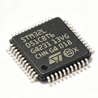
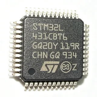
Typical applications include industrial automation, home appliances (e.g., washing machines, air conditioners), power tools, and automotive body control modules. The rich peripheral set and 5V-tolerant I/Os allow direct interfacing with sensors, relays, and displays without level shifting. The LQFP-48 package provides 38 I/O pins, offering ample connectivity for control and communication.
When designing with this MCU, ensure proper decoupling of the VDD and VDDA pins with 100 nF capacitors placed close to the device. The NRST pin should be connected to a 100 nF capacitor to ground for reliable reset. For applications requiring precise timing, use an external crystal oscillator with load capacitors as specified in the datasheet.
直接替換替代品,適用於 STM8S105C6T6 — 相同封裝,腳位對腳位相容。需重新設計 PCB 的不同封裝零件不列入。
此系列的變體
與下列產品可直接替換的同系列型號: STM8S105C6T6 (相同外形與佔位) — 差異在於 Package, ADC Resolution, Core, Flash Program Memory, Operating Temperature Range.
STM8S105C6T6TR
✅ 直接替換📋 參考替代品(不在目錄中)
STM8S105C8T6
✅ 直接替換📋 參考替代品(不在目錄中)
STM8AF6268TCX
✅ 直接替換📋 參考替代品(不在目錄中)
STM8S105C4T6
✅ 直接替換 ⚠️ 規格未經驗證聯絡詢價
查看資料表 →STM8S105C6T6 最大額定值與電氣特性
| Core | STM8 8-bit CISC |
| 最大時脈頻率 | 16 MHz |
| Program Memory Size | 32 KB (32K x 8) Flash |
| RAM Size | 2 KB |
| Data EEPROM Size | 1 KB |
| Number of I/O Pins | 38 |
| Supply Voltage Range | 2.95 V to 5.5 V |
| ADC Resolution | 10-bit |
| Number of ADC Channels | 10 |
| Timer Count | 3 (16-bit) |
| Communication Interfaces | UART, SPI, I2C |
| 封裝 | LQFP-48 (7x7 mm) |
| 安裝類型 | Surface Mount |
| 工作溫度範圍 | -40°C to +85°C |
| RoHS 狀態 | Compliant |
STM8S105C6T6 腳位配置
| 腳位 1 | PD0 — Port D0, general purpose I/O |
| 腳位 2 | PD1 — Port D1, general purpose I/O |
| 腳位 3 | PD2 — Port D2, general purpose I/O |
| 腳位 4 | PD3 — Port D3, general purpose I/O |
| 腳位 5 | PD4 — Port D4, general purpose I/O |
| 腳位 6 | PD5 — Port D5, general purpose I/O |
| 腳位 7 | PD6 — Port D6, general purpose I/O |
| 腳位 8 | PD7 — Port D7, general purpose I/O |
| 腳位 9 | VSS — Ground |
| 腳位 10 | VDD — Power supply |
| 腳位 11 | PA0 — Port A0, general purpose I/O |
| 腳位 12 | PA1 — Port A1, general purpose I/O |
| 腳位 13 | PA2 — Port A2, general purpose I/O |
| 腳位 14 | PA3 — Port A3, general purpose I/O |
| 腳位 15 | PA4 — Port A4, general purpose I/O |
| 腳位 16 | PA5 — Port A5, general purpose I/O |
| 腳位 17 | PA6 — Port A6, general purpose I/O |
| 腳位 18 | PA7 — Port A7, general purpose I/O |
| 腳位 19 | PB0 — Port B0, general purpose I/O |
| 腳位 20 | PB1 — Port B1, general purpose I/O |
| 腳位 21 | PB2 — Port B2, general purpose I/O |
| 腳位 22 | PB3 — Port B3, general purpose I/O |
| 腳位 23 | PB4 — Port B4, general purpose I/O |
| 腳位 24 | PB5 — Port B5, general purpose I/O |
| 腳位 25 | PB6 — Port B6, general purpose I/O |
| 腳位 26 | PB7 — Port B7, general purpose I/O |
| 腳位 27 | PC0 — Port C0, general purpose I/O |
| 腳位 28 | PC1 — Port C1, general purpose I/O |
| 腳位 29 | PC2 — Port C2, general purpose I/O |
| 腳位 30 | PC3 — Port C3, general purpose I/O |
| 腳位 31 | PC4 — Port C4, general purpose I/O |
| 腳位 32 | PC5 — Port C5, general purpose I/O |
| 腳位 33 | PC6 — Port C6, general purpose I/O |
| 腳位 34 | PC7 — Port C7, general purpose I/O |
| 腳位 35 | NRST — Reset (active low) |
| 腳位 36 | VSS — Ground |
| 腳位 37 | VDD — Power supply |
| 腳位 38 | OSCIN — Oscillator input |
| 腳位 39 | OSCOUT — Oscillator output |
| 腳位 40 | PE0 — Port E0, general purpose I/O |
| 腳位 41 | PE1 — Port E1, general purpose I/O |
| 腳位 42 | PE2 — Port E2, general purpose I/O |
| 腳位 43 | PE3 — Port E3, general purpose I/O |
| 腳位 44 | PE4 — Port E4, general purpose I/O |
| 腳位 45 | PE5 — Port E5, general purpose I/O |
| 腳位 46 | PE6 — Port E6, general purpose I/O |
| 腳位 47 | PE7 — Port E7, general purpose I/O |
| 腳位 48 | VDDA — Analog power supply |
典型應用
STM8S105C6T6 適用於 6 應用s: Industrial Automation, Home Appliances, Automotive Body Electronics, Power Tools, Smart Sensors, Consumer Electronics.
Industrial Automation
The STM8S105C6T6 is ideal for industrial automation due to its robust 5V operation, rich peripheral set (UART, SPI, I2C, timers, ADC), and wide temperature range. It can interface directly with sensors, actuators, and relays without level shifting, simplifying design. The 32 KB Flash and 2 KB RAM are sufficient for control algorithms, while the true EEPROM stores calibration data and fault logs. The 16 MHz core provides fast response for real-time control loops, and the low-power Halt mode reduces energy consumption in standby. Compared to 32-bit MCUs, it offers lower cost and adequate performance for tasks like motor control, conveyor monitoring, and process control.
推薦
Home Appliances
In home appliances such as washing machines, air conditioners, and microwave ovens, the STM8S105C6T6 provides a cost-effective control solution. Its 5V operation directly interfaces with relays, buzzers, and LED displays, while the 10-bit ADC reads temperature sensors and potentiometers. The multiple timers generate PWM signals for motor speed control and heater regulation. The integrated EEPROM stores user settings and error codes, eliminating external memory. The device's robustness against electrical noise and wide voltage range ensures reliable operation in household environments. Its low power consumption in Halt mode is beneficial for standby power reduction, meeting energy efficiency standards.
推薦
Automotive Body Electronics
The STM8S105C6T6 is suitable for automotive body electronics like window lifters, mirror controls, and lighting modules. Although not AEC-Q100 qualified, it can be used in non-safety-critical applications with proper derating. The 5V supply and 5V-tolerant I/Os interface with automotive sensors and switches. The UART and LIN (via software) enable communication with body control modules. The 16 MHz core handles real-time tasks like PWM dimming and switch debouncing. The wide temperature range (-40°C to +85°C) covers most automotive environments. For higher reliability, the STM8AF6268TCX is recommended as a drop-in alternative.
推薦
Power Tools
The STM8S105C6T6 is well-suited for power tools like drills, saws, and grinders, where it manages motor control, battery monitoring, and safety features. The 10-bit ADC monitors battery voltage and current, while the timers generate PWM for variable speed control. The 5V operation is compatible with battery packs (e.g., 12V, 18V) with a simple regulator. The robust I/Os handle high-current switching via external MOSFET drivers. The integrated EEPROM stores usage logs and calibration data. The compact LQFP-48 package fits in handheld tool PCBs, and the low-power modes extend battery life during idle periods.
推薦
Smart Sensors
The STM8S105C6T6 can be used in smart sensors for environmental monitoring, building automation, and IoT edge nodes. Its UART, SPI, and I2C interfaces connect to various sensors (temperature, humidity, gas) and wireless modules (e.g., LoRa, Zigbee). The 10-bit ADC reads analog sensor outputs, and the timers handle periodic sampling. The 32 KB Flash stores firmware for signal processing and calibration algorithms. The low-power Halt mode (5 µA) is ideal for battery-powered sensors, enabling long deployment life. The 5V operation simplifies interfacing with industrial sensors that require higher voltage levels.
推薦
Consumer Electronics
In consumer electronics like remote controls, toys, and small appliances, the STM8S105C6T6 offers a low-cost, feature-rich MCU. Its 5V operation and 38 I/Os allow direct connection to buttons, LEDs, and small displays. The UART and I2C interfaces enable communication with other ICs like audio codecs and EEPROMs. The 16 MHz core provides enough processing power for user interface logic and simple algorithms. The integrated EEPROM stores user preferences and device settings. The compact LQFP-48 package is suitable for space-constrained designs, and the wide supply range accommodates battery-powered devices.
推薦
推薦產品摘要
工程參考資料,適用於 STM8S105C6T6 — 比較、設計指引及合規資訊。
選型指南
與替代品比較
| 參數 | 本產品 | STM8S105C6T6TR | STM8S105C8T6 | STM8AF6268TCX | STM8S105C4T6 |
|---|---|---|---|---|---|
| Package | LQFP-48 | LQFP-48 | LQFP-48 | LQFP-48 | LQFP-48 |
| Brand | STMicroelectronics | STMicroelectronics | STMicroelectronics | STMicroelectronics | STMicroelectronics |
| Flash Memory | 32 KB | 32 KB | 64 KB | 32 KB | 16 KB |
| RAM | 2 KB | 2 KB | 6 KB | 2 KB | 1 KB |
| EEPROM | 1 KB | 1 KB | 2 KB | 1 KB | 640 B |
| Automotive Grade | No | No | No | Yes (AEC-Q100) | No |
| Max Clock | 16 MHz | 16 MHz | 16 MHz | 16 MHz | 16 MHz |
| I/O Pins | 38 | 38 | 38 | 38 | 38 |
主要差異化特點
- True data EEPROM with 300k write/erase cycles (對比STM8S105C8T6)
- 5V operation with 5V-tolerant I/Os (對比N76E003AT20)
- Wide operating temperature range (對比STM8S105C4T6)
設計說明
Decouple the VDD and VDDA pins with 100 nF ceramic capacitors placed as close to the pins as possible. Additionally, use a 4.7 µF bulk capacitor on the main supply rail. The VDDA pin should be connected to VDD through a ferrite bead or a low-pass filter to reduce noise on the analog supply, which is critical for ADC accuracy.
For the LQFP-48 package, ensure proper solder paste stencil design to avoid bridging between pins. The exposed pad (if present) should be connected to ground with multiple vias for thermal relief. Keep high-speed communication lines (SPI, I2C) short and away from high-current traces to minimize crosstalk.
The NRST pin must be connected to a 100 nF capacitor to ground to ensure reliable reset. Do not leave the NRST pin floating. Also, ensure that the supply voltage does not exceed 5.5V, as this can damage the device. For programming, use the SWIM interface with a 1 kΩ resistor in series to the SWIM pin.
合規資訊
RoHS compliant per STMicroelectronics product page. Not AEC-Q100 qualified; use STM8AF6268TCX for automotive.