STM32F103CBT6 - 72MHz Cortex-M3 128KB Flash MCU | STMicroelectronics
MPN: STM32F103CBT6 ✓ 啟用中| 數量 | 單價 | 小計 |
|---|---|---|
| 1 | $5.62 | $5.62 |
| 10 | $5.05 | $50.50 |
| 100 | $4.4 | $440.00 |
| 500 | $3.78 | $1,890.00 |
| 1,000 | $3.2 | $3,200.00 |
STM32F103CBT6 概覽
What is a microcontroller? An MCU integrates a processor core, on-chip non-volatile memory (Flash), volatile working memory (SRAM), and a set of programmable peripherals onto a single silicon die. Within the embedded-computing hierarchy it sits above a bare microprocessor and below a full system-on-chip, and within ST's own portfolio the STM32F1 mainstream series places the STM32F103CBT6 between the ultra-low-power STM32L family and the higher-performance Cortex-M4 STM32F4 family. The part belongs to the medium-density STM32F103xx performance line, which targets cost-sensitive industrial and consumer control.
Key features include a 72 MHz Cortex-M3 core with single-cycle hardware multiply and divide, a 2.0 V to 3.6 V supply range, an embedded nested vectored interrupt controller with 43 maskable channels, and up to 37 GPIO pins tolerant to 5 V. On-board communication is broad for the class: three USARTs, two I2C buses, two SPI interfaces, one full-speed USB 2.0 device port, and one CAN 2.0B active controller. Two 12-bit ADCs (1 us conversion), one 12-bit DAC, three general-purpose 16-bit timers, one PWM timer, and one basic timer give ample motor-control flexibility.
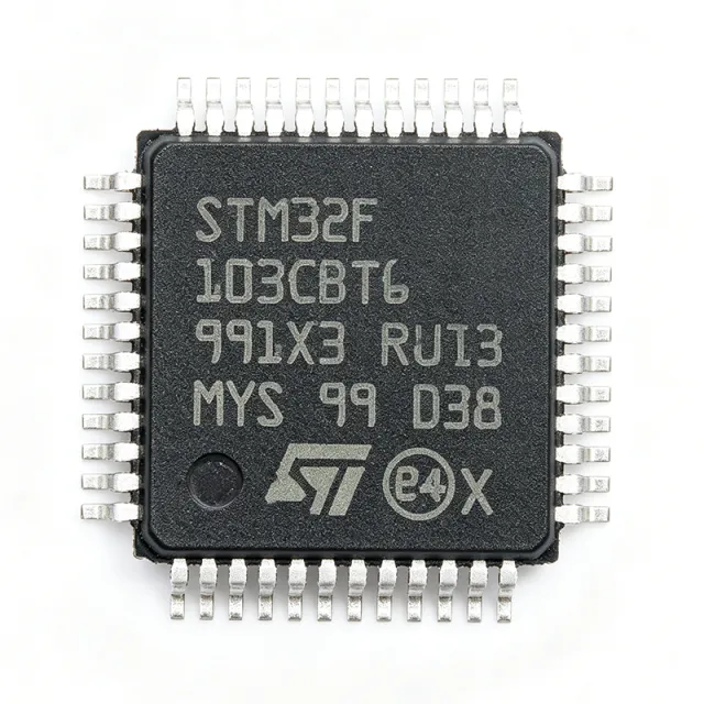
Technically, the clock tree uses an internal 8 MHz RC oscillator plus a 4-16 MHz external crystal and a dedicated 32 kHz RTC oscillator; PLL multiplication reaches 72 MHz. Programming is via SWD or JTAG, with a built-in bootloader selectable via BOOT0/BOOT1. The 7x7 mm LQFP-48 package gives a low-cost, easy-to-assemble footprint suitable for both hand-soldered prototypes and high-volume SMT lines.
Typical applications include industrial control nodes, motor drives, USB-to-CAN fieldbus bridges, medical instruments, smart-home hubs, and IoT gateways, where the combination of USB, CAN, and multiple UARTs positions the part as a communication-rich embedded hub. For design, decouple every VDD pin with 100 nF ceramics plus a single 4.7 uF bulk, place the HSE crystal traces short and guarded, and tie BOOT0 to GND for normal Flash boot or to VDD for system-memory bootloader. This page synthesises distributor pricing, drop-in alternatives (GD32F103CBT6, APM32F103CBT6, AT32F403ACBT7), and practical design notes not found in the ST datasheet.
直接替換替代品,適用於 STM32F103CBT6 — 相同封裝,腳位對腳位相容。需重新設計 PCB 的不同封裝零件不列入。
此系列的變體
與下列產品可直接替換的同系列型號: STM32F103CBT6 (相同外形與佔位) — 差異在於 Package, ADC, Timers, Communication Interfaces, Flash Memory.
快速比較工具 — 選擇替代零件進行並排比較:
STM32F103C8T6
✅ 直接替換✗ 缺貨
$1.02 / 單位
查看資料表 →STM32F103RBT6
✅ 直接替換聯絡詢價
查看資料表 →STM32F103VBT6
✅ 直接替換聯絡詢價
查看資料表 →GD32F103CBT6
✅ 直接替換📋 參考替代品(不在目錄中)
APM32F103CBT6
✅ 直接替換📋 參考替代品(不在目錄中)
CKS32F103CBT6
✅ 直接替換📋 參考替代品(不在目錄中)
AT32F403ACBT7
✅ 直接替換📋 參考替代品(不在目錄中)
STM32F103CBT6 最大額定值與電氣特性
| Core | ARM Cortex-M3 32-bit RISC |
| 最大時脈頻率 | 72 MHz |
| Flash Memory | 128 KB |
| SRAM | 20 KB |
| 供應電壓 | 2.0 V to 3.6 V |
| GPIO Count | 37 (5 V tolerant) |
| ADC | 2x 12-bit, up to 10 channels |
| DAC | 1x 12-bit |
| Timers | 3x 16-bit GP + 1x PWM + 1x basic |
| USART | 3 |
| I2C | 2 |
| SPI | 2 |
| USB | USB 2.0 Full-Speed Device |
| CAN | 1x CAN 2.0B Active |
| 封裝 | LQFP-48 (7x7 mm) |
| 工作溫度 | -40 C to +85 C |
| 安裝類型 | Surface Mount |
| RoHS 狀態 | Compliant |
STM32F103CBT6 腳位配置
| 腳位 1 | VBAT — RTC backup supply |
| 腳位 2 | PC13 — GPIO/Tamper-RTC (5V tolerant) |
| 腳位 3 | PC14 — GPIO/OSC32_IN (5V tolerant) |
| 腳位 4 | PC15 — GPIO/OSC32_OUT (5V tolerant) |
| 腳位 5 | OSC_IN — HSE crystal input |
| 腳位 6 | OSC_OUT — HSE crystal output |
| 腳位 7 | NRST — Reset (active low) |
| 腳位 8 | VSSA — Analog ground |
| 腳位 9 | VDDA — Analog supply (2.0-3.6 V) |
| 腳位 10 | PA0 — GPIO/ADC0/WKUP |
| 腳位 11 | PA1 — GPIO/ADC1 |
| 腳位 12 | PA2 — GPIO/USART2_TX/ADC2 |
| 腳位 13 | PA3 — GPIO/USART2_RX/ADC3 |
| 腳位 14 | PA4 — GPIO/SPI1_NSS/ADC4 |
| 腳位 15 | PA5 — GPIO/SPI1_SCK/ADC5 |
| 腳位 16 | PA6 — GPIO/SPI1_MISO/ADC6 |
| 腳位 17 | PA7 — GPIO/SPI1_MOSI/ADC7 |
| 腳位 18 | PB0 — GPIO/ADC8 |
| 腳位 19 | PB1 — GPIO/ADC9 |
| 腳位 20 | PB2 — GPIO/BOOT1 |
| 腳位 21 | PB10 — GPIO/I2C2_SCL/USART3_TX |
| 腳位 22 | PB11 — GPIO/I2C2_SDA/USART3_RX |
| 腳位 23 | VSS_1 — Digital ground |
| 腳位 24 | VDD_1 — Digital supply (2.0-3.6 V) |
| 腳位 25 | PB12 — GPIO/SPI2_NSS |
| 腳位 26 | PB13 — GPIO/SPI2_SCK |
| 腳位 27 | PB14 — GPIO/SPI2_MISO |
| 腳位 28 | PB15 — GPIO/SPI2_MOSI |
| 腳位 29 | PA8 — GPIO/TIM1_CH1 |
| 腳位 30 | PA9 — GPIO/USART1_TX |
| 腳位 31 | PA10 — GPIO/USART1_RX |
| 腳位 32 | PA11 — GPIO/USBDM/CAN_RX |
| 腳位 33 | PA12 — GPIO/USBDP/CAN_TX |
| 腳位 34 | PA13 — GPIO/SWDIO |
| 腳位 35 | VSS_2 — Digital ground |
| 腳位 36 | VDD_2 — Digital supply (2.0-3.6 V) |
| 腳位 37 | PA14 — GPIO/SWCLK |
| 腳位 38 | PA15 — GPIO/TIM2_CH1/SPI1_NSS |
| 腳位 39 | PB3 — GPIO/TIM2_CH2/SPI1_SCK/JTDO |
| 腳位 40 | PB4 — GPIO/TIM3_CH1/SPI1_MISO/JTRST |
| 腳位 41 | PB5 — GPIO/TIM3_CH2 |
| 腳位 42 | PB6 — GPIO/I2C1_SCL/TIM4_CH1 |
| 腳位 43 | PB7 — GPIO/I2C1_SDA/TIM4_CH2 |
| 腳位 44 | BOOT0 — Boot mode select |
| 腳位 45 | PB8 — GPIO/TIM4_CH3 |
| 腳位 46 | PB9 — GPIO/TIM4_CH4 |
| 腳位 47 | VSS_3 — Digital ground |
| 腳位 48 | VDD_3 — Digital supply (2.0-3.6 V) |
典型應用
STM32F103CBT6 適用於 6 應用s: Industrial Control Nodes, Motor Drive and PWM Control, USB-to-CAN Fieldbus Bridge, Medical Instrumentation Devices, IoT Gateway and Smart Home Hub, USB HID Peripherals.
Industrial Control Nodes
The STM32F103CBT6 fits industrial control PLC nodes because its three USART plus CAN 2.0B plus USB device deliver the multi-protocol fieldbus bridging these nodes require. The 128 KB Flash fits IEC 61131-3 style firmware plus Modbus RTU stacks, while 20 KB SRAM comfortably holds protocol buffers. Operated from 24 V-to-3.3 V post-regulation, the 37 GPIO drive opto-isolated inputs and relay outputs directly. The -40 C to +85 C industrial temperature range matches EN 61131-2 ambient specifications, and the 72 MHz Cortex-M3 executes one PID loop per ms across multiple control channels simultaneously.
推薦
Motor Drive and PWM Control
The STM32F103CBT6 drives BLDC and stepper motor inverters with its 1-channel advanced-control PWM timer (complementary outputs with programmable dead-time) plus three general-purpose 16-bit timers for quadrature encoder sampling. Up to six 12-bit ADC channels simultaneously sample phase current through embedded current-sense amplifiers in a single conversion cycle, enabling field-oriented control (FOC) at typical 10-20 kHz loop rates. The 72 MHz core sustains an FOC interrupt load with headroom for CANopen or EtherCAT slave stacks, while 128 KB Flash hosts the standard ST motor-control library (SMC-LIB). Engineers upgrading from C8T6 get the 128 KB Flash needed for sensorless FOC.
推薦
USB-to-CAN Fieldbus Bridge
The STM32F103CBT6 is purpose-built for USB-to-CAN fieldbus bridges thanks to its on-chip USB 2.0 Full-Speed device plus CAN 2.0B active controller and three USARTs as additional gateway channels. The 128 KB Flash hosts USB CDC + Windows driver stack alongside CANopen or DeviceNet protocol layers, while 20 KB SRAM buffers incoming CAN frames between USB host and bus. Setting BOOT0 high engages the ROM bootloader for field upgrades, eliminating the need for an external programmer. Designers building USB isolators pair the chip with an isolated CAN transceiver; the -40 C to +85 C range covers factory-floor cabinets.
推薦
Medical Instrumentation Devices
The STM32F103CBT6 powers bench-top medical instruments such as handheld pulse oximeters, infusion pump control boards, and patient monitoring sensor hubs where the 12-bit ADC drives biosignal acquisition within ±2 LSB linearity. Two 12-bit ADCs simultaneously sample two electrode channels (ECG lead I + lead II) with the DMA controller offloading the CPU. The 72 MHz Cortex-M3 runs signal-processing algorithms (heart-rate variability, SpO2 lookup) while preserving 50 percent CPU headroom for display updates via SPI. The 128 KB Flash fits GUI assets for graphic LCDs, and the LQFP-48 footprint makes the board small enough for handheld enclosures.
推薦
IoT Gateway and Smart Home Hub
The STM32F103CBT6 serves as a wired IoT gateway collating upstream sensors over multiple UART or SPI buses before publishing to a Wi-Fi or Ethernet module via the high-speed USART. Its three USART + two I2C + two SPI simultaneously aggregate Modbus, BLE pass-through, and local sensor arrays, while the USB device port provides local console logs or DFU firmware update. STM32CubeMX generates the FreeRTOS-aware scheduler to run multi-protocol stacks in parallel within 20 KB SRAM, with 128 KB Flash adequate for TLS-handshake certificates and CLI tables. The 2.0-3.6 V supply range matches battery-backed wall-mount installations.
推薦
USB HID Peripherals
The STM32F103CBT6's USB 2.0 Full-Speed Device controller makes it ideal for custom keyboards, consumer remotes, and industrial joysticks. The integrated USB pull-up eliminates external transistors; the built-in DFU bootloader with BOOT0 enables end-user firmware upgrades without programmers. HID class firmware fits well under 64 KB, leaving ample Flash for keymaps and macro logic. Two 12-bit ADCs read analog joystick axes or sliders, while the timer-capture inputs handle encoders and matrix key-scan. The 7x7 mm LQFP-48 fits inside slim consumer enclosures.
推薦
推薦產品摘要
工程參考資料,適用於 STM32F103CBT6 — 比較、設計指引及合規資訊。
選型指南
與替代品比較
| 參數 | 本產品 | STM32F103C8T6 | GD32F103CBT6 | APM32F103CBT6 |
|---|---|---|---|---|
| Package | LQFP-48 (7x7 mm) | LQFP-48 (7x7 mm) - same | LQFP-48 (7x7 mm) - same | LQFP-48 (7x7 mm) - same |
| Brand | STMicroelectronics | STMicroelectronics | GigaDevice | Geehy |
| Maximum Clock Frequency | 72 MHz | 72 MHz | 108 MHz (+50%) | 96 MHz (+33%) |
| Flash Memory | 128 KB | 64 KB (-50%) | 128 KB | 128 KB |
| SRAM | 20 KB | 10 KB (-50%) | 20 KB | 20 KB |
| Supply Voltage Range | 2.0 V - 3.6 V | 2.0 V - 3.6 V | 2.6 V - 3.6 V | 2.0 V - 3.6 V |
| USB | USB 2.0 FS Device | USB 2.0 FS Device | USB 2.0 FS Device | USB 2.0 FS Device |
| CAN | CAN 2.0B | CAN 2.0B | CAN 2.0B | CAN 2.0B |
主要差異化特點
- Comprehensive on-chip connectivity for the medium-density class (對比STM32F103C8T6)
- Drop-in 50% performance headroom at same LQFP-48 footprint (對比GD32F103CBT6)
- Single-LQFP-48 integration of ADC + DAC + advanced PWM timer (對比APM32F103CBT6)
設計說明
Decouple every VDD pin (pins 24, 36, 48) with a 100 nF X7R ceramic capacitor placed within 5 mm of the pin and one shared 4.7 uF bulk capacitor on the analog/digital rail. Add a ferrite bead between VDD and VDDA when ADC noise floor matters. The VBAT pin (1) needs 1.5 V-3.6 V from coin cell or system; absence of this decoupling causes RTC reset on brown-out.
BOOT0 (pin 44) must be tied to GND for normal Flash boot. Floating or stray capacitance on this pin traps the device in system-memory bootloader instead of executing application firmware. Similarly, PB2/BOOT1 must be strapped before NRST release. Estimated: with 4.7 kohm pull-down on BOOT0 and 100 kohm on BOOT1, the boot mode selection is stable across cold start and warm reset transitions.
Route HSE crystal traces (pins 5-6, OSC_IN/OSC_OUT) on the top layer no longer than 5 mm each, and place a ground guard-ring around the crystal can. Similarly keep LSE 32 kHz traces (PC14/PC15) short. Estimated: traces longer than 8 mm produce measurable amplitude clipping on the HSE oscillator, leading to USB clock jitter on CAN bit timing at high bus loads.
合規資訊
RoHS and lead-free per ST product page; not AEC-Q100 qualified for automotive (use STM32F103CBT7 or STM32F103xx AEC-grade parts instead).