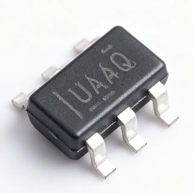
TS5A3159QDBVRQ1 - 1Ω SPDT Analog Switch AEC-Q100 | TI
MPN: TS5A3159QDBVRQ1 ✓ 啟用中| 數量 | 單價 | 小計 |
|---|---|---|
| 1 | $0.55 | $0.55 |
| 10 | $0.49 | $4.90 |
| 100 | $0.3969 | $39.69 |
| 500 | $0.33 | $165.00 |
| 1,000 | $0.28 | $280.00 |
TS5A3159QDBVRQ1 概覽
An analog switch is a semiconductor device that routes or gates analog and digital signals under the control of a logic-level input. Within the signal-chain hierarchy, the SPDT analog switch sits in the analog switches and multiplexers family, below large multiplexer arrays and alongside transmission-gate logic. An SPDT device connects one common (COM) terminal to either of two throw terminals (NO or NC), making it the fundamental building block of signal routing and redundancy switching.
Key features include break-before-make switching, which prevents momentary channel shorting during transition and eliminates signal distortion when a signal source moves between paths; an excellent total harmonic distortion (THD) specification that preserves audio and precision-signal integrity; and low ON-resistance matching and flatness, which minimize signal error across the input range.
The device operates from a single 1.65V to 5.5V supply, compatible with 1.8V, 2.5V, 3.3V, and 5V logic systems. The switch core uses a low-charge-injection MOS transmission-gate architecture with approximately 8pF typical ON capacitance (per TI family data), limiting high-frequency insertion loss in data and RF routing paths. The digital IN pin is logic compatible across the full supply range, and the -Q1 suffix denotes AEC-Q100 qualification with -40C to +125C operation for automotive environments.
Typical applications include automotive audio source selection, sensor-signal multiplexing in battery-management and body-control modules, UART/SPI/SMBus line sharing, and general-purpose signal gating in industrial systems. The 2.9mm x 1.6mm SOT-23-6 footprint suits densely populated boards.
Design tip: terminate or AC-ground unused throw terminals to reduce crosstalk, and place the device close to the signal source to minimize parasitic trace capacitance.
This page synthesizes distributor pricing, drop-in alternatives, comparison tables, and practical design notes not found in the manufacturer datasheet.
直接替換替代品,適用於 TS5A3159QDBVRQ1 — 相同封裝,腳位對腳位相容。需重新設計 PCB 的不同封裝零件不列入。
此系列的變體
與下列產品可直接替換的同系列型號: TS5A3159QDBVRQ1 (相同外形與佔位) — 差異在於 Operating Temperature, Package, THD.
快速比較工具 — 選擇替代零件進行並排比較:
TS5A3159DBVR
✅ 直接替換聯絡詢價
查看資料表 →TS5A3159ADBVR
✅ 直接替換📋 參考替代品(不在目錄中)
TS5A3159DBVT
✅ 直接替換📋 參考替代品(不在目錄中)
TS5A3159QDBVRQ1 最大額定值與電氣特性
| Configuration | 2:1 SPDT, 1 channel |
| ON-Resistance (typ) | 1 Ohm |
| ON-Resistance (max) | 1.3 Ohm |
| Supply Voltage Range | 1.65 V to 5.5 V |
| Logic Supply Compatibility | 1.8 V, 2.5 V, 3.3 V, 5 V |
| Switching Feature | Break-before-make |
| THD | Excellent (low distortion per TI product description) |
| ON Capacitance (typ) | 8 pF |
| 工作溫度 | -40C to +125C |
| Temperature Grade | Automotive (AEC-Q100) |
| 封裝 | SOT-23-6 (DBV), 6 pins |
| Package Dimensions | 2.9 mm x 1.6 mm x 1.1 mm |
| 安裝類型 | Surface Mount |
| Lead Shape | Gull-wing |
| Packaging | Tape and Reel |
| Control Input | Logic-level IN pin |
TS5A3159QDBVRQ1 腳位配置
| 腳位 1 | NO — Normally-open throw terminal |
| 腳位 2 | GND — Ground |
| 腳位 3 | COM — Common terminal connected to NO or NC per IN logic |
| 腳位 4 | IN — Logic control input selecting COM-to-NO or COM-to-NC |
| 腳位 5 | V+ — Analog supply, 1.65 V to 5.5 V |
| 腳位 6 | NC — Normally-closed throw terminal |
典型應用
TS5A3159QDBVRQ1 適用於 6 應用s: Automotive Audio Source Selection, Sensor Signal Multiplexing in BMS, UART/SPI/SMBus Line Sharing, Redundant Signal-Path Selection in Industrial Systems, Audio Accessory Detection and Jack Switching, General-Purpose Signal Gating in Test Fixtures.
Automotive Audio Source Selection
The TS5A3159QDBVRQ1 routes one of two audio sources to a common output in head units and amplifier modules. Its ~1 Ohm ON-resistance minimizes insertion loss in low-impedance audio paths, while TI's highlighted low THD preserves signal fidelity across the audio band. Break-before-make switching eliminates switching transients and source-to-source contention when changing inputs. The AEC-Q100 qualification and -40C to +125C range make it appropriate for in-vehicle environments. Place the switch near the source connectors with short traces to limit parasitic capacitance that would roll off high-frequency audio content.
推薦
Sensor Signal Multiplexing in BMS
Battery-management and body-control modules frequently share one ADC input across multiple sensor channels. The TS5A3159QDBVRQ1's 1 Ohm typ ON-resistance introduces only millivolt-level error into high-impedance sensor signals, and its low charge injection preserves measurement accuracy during channel transitions. The 1.65V to 5.5V supply range matches both 3.3V and 5V ADC reference domains common in automotive ECUs. AEC-Q100 qualification supports under-hood and cabin deployments. A short settling delay after switching - due to break-before-make plus ON-capacitance charging - should be allowed in the ADC sampling sequence.
推薦
UART/SPI/SMBus Line Sharing
When a microcontroller's serial pins must be shared between two peripherals or two bus masters, the TS5A3159QDBVRQ1 provides a clean 2:1 digital switch. The ~1 Ohm Ron is negligible against typical bus pull-ups and driver impedances, and the 8pF typ ON-capacitance preserves edge rates at common UART (115.2 kbps) and SPI (a few MHz) speeds. The logic-compatible IN pin accepts direct GPIO drive from 1.8V to 5V domains. Automotive qualification allows use in telematics and body modules. Ensure only one side drives the shared line to avoid bus contention during switchover.
推薦
Redundant Signal-Path Selection in Industrial Systems
Industrial control and instrumentation systems often provide redundant sensor or communication paths that must be switched on failure detection. The TS5A3159QDBVRQ1's break-before-make action guarantees the primary and backup paths are never momentarily connected, preventing source contention during failover. Its low Ron (1 Ohm typ) and excellent matching keep gain errors below 1% even in low-impedance signal chains, and the wide 1.65V to 5.5V supply simplifies integration into mixed-voltage PLC I/O cards. The SOT-23-6 footprint fits dense I/O modules with minimal board area overhead.
推薦
Audio Accessory Detection and Jack Switching
Mobile and automotive head-unit designs use small SPDT switches to reconfigure headset jack pins between detection, microphone, and audio functions. The TS5A3159QDBVRQ1's low THD keeps the microphone path clean, the low Ron preserves mic bias integrity, and break-before-make avoids audible pops during mode changes. The 1.65V to 5.5V supply range covers battery-powered and 5V USB-host rails. The 2.9mm x 1.6mm SOT-23-6 package fits near the jack connector where board space is tight. AC-ground unused throw terminals to reduce crosstalk into adjacent audio channels.
推薦
General-Purpose Signal Gating in Test Fixtures
Bench instruments, probe multiplexers, and automated test equipment use SPDT switches to route signals between calibration and measurement paths. The TS5A3159QDBVRQ1's low ON-capacitance (8pF typ) minimizes bandwidth degradation on routed signals, while the flat, low Ron maintains amplitude accuracy across the switch's common operating range. Supply flexibility from 1.65V to 5.5V lets one fixture design serve multiple logic-voltage products. Because test fixtures are non-automotive, the standard TS5A3159DBVR can be substituted for cost savings without layout changes thanks to the identical SOT-23-6 footprint.
推薦
推薦產品摘要
工程參考資料,適用於 TS5A3159QDBVRQ1 — 比較、設計指引及合規資訊。
選型指南
與替代品比較
| 參數 | 本產品 | TS5A3159DBVR | TS5A3159ADBVR | TS5A3159DBVT |
|---|---|---|---|---|
| Package | SOT-23-6 (DBV) | SOT-23-6 (DBV) - same | SOT-23-6 (DBV) - same | SOT-23-6 (DBV) - same |
| Brand | Texas Instruments | Texas Instruments | Texas Instruments | Texas Instruments |
| Configuration | 2:1 SPDT | 2:1 SPDT | 2:1 SPDT | 2:1 SPDT |
| Supply Voltage Range | 1.65 V to 5.5 V | 1.8 V, 2.5 V, 3.3 V, 5 V compatible | 1.8 V, 2.5 V, 3.3 V, 5 V compatible | 1.8 V, 2.5 V, 3.3 V, 5 V compatible |
| Qualification | AEC-Q100 (automotive) | Standard grade | Standard grade | Standard grade |
| Break-Before-Make | Yes | Yes | Yes | Yes |
主要差異化特點
- AEC-Q100 automotive qualification (對比TS5A3159DBVR)
- Low ON-resistance in a 6-pin package (對比TS5A3159ADBVR)
- Break-before-make switching with low THD (對比TS5A3159DBVT)
設計說明
Keep traces between the TS5A3159QDBVRQ1 and the signal source as short as possible. The switch's ~8pF typical ON-capacitance combines with trace parasitic capacitance to form a low-pass filter; long traces (roughly >50mm) on high-impedance nodes can visibly roll off fast edges or high-frequency audio content. Terminate or AC-ground the unused NO/NC terminal to reduce crosstalk into the selected channel.
Respect the break-before-make interval during switchover: do not drive the IN pin with a signal that toggles faster than the device's switching time specification, and never allow both NO and NC sources to be actively driving at the instant of transition. For precision sensor multiplexing, allow settle time after switching for the ON-capacitance to charge before triggering the ADC sample.
Decouple V+ (pin 5) with a 100nF ceramic capacitor placed within a few millimeters of the pin, with a solid ground return via pin 2. The SOT-23-6 package has no exposed pad, so the ground connection relies solely on pin 2 - use a short, wide trace or via to the ground plane. Place the device close to the signal source to minimize parasitic trace capacitance and charge-injection effects on sensitive nodes.
合規資訊
AEC-Q100 automotive qualification confirmed by the -Q1 suffix and TI/Arrow product data. RoHS/REACH/lead-free status not stated in provided data - verify on TI product page quality section.




