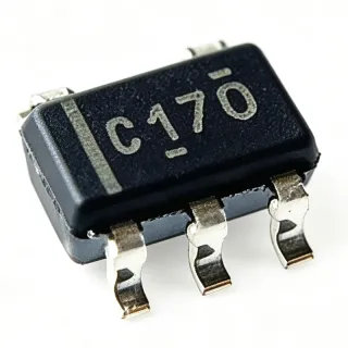
SN74LVC1G125QDBVRQ1 - AEC-Q100 Buffer, 3-State, SOT-23-5 | TI
MPN: SN74LVC1G125QDBVRQ1 ✓ 啟用中SN74LVC1G125QDBVRQ1 概覽
A single-bus buffer gate is a logic device in the voltage-level and drive-strength hierarchy of digital ICs: buffer gate -> line driver -> bus-interface logic. Its role is to restore signal edges, increase fan-out, and isolate bus segments without inverting logic polarity.
Key features include 5.5V-tolerant inputs for mixed-voltage environments, high output drive from advanced CMOS technology, and robust ESD protection rated at 2000V HBM, 200V MM, and 1000V CDM per the datasheet. The Q1 suffix denotes AEC-Q100 qualification and customer-specific configuration control, making the device suitable for automotive body, cluster, and infotainment modules.
Fabricated on TI's advanced CMOS LVC process, the buffer achieves high speed with low power consumption and balanced drive in both push-pull directions. The NanoStar/NanoFree small-footprint SOT-23-5 package supports dense PCB layouts while maintaining 5V VCC operation capability.
Typical applications include automotive CAN/LIN module I/O buffering, level-compatible bus isolation at 3.3V and 5V, MCU GPIO line driving, and sensor signal gating in 12V automotive electronic control units.
Design tip: tie the OE pin to GND for a permanently enabled buffer; never leave OE floating, as the active-low enable polarity differs from the SN74LVC1G126 variant.
直接替換替代品,適用於 SN74LVC1G125QDBVRQ1 — 相同封裝,腳位對腳位相容。需重新設計 PCB 的不同封裝零件不列入。
此系列的變體
與下列產品可直接替換的同系列型號: SN74LVC1G125QDBVRQ1 (相同外形與佔位) — 差異在於 Output Enable, Output Type, RoHS Status.
SN74LVC1G125DBVR
✅ 直接替換聯絡詢價
查看資料表 →SN74LVC1G126QDBVRQ1
⚡ 相同封裝 ⚠️ 規格未經驗證📋 參考替代品(不在目錄中)
SN74AUP1T34-Q1
⚡ 相同封裝 ⚠️ 規格未經驗證聯絡詢價
查看資料表 →74LVC1G125Q-7
✅ 直接替換📋 參考替代品(不在目錄中)
74LVC1G125GV,125
✅ 直接替換 ⚠️ 規格未經驗證📋 參考替代品(不在目錄中)
SN74LVC1G125QDBVRQ1 最大額定值與電氣特性
| Logic Function | Single non-inverting buffer with 3-state output |
| Supply Voltage Range | 1.65 V to 5.5 V |
| Input Tolerance | 5.5 V tolerant inputs |
| Output Enable | OE active-low (output Hi-Z when OE HIGH) |
| 輸出類型 | 3-state push-pull |
| Automotive Qualification | AEC-Q100 qualified (Q1) |
| ESD HBM | 2000 V |
| ESD MM | 200 V |
| ESD CDM | 1000 V |
| Technology | Advanced CMOS (LVC) |
| 封裝 | SOT-23-5 (DBV) |
| 安裝類型 | Surface Mount |
| RoHS 狀態 | Compliant |
SN74LVC1G125QDBVRQ1 腳位配置
| 腳位 1 | OE — Output enable, active low (output Hi-Z when HIGH) |
| 腳位 2 | GND — Ground |
| 腳位 3 | A — Data input (5.5V tolerant) |
| 腳位 4 | Y — 3-state non-inverting output |
| 腳位 5 | VCC — Power supply, 1.65V to 5.5V |
典型應用
SN74LVC1G125QDBVRQ1 適用於 6 應用s: Automotive Body Electronics ECU, Mixed-Voltage Level Compatible Buffering, Instrument Cluster Display Logic, Battery Management System I/O Gating, Industrial Automation Control Logic, Telematics and Gateway Modules.
Automotive Body Electronics ECU
In body control modules and automotive ECUs, the SN74LVC1G125QDBVRQ1 buffers MCU GPIO signals driving switch inputs, relay logic, and lamp-check lines. Its AEC-Q100 qualification makes it suitable for harsh cabin and under-hood electronics where commercial logic is not permitted. The 1.65V-5.5V VCC range lets the same design re-use the part across 3.3V and 5V subsystems, and 2000V HBM ESD tolerance withstands automotive assembly handling. Placed as a 3-state line driver, the OE pin lets the MCU tri-state sensor buses during diagnostics, isolating faulty nodes without relays.
推薦
Mixed-Voltage Level Compatible Buffering
The 5.5V-tolerant inputs of the SN74LVC1G125QDBVRQ1 make it a simple one-gate solution in mixed-voltage systems where a 5V legacy signal must gate a 3.3V rail, or vice versa. Powered at 1.65V-5.5V, the input never sees overstress even at 5V signals with VCC lowered, unlike non-tolerant LVC inputs. The 3-state output provides bus isolation during power-up sequencing - asserting OE HIGH tri-states the driver while downstream rails settle. This is frequently used to gate SPI chip-select or enable lines crossing voltage domains in automotive and industrial controllers.
推薦
Instrument Cluster Display Logic
Cluster and dashboard modules use the SN74LVC1G125QDBVRQ1 to buffer display-backlight enables, stepper-motor pointer control signals, and indicator LED drive gating. The high output drive from TI's advanced CMOS LVC process restores slow, attenuated edges across long harness-driven PCB traces, and the push-pull 3-state output can be parked in Hi-Z when the display subsystem is powered down. AEC-Q100 qualification and customer-specific configuration control satisfy OEM change-management requirements for tier-1 cluster suppliers, while SOT-23-5 fits dense cluster PCBs.
推薦
Battery Management System I/O Gating
In BMS slave boards, the SN74LVC1G125QDBVRQ1 gates cell-monitor daisy-chain control and diagnostic select lines. The 3-state output enables shared single-wire diagnostic buses: multiple buffers connect to one line with only one OE asserted LOW at a time, preventing contention. The 1.65V-5.5V supply matches both 3.3V monitoring ICs and 5V communication ports, and the Q1 automotive grade is required in EV traction-battery environments. The active-low OE also naturally fits watchdog-driven enable logic where a HIGH (fault) state must force Hi-Z.
推薦
Industrial Automation Control Logic
In PLC I/O cards and factory automation boards, the buffer restores fan-out-degraded signals from counters, encoder comparators, and optocoupler outputs. Where an industrial variant is acceptable, the same-die SN74LVC1G125DBVR offers a lower-cost path; the Q1 version suits industrial equipment sharing a qualified BOM with automotive lines. The 3-state output supports bus-organized I/O backplanes where multiple cards drive a shared status line. 2000V HBM ESD robustness is valuable near connector edges where field wiring induced transients are handled upstream by TVS diodes.
推薦
Telematics and Gateway Modules
Automotive telematics gateways use the SN74LVC1G125QDBVRQ1 to gate cellular-module PWRKEY and reset-control lines and to buffer GPIO between the main SoC and CAN/LIN transceivers. The OE pin allows the MCU to release control lines during module firmware updates, matching the 3-state bus discipline required by shared boot-strap pins. With 5.5V-tolerant inputs, the buffer safely interfaces 5V-tolerant transceiver I/O even while its own rail is 3.3V, eliminating a level-shifting stage and saving board area in space-constrained gateway designs.
推薦
推薦產品摘要
工程參考資料,適用於 SN74LVC1G125QDBVRQ1 — 比較、設計指引及合規資訊。
選型指南
與替代品比較
| 參數 | 本產品 | SN74LVC1G125DBVR | 74LVC1G125Q-7 | 74LVC1G125GV,125 |
|---|---|---|---|---|
| Package | SOT-23-5 (DBV) | SOT-23-5 (DBV) - same | SOT-23-5 - same | SOT-23-5 - same |
| Brand | Texas Instruments | Texas Instruments | Diodes Incorporated | Nexperia |
| Supply Voltage Range | 1.65 V to 5.5 V | 1.65 V to 5.5 V | 1.65 V to 5.5 V | 1.65 V to 5.5 V |
| Output Enable Polarity | Active-low (Hi-Z when OE HIGH) | Active-low | Active-low | Active-low |
| Input Tolerance | 5.5 V tolerant | 5.5 V tolerant | 5.5 V tolerant | 5.5 V tolerant |
主要差異化特點
- AEC-Q100 automotive qualification (對比SN74LVC1G125DBVR)
- Automotive-compliant cross-brand second source (對比74LVC1G125Q-7)
- Active-low OE bus discipline (對比SN74LVC1G126QDBVRQ1)
設計說明
Do not confuse OE polarity with the SN74LVC1G126: on the G125, output is enabled when OE is LOW and Hi-Z when OE is HIGH. Substituting a G126 without checking OE logic causes permanent bus contention or tri-state. Also never leave OE floating - tie to GND via 0-ohm/10k pull-down for a permanently enabled buffer.
Place a 0.1uF ceramic decoupling capacitor within 2-3 mm of VCC (pin 5) to GND. Keep the A-to-Y trace short for clean edge propagation, and route OE away from switching nodes to avoid glitch-induced tri-stating. The SOT-23-5 footprint (DBV) is standard and allows direct placement of pin-compatible alternatives.
Use the 5.5V input tolerance deliberately: the input may be driven to 5.5V regardless of VCC, but keep VCC within 1.65V-5.5V. In mixed-voltage boards, ensure OE is not asserted from an unpowered voltage domain to avoid back-powering through input protection structures during power sequencing.
合規資訊
Q1 suffix denotes AEC-Q100 automotive qualification per TI product page. RoHS/lead-free per standard TI SMD packaging for active catalog parts.