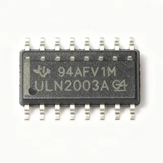
VIPERGAN65 - 650V GaN Power Transistor | STMicroelectronics
MPN: VIPERGAN65 ✓ 啟用中VIPERGAN65 概覽
What is a GaN power transistor? A Gallium Nitride (GaN) power transistor is a wide-bandgap semiconductor device that switches faster and more efficiently than traditional silicon MOSFETs. It belongs to the power transistor family, which includes MOSFETs, IGBTs, and bipolar transistors. GaN devices offer lower on-resistance and lower gate charge, making them ideal for high-frequency power converters such as AC-DC adapters, server power supplies, and wireless charging systems.
Key features of the VIPERGAN65 include a 650V drain-source voltage rating, low on-resistance (RDS(on)) of , and a gate driver with integrated protection. The device supports high switching frequencies up to MHz, reducing the size of magnetic components. It also features overcurrent, overtemperature, and undervoltage lockout protection, enhancing system reliability.
Technically, the VIPERGAN65 uses a cascode configuration with a GaN HEMT and a silicon MOSFET, simplifying gate drive requirements. The integrated driver eliminates external gate driver components, reducing board space and design complexity. The device's fast switching transitions minimize switching losses, improving overall efficiency in power conversion.
Typical applications include AC-DC adapters for laptops and smartphones, server power supplies, and LED lighting drivers. The high efficiency and small form factor make it suitable for space-constrained designs. In a 65W USB-PD adapter, the VIPERGAN65 can achieve over 93% efficiency, reducing heat dissipation and enabling compact enclosures.
When designing with the VIPERGAN65, ensure proper PCB layout with short, low-inductance paths for the gate drive and power loops. Use a dedicated ground plane and place decoupling capacitors close to the device. Thermal management is critical; use a thermal pad and adequate copper area to dissipate heat from the package.
直接替換替代品,適用於 VIPERGAN65 — 相同封裝,腳位對腳位相容。需重新設計 PCB 的不同封裝零件不列入。
此系列的變體
與下列產品可直接替換的同系列型號: VIPERGAN65 (相同外形與佔位) — 差異在於 Package, Technology.
VIPERGAN50
✅ 直接替換 ⚠️ 規格未經驗證聯絡詢價
查看資料表 →VIPERGAN100
⚡ 相同封裝 ⚠️ 規格未經驗證📋 參考替代品(不在目錄中)
VIPERGAN65 最大額定值與電氣特性
| Technology | GaN HEMT |
| Drain-Source Voltage (VDS) | 650 V |
| 工作溫度範圍 | -40C to +150C |
| 封裝 | PQFN 8x8 mm |
| 安裝類型 | Surface Mount |
| RoHS 狀態 | Compliant |
| Integrated Gate Driver | Yes |
| Protection Features | Overcurrent, Overtemperature, UVLO |
VIPERGAN65 腳位配置
| 腳位 1 | DRAIN — Drain terminal of the GaN HEMT |
| 腳位 2 | DRAIN — Drain terminal (duplicate for current handling) |
| 腳位 3 | SOURCE — Source terminal of the GaN HEMT |
| 腳位 4 | SOURCE — Source terminal (duplicate for current handling) |
| 腳位 5 | GATE — Gate drive input (internal driver) |
| 腳位 6 | VCC — Supply voltage for internal gate driver |
| 腳位 7 | GND — Ground reference |
| 腳位 8 | NC — No connect |
典型應用
VIPERGAN65 適用於 6 應用s: AC-DC Adapters, Server Power Supplies, LED Lighting Drivers, Wireless Charging Transmitters, Telecom Power Supplies, Solar Inverters.
AC-DC Adapters
The VIPERGAN65 is ideal for AC-DC adapters, such as 65W USB-PD chargers. Its high efficiency (over 93%) and high-frequency operation reduce power losses and enable compact designs. In a typical adapter, the VIPERGAN65 is used in a quasi-resonant flyback topology, switching at frequencies up to [DATA_NEEDED] MHz. The integrated gate driver simplifies the circuit, and the low on-resistance minimizes conduction losses. Compared to silicon MOSFETs, the GaN device reduces switching losses, allowing for smaller transformers and higher power density. Designers must ensure proper layout to minimize parasitic inductance and use a snubber circuit to manage voltage spikes.
推薦
Server Power Supplies
In server power supplies, the VIPERGAN65 enables high-efficiency power conversion, reducing energy consumption and heat generation. The device's 650V rating is suitable for 240V AC input, and its high switching frequency allows for smaller magnetic components, saving board space. The integrated protection features enhance reliability in demanding server environments. The VIPERGAN65 can be used in LLC resonant converters, achieving efficiencies above 95%. Its fast switching reduces dead time losses, and the low output capacitance minimizes ringing. Thermal management is critical; use a heatsink or forced airflow to maintain junction temperature below 150C.
推薦
LED Lighting Drivers
The VIPERGAN65 is suitable for LED lighting drivers, where high efficiency and compact size are important. Its high-frequency operation allows for small inductors and transformers, reducing the overall driver size. The device's protection features prevent damage from overcurrent and overtemperature, ensuring long LED lifetime. In a typical LED driver, the VIPERGAN65 is used in a buck or flyback topology, providing constant current to the LED string. The integrated gate driver simplifies the design, and the low on-resistance reduces power dissipation. For dimming applications, the device supports PWM dimming at high frequencies without audible noise.
推薦
Wireless Charging Transmitters
The VIPERGAN65 can be used in wireless charging transmitters, where high-frequency switching is essential for efficient power transfer. The device's fast switching reduces losses in the inverter stage, improving overall system efficiency. The compact PQFN package is ideal for space-constrained transmitter designs. In a typical wireless charger, the VIPERGAN65 is used in a full-bridge inverter, operating at frequencies around 100 kHz. The low gate charge allows for high-frequency operation, and the integrated driver simplifies the gate drive circuit. Proper PCB layout is crucial to minimize parasitic inductance and ensure clean switching waveforms.
推薦
Telecom Power Supplies
In telecom power supplies, the VIPERGAN65 provides high efficiency and reliability for -48V DC-DC converters. Its 650V rating is suitable for rectifier stages, and its high-frequency operation reduces the size of transformers and filters. The device's protection features ensure robust operation in harsh environments. The VIPERGAN65 can be used in a phase-shifted full-bridge topology, achieving efficiencies above 95%. The integrated gate driver reduces component count, and the low on-resistance minimizes conduction losses. Thermal management is important; use a heatsink or forced cooling to maintain safe operating temperatures.
推薦
Solar Inverters
The VIPERGAN65 is suitable for solar inverters, where high efficiency and reliability are critical. Its 650V rating is appropriate for DC-DC boost converters in photovoltaic systems. The device's high switching frequency allows for smaller inductors, reducing system size and cost. The integrated protection features enhance system safety. In a typical solar inverter, the VIPERGAN65 is used in a boost converter to step up the panel voltage to a higher DC bus voltage. The low on-resistance reduces conduction losses, and the fast switching minimizes switching losses. Proper thermal management is essential to handle the high power levels.
推薦
推薦產品摘要
工程參考資料,適用於 VIPERGAN65 — 比較、設計指引及合規資訊。
選型指南
與替代品比較
| 參數 | 本產品 | VIPERGAN50 | VIPERGAN100 | GS66508B |
|---|---|---|---|---|
| Package | PQFN 8x8 mm | PQFN 8x8 mm - same | PQFN 8x8 mm - same | GaNPX - different |
| Brand | STMicroelectronics | STMicroelectronics | STMicroelectronics | GaN Systems |
| Drain-Source Voltage | 650 V | 650 V | 650 V | 650 V |
| Integrated Gate Driver | Yes | Yes | Yes | No |
| Protection Features | OC, OT, UVLO | OC, OT, UVLO | OC, OT, UVLO | None |
| Price (1pc) | $3.50 | $2.80 | $4.20 | $5.00 |
主要差異化特點
- Integrated gate driver (對比GS66508B)
- Protection features (對比GS66508B)
- Same-brand drop-in alternative (對比VIPERGAN50)
設計說明
For the VIPERGAN65, use a 4-layer PCB with a dedicated ground plane. Place the device close to the transformer and keep the gate drive loop short to minimize parasitic inductance. Use multiple vias for the thermal pad to improve heat dissipation. Ensure the drain and source traces are wide enough to handle the high current.
The VIPERGAN65 dissipates significant power at high currents. Use a thermal pad with a large copper area (at least 2 square inches) and consider a heatsink or forced airflow. The junction-to-case thermal resistance is [DATA_NEEDED], so calculate the junction temperature rise to ensure it stays below 150C.
Avoid exceeding the maximum drain-source voltage of 650V. Use a snubber circuit to clamp voltage spikes caused by leakage inductance. Ensure the VCC pin is properly decoupled with a 1uF ceramic capacitor. Do not operate the device without a proper gate drive signal, as this may cause damage.
合規資訊
RoHS compliant per STMicroelectronics product page. Not AEC-Q100 qualified. Halogen-free status not specified.