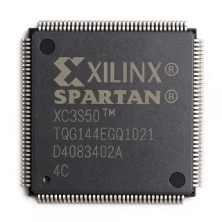
XA3S200-4TQG144I - 4320-Logic-Cell Spartan-3 XA FPGA | AMD
MPN: XA3S200-4TQG144I ✗ 停產XA3S200-4TQG144I 概覽
A field-programmable gate array, or FPGA, is a semiconductor whose digital logic, memory, and I/O can be configured after manufacture. An FPGA belongs to the programmable-logic hierarchy, where it complements ASICs, microcontrollers, and DSP processors. Its parallel configurable resources allow multiple digital functions to be consolidated into one device, reducing component count while shortening development cycles for prototype and production systems.
The XA3S200-4TQG144I provides 4,320 logic elements organized as 1,920 adaptive logic modules. Its 216 kbit of embedded block RAM supports data buffers, packet storage, lookup tables, and small local memories without external memory. The 97 available I/O give designers access to interfaces for control, communications, instrumentation, industrial control, embedded processing, and general-purpose digital interfaces. Its 144-LQFP package provides a standard gull-wing surface-mount footprint with 144 terminals.
The Spartan-3 XA family targets automotive and industrial programmable-logic requirements while retaining the familiar Spartan-3 architecture. Its integrated I/O resources support seventeen single-ended signal standards, seven differential standards including LVDS, and digitally controlled impedance termination. These features are useful when a board must interface reliably to external logic, communications transceivers, sensors, or memory across varying signal-loading conditions.
Typical designs include industrial controllers, data-acquisition systems, embedded communications gateways, video-processing pipelines, automotive electronic modules, and general embedded control platforms. The FPGA is particularly useful when parallel architecture, deterministic timing, configurable I/O, and field-updatable logic are more valuable than the low power and simplicity of a fixed-function microcontroller.
Designers should use the AMD Spartan-3 XA product specification, pinout tables, and configuration guidance when assigning pins and selecting I/O standards. Validate signal-integrity and power-integrity requirements across temperature, voltage, and process corners, and confirm that board-level memory, clocking, configuration, and programming interfaces support the intended system architecture.
This product summary combines package, resource, interface, comparison, and design information to simplify initial component selection while directing engineers to the authoritative AMD documentation for implementation details.
直接替換替代品,適用於 XA3S200-4TQG144I — 相同封裝,腳位對腳位相容。需重新設計 PCB 的不同封裝零件不列入。
此系列的變體
與下列產品可直接替換的同系列型號: XA3S200-4TQG144I (相同外形與佔位) — 差異在於 Package, Temperature Grade.
XA3S200-4TQG144Q
✅ 直接替換聯絡詢價
XC3S200-4TQG144I
✅ 直接替換📋 參考替代品(不在目錄中)
XC3S200-4TQG144C
✅ 直接替換📋 參考替代品(不在目錄中)
XA3S200-4TQG144C
✅ 直接替換 ⚠️ 規格未經驗證📋 參考替代品(不在目錄中)
XA3S200-5TQG144I
✅ 直接替換 ⚠️ 規格未經驗證📋 參考替代品(不在目錄中)
XA3S200-4TQG144I 最大額定值與電氣特性
| Device Type | Spartan-3 XA field-programmable gate array |
| System Gates | 200,000 gates |
| Logic Cells | 4,320 logic cells |
| Adaptive Logic Modules | 1,920 ALMs |
| Logic Blocks | 480 logic blocks |
| Embedded Memory | 216 kbit |
| User I/O | 97 I/O |
| Maximum Data Rate per I/O | 622 Mb/s |
| Single-Ended Signal Standards | 17 standards |
| Differential Signal Standards | 7 standards, including LVDS |
| Core Supply Voltage | 1.2 V |
| Temperature Grade | Industrial |
| 封裝 | 144-LQFP |
| Package Terminal Count | 144 terminals |
| Package Form | Square gull-wing surface-mount package |
XA3S200-4TQG144I square gull-wing surface-mount package 腳位配置指南
XA3S200-4TQG144I(square gull-wing surface-mount package 封裝)的腳位配置。 此數位 IC 包含 GPIO、通訊介面(UART、SPI、I2C)與電源腳位。替代腳位功能與配置選項請參閱製造商資料表。對嵌入式系統設計與 PCB 佈局至關重要。

無詳細腳位定義資料: XA3S200-4TQG144I.
請參閱 資料表 以查看完整腳位配置。
典型應用
XA3S200-4TQG144I 適用於 6 應用s: Industrial Control and Automation, Automotive Electronic Control, Data Acquisition and Instrumentation, Communications Gateway, Embedded Video Processing, Programmable Signal Processing.
Industrial Control and Automation
The XA3S200-4TQG144I fits industrial controllers that combine parallel logic, local memory, and numerous digital control interfaces. Its 4,320 logic cells and 1,920 adaptive logic modules can implement state machines, timers, interlocks, protocol engines, and motion-control sequencing, while 216 kbit of embedded block RAM supports local buffers and history records. The 97 user I/O provide capacity for sensors, actuators, safety-oriented logic isolation, and communications peripherals. In a controller, the FPGA can execute multiple timing-critical functions in parallel and reduce reliance on discrete logic. Use the AMD product specification to confirm bank voltage, clock topology, configuration requirements, and temperature limits.
推薦
Automotive Electronic Control
The Spartan-3 XA XA3S200-4TQG144I is appropriate for programmable automotive electronic modules requiring parallel real-time logic, configurable I/O, and an industrial-temperature ordering option. The FPGA can consolidate sensor conditioning logic, actuator timing, communication routing, and diagnostic functions in one package. Seventeen single-ended and seven differential I/O standards, including LVDS, help support links to sensors and transceivers, while 216 kbit of embedded memory enables local buffering and protocol processing. The 97 I/O provide substantial board-level connectivity. Confirm exact AEC-Q100 status, automotive qualification requirements, transient protection, and operating-temperature limits for the production design before release.
推薦
Data Acquisition and Instrumentation
The XA3S200-4TQG144I is well suited to parallel data-acquisition front ends where multiple inputs must be sampled, filtered, and transferred deterministically. Its 4,320 logic elements can implement acquisition state machines, trigger logic, digital filtering, and data-format conversion, while the 216 kbit of embedded RAM can buffer bursts between the analog or digital front end and a communications engine. Up to 622 Mb/s per I/O supports demanding interfaces when board-level timing and signal integrity permit. Digitally controlled impedance is useful on controlled-impedance boards. Validate input thresholds, bank supplies, clock jitter, termination, and timing closure for the selected sensor and converter interfaces.
推薦
Communications Gateway
The XA3S200-4TQG144I can serve as a flexible gateway for protocols and data paths that benefit from deterministic parallel logic. Its programmable resources can implement framing, packet filtering, byte alignment, buffering, and error detection across multiple interfaces, while 216 kbit of embedded block RAM supports local packet queues and protocol tables. The 97 I/O and range of single-ended and differential standards allow connection to transceivers and serializers, including LVDS links. Place clock and I/O planning constraints ahead of logic assignment because package resources and supported standards depend on voltage banks and adjacent signals. Confirm configuration, clocking, and I/O specifications against the AMD documentation before finalizing the gateway design.
推薦
Embedded Video Processing
The XA3S200-4TQG144I can support parallel video-format conversion, timing generation, filtering, and interface bridging in compact embedded systems. The 4,320 logic cells provide parallel resources for pixel routing and control, and 216 kbit of embedded RAM can hold line buffers, lookup data, or compact frame-processing stages. Its 97 I/O provide substantial connectivity to sensors, display interfaces, and serializers, while the 622 Mb/s-per-I/O figure supports high-speed transfers when timing closure and board constraints are satisfied. The design should account for clock-domain crossings, pixel-clock jitter, output timing, and memory bandwidth. Use the AMD I/O and timing resources to select voltage standards and verify all external video interfaces.
推薦
Programmable Signal Processing
The XA3S200-4TQG144I is useful for fixed-latency digital filtering, modulation, correlation, and custom signal-processing functions that map efficiently to parallel FPGA resources. Multiple logic pipelines can execute concurrently, and the 216 kbit of embedded block RAM provides local coefficient, delay-line, or sample storage without relying entirely on external memory. The 97 I/O support parallel converters, digital sensors, clocks, and high-speed links. Because block RAM bandwidth, clock frequency, and routing can constrain throughput, estimate resource utilization before committing to a sample rate or channel count. Confirm industrial temperature performance, timing margins, clock jitter tolerance, and I/O standards for each production operating condition.
推薦
推薦產品摘要
工程參考資料,適用於 XA3S200-4TQG144I — 比較、設計指引及合規資訊。
選型指南
與替代品比較
| 參數 | 本產品 | XA3S200-4TQG144Q | XC3S200-4TQG144I | XC3S200-4TQG144C | XA3S200-4TQG144C | XA3S200-5TQG144I |
|---|---|---|---|---|---|---|
| Package | 144-LQFP | 144-LQFP | 144-LQFP | 144-LQFP | 144-LQFP | 144-LQFP |
| Brand | AMD | AMD | AMD | AMD | AMD | AMD |
| FPGA Family | Spartan-3 XA | Spartan-3 XA | Spartan-3 | Spartan-3 | Spartan-3 XA | Spartan-3 XA |
| Logic Elements | 4,320 | 4,320 | 4,320 | 4,320 | 4,320 | 4,320 |
| User I/O | 97 I/O | 97 I/O | 97 I/O | 97 I/O | 97 I/O | 97 I/O |
| Speed Designation | -4 | -4 | -4 | -4 | -4 | -5 |
| Core Supply Voltage | 1.2 V | 1.2 V | 1.2 V | 1.2 V | 1.2 V | 1.2 V |
主要差異化特點
- Retains the XA3S200 industrial-grade resource configuration (對比XA3S200-4TQG144Q)
- Provides the same principal resource counts as the original Spartan-3 option (對比XC3S200-4TQG144I)
- Industrial temperature selection avoids the commercial-temperature limitation (對比XC3S200-4TQG144C)
- Maintains the -4 speed grade while offering a same-family higher-speed ordering option (對比XA3S200-5TQG144I)
設計說明
Design the power rails from the AMD Spartan-3 XA electrical-characteristics tables before assigning I/O standards. The FPGA has a 1.2 V core supply, while user I/O may require other bank voltages. Use separate, adequately decoupled core and I/O supplies, place bulk and high-frequency decoupling capacitors near the relevant supply pins, and verify sequencing against the device requirements. This is particularly important when mixing single-ended, differential, or LVDS interfaces across multiple banks.
Use the exact TQG144 package-pin table to assign power, configuration, clock, and user signals; pin names and bank assignments must not be inferred from another 144-LQFP FPGA. Reserve differential pairs according to the AMD package-pin guidance, route clocks as controlled-impedance nets, and keep high-speed I/O away from noisy analog or switching sections. A pin-compatible family member still requires design verification for configuration pins, bank voltages, and I/O standards.
The documented maximum of 622 Mb/s per I/O is a device capability, not a guaranteed board result. Base trace geometry, layer stack-up, connectors, vias, and external circuitry on the selected I/O standard and edge rate. Use source-synchronous clocking where applicable, apply controlled impedance and LVDS termination according to the AMD interface guidance, and verify timing and signal integrity with simulation or measurement across voltage and temperature corners.
Do not treat a matching package as proof that any same-package FPGA is a drop-in replacement. Confirm configuration interface, power sequencing, bank voltages, pin functions, performance grade, temperature range, qualification, and bitstream compatibility. In particular, commercial C-grade options are not equivalent to industrial I-grade operation, and original Spartan-3 XC devices differ from Spartan-3 XA devices even when their published resource counts match.
合規資訊
The AMD Spartan-3 XA documentation identifies an automotive device family, but exact-device RoHS, REACH, AEC-Q100, lead-free, halogen-free, and conflict-minerals status were not established. Confirm these requirements for the ordered part and manufacturing configuration.