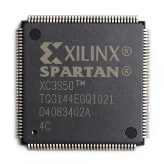
XC6SLX9-3TQG144C - 9,152-LC Spartan-6 LX FPGA | AMD
MPN: XC6SLX9-3TQG144C ✗ 停產XC6SLX9-3TQG144C 概覽
An FPGA is a programmable semiconductor in the broader logic and semiconductor hierarchy. Unlike a fixed-function microcontroller or application-specific integrated circuit, an FPGA combines configurable logic blocks, programmable interconnect, block RAM, and dedicated input/output resources on one device. The Spartan-6 LX family targets low-cost designs while retaining the flexibility to implement control logic, protocol handling, data acquisition, and hardware acceleration.
The verified listing identifies 102 I/O, 589824 embedded-memory bits, 9152 logic cells, and a 144-LQFP package. The -3 suffix denotes the highest-performance speed grade in the supplied Spartan-6 comparison information. A separate search result reports a 667 MHz internal frequency and a 0 to 85 C operating-temperature range, but those values require confirmation against the appropriate official device data before final design release.
Typical uses include industrial automation, motor control, machine-vision interfaces, sensor acquisition, protocol conversion, communication infrastructure, and embedded control systems. The package exposes 144 pins for power, ground, configuration, clock, and user-I/O connections. Exact pin names, bank voltage limits, configuration pins, and package dimensions were not supplied in the verified excerpts and must be taken from the official AMD Spartan-6 package pinout files.
For a new design, use the AMD package pinout file and the device-specific Spartan-6 documentation before assigning pins. Confirm that every powered bank, configuration signal, clock source, and I/O standard satisfies the design's voltage and timing requirements. The mature 45 nm Spartan-6 architecture is also supported by established FPGA tool flows, although tool-version and device-support details should be verified separately.
直接替換替代品,適用於 XC6SLX9-3TQG144C — 相同封裝,腳位對腳位相容。需重新設計 PCB 的不同封裝零件不列入。
此系列的變體
與下列產品可直接替換的同系列型號: XC6SLX9-3TQG144C (相同外形與佔位) — 差異在於 Operating Temperature, RoHS Status, Logic Cells, Package, Process Technology.
XC6SLX9-3TQG144I
✅ 直接替換聯絡詢價
查看資料表 →XC6SLX9-2TQG144C
✅ 直接替換聯絡詢價
查看資料表 →XC6SLX9-2TQG144I
✅ 直接替換聯絡詢價
查看資料表 →XC6SLX9-3TQG144C 最大額定值與電氣特性
| Device Type | Spartan-6 LX FPGA |
| Logic Cells | 9,152 |
| User I/O | 102 |
| Embedded Memory | 589,824 bits |
| Speed Grade | -3 |
| 封裝 | 144-LQFP |
| Package Pin Count | 144 pins |
| Internal Frequency | 667 MHz |
| 工作溫度 | 0 to 85 C |
| Lead-Free Status | Lead Free |
| RoHS 狀態 | RoHS Compliant |
| FPGA Architecture | Spartan-6 LX |
| Programmability | Field-programmable logic |
| Process Technology | 45 nm low-power copper |
| DigiKey Availability Statement | Buy now, ships today |
| Datasheet Availability | Manufacturer and distributor datasheet pages available |
XC6SLX9-3TQG144C 144 pins 腳位配置指南
XC6SLX9-3TQG144C(144 pins 封裝)的腳位配置。 此數位 IC 包含 GPIO、通訊介面(UART、SPI、I2C)與電源腳位。替代腳位功能與配置選項請參閱製造商資料表。對嵌入式系統設計與 PCB 佈局至關重要。

無詳細腳位定義資料: XC6SLX9-3TQG144C.
請參閱 資料表 以查看完整腳位配置。
典型應用
XC6SLX9-3TQG144C 適用於 6 應用s: Industrial Motor Control, Machine-Vision Interface, Sensor Data Acquisition, Protocol Conversion, Communication Infrastructure, Embedded Control Platform.
Industrial Motor Control
The XC6SLX9-3TQG144C fits cost-sensitive industrial motor-control systems that need deterministic sequencing, digital command decoding, and sensor feedback handling. Its 9,152 logic cells provide room for control state machines and supervisory logic, while 102 user I/O can support digital encoders, limit switches, interlocks, and actuator commands when voltage standards match the selected bank configuration. The -3 speed grade is useful when timing margins are important, but the design must verify actual clocking, PWM placement, and I/O timing in the FPGA tool flow. Use isolated drivers and protection networks for motor power stages rather than driving loads directly from FPGA pins.
推薦
Machine-Vision Interface
The XC6SLX9-3TQG144C is suitable for front-end machine-vision control when the FPGA must combine image-line timing, parallel sensor capture, exposure control, and data transfer. The Spartan-6 LX device's 9,152 logic cells can implement timing controllers and interface state machines, while 102 I/O offers flexibility for parallel cameras, FPGA Mezzanine Connector-style links, or control signals. The available data does not specify a particular transceiver or image-sensor interface, so LVDS, sub-LVDS, and voltage standards must be confirmed against the exact AMD I/O specifications. Validate bandwidth, clock uncertainty, and resource utilization before selecting the device.
推薦
Sensor Data Acquisition
The XC6SLX9-3TQG144C can serve as the digital control and acquisition hub for sensors that produce parallel, low-speed, or moderately sampled data. Its 102 user I/O supports multiple digital sensor channels, while embedded memory can buffer samples or support packet assembly. The 144-LQFP package is convenient for a compact controller board, but external analog front ends still determine signal integrity and accuracy. Engineers should define sampling clocks, input thresholds, debouncing, calibration, and data framing in the hardware design, then confirm operating-temperature and I/O-bank requirements against the official AMD documentation.
推薦
Protocol Conversion
The XC6SLX9-3TQG144C is appropriate for compact protocol-conversion and gateway modules where serial or parallel interfaces must be translated without a high-performance processor. Programmable logic can implement framing, CRC generation, buffering, and state-machine control, while 589,824 embedded-memory bits provide local storage for packets and status information. The exact supported protocols, baud rates, and electrical standards are not present in the supplied excerpts, so designers must select companion transceivers and validate protocol timing. Keep high-speed routing short, provide proper termination, and confirm that each external interface's voltage is compatible with the selected FPGA I/O bank.
推薦
Communication Infrastructure
The XC6SLX9-3TQG144C can support low-cost communication equipment that requires parallel-to-serial conversion, channel control, status monitoring, and programmable timing. The Spartan-6 LX architecture combines configurable logic and memory in a 144-LQFP package, allowing a compact board-level implementation without a separate high-end processor. Its suitability depends on the required channel count, data rate, clocking architecture, and I/O standards. Use the AMD package pinout file to preserve high-speed pin assignments and validate signal integrity with the selected transceiver and connector. For deployment, check lifecycle availability and temperature grade against the product's environmental requirements.
推薦
Embedded Control Platform
The XC6SLX9-3TQG144C works well as the programmable control core of an embedded platform that needs deterministic digital behavior, moderate logic density, and flexible I/O. Engineers can implement boot control, watchdog supervision, state machines, communication services, and small hardware accelerators in the FPGA fabric. The 9,152 logic cells and 102 I/O are meaningful for compact systems, but resource utilization must be checked after synthesis and implementation. The supplied data does not define configuration memory, clock pins, or bank voltage limits; obtain those details from AMD documentation and confirm that the selected toolchain supports the exact device and package.
推薦
推薦產品摘要
工程參考資料,適用於 XC6SLX9-3TQG144C — 比較、設計指引及合規資訊。
選型指南
與替代品比較
| 參數 | 本產品 | XC6SLX9-3TQG144I | XC6SLX9-2TQG144C | XC6SLX9-2TQG144I |
|---|---|---|---|---|
| Package | 144-LQFP | 144-LQFP | 144-TQG144 | 144-TQG144 |
| Brand | AMD | AMD | AMD | AMD |
| Device Family | Spartan-6 LX | Spartan-6 LX | Spartan-6 LX | Spartan-6 LX |
| Speed Grade | -3 | -3 | -2 | -2 |
主要差異化特點
- Higher target speed grade (對比XC6SLX9-2TQG144C)
- Temperature-grade positioning (對比XC6SLX9-3TQG144I)
- Targeted resource profile (對比XC6SLX9-3TQG144I)
- Pin-compatible same-family sourcing (對比XC6SLX9-2TQG144I)
設計說明
Use the official AMD Spartan-6 package pinout file before assigning the 144-LQFP pins. Preserve the recommended power and ground connectivity, place configuration pins according to the selected boot mode, and keep high-speed clock and differential pairs routed with controlled length and impedance. The supplied excerpts confirm the package but do not provide pin names, so the package file is required rather than inferring connections from a distributor image.
Decouple each supply rail at the FPGA pins and follow the exact recommended capacitor values and placement from the AMD device documentation. Validate the power tree against the selected I/O standards, clocking scheme, and configuration method. The verified data does not specify supply voltages or current limits, so do not derive power requirements from the 667 MHz web-reported figure or the LCSC listing.
Do not assume that every XC6SLX9 speed-grade or temperature-grade variant is interchangeable. The -3 and -2 suffixes affect timing performance, while the C and I suffixes affect ordering temperature interpretation. Before replacing the target, confirm the exact AMD ordering table, package, speed grade, temperature range, I/O standards, configuration requirements, and timing closure. A same-package designation alone does not prove functional drop-in compatibility.
For sensor, camera, or communications interfaces, define the expected signal rate and termination before assigning FPGA pins. Keep clocks away from noisy power and motor-drive return currents, use series damping where required by the interface specification, and validate eye diagrams or equivalent measurements on the assembled board. The provided data does not identify supported I/O standards or transceiver requirements.
合規資訊
The verified search result identifies the target as lead-free and RoHS compliant. REACH, halogen-free, AEC-Q100, and conflict-minerals status were not supplied.