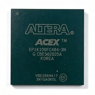
XC6SLX75T-2FG484I - 74K Spartan-6 LXT FPGA | AMD
MPN: XC6SLX75T-2FG484I ✗ 停產XC6SLX75T-2FG484I 概覽
A field-programmable gate array, or FPGA, is a semiconductor whose digital logic, memory, and I/O behavior are configured after manufacture. An FPGA belongs to the programmable-logic hierarchy and combines parallel programmable logic blocks with configurable input/output resources. This integration allows one physical device to implement control logic, signal processing, interface bridging, and embedded system functions without relying on a large collection of fixed-function logic ICs.
The Spartan-6 LX device family combines substantial programmable logic capacity with a high number of user I/Os. In the XC6SLX75T-2FG484I, 268 I/Os support communication with external processors, memory, converters, sensors, and industrial peripherals. The -2 performance grade and 667 MHz stated operating speed place the device in the Spartan-6 LX performance range, while the industrial-temperature suffix supports equipment designed for extended commercial and industrial operating environments.
The 484-ball FBGA package uses a 1 mm pitch and provides a compact, high-pin-count surface-mount footprint. Its 23 x 23 mm body makes it appropriate for dense control boards, but the fine ball pitch requires careful PCB layout, manufacturing control, inspection, and connector or test-point planning. The LXT designation also identifies this as a Spartan-6 member intended for designs requiring more logic resources and I/O capacity than smaller LX variants.
Typical uses include industrial automation, data acquisition, motion control, communications gateways, embedded instrumentation, and general-purpose digital signal processing. Its combination of 74,637 logic elements, 5,831 configurable logic blocks, and 268 I/Os is particularly useful when several parallel control paths, high-speed interfaces, and protocol conversion functions must share one programmable device.
PCB design should follow the AMD Spartan-6 package pinout files for every ball assignment and keep sensitive interfaces away from noisy power and switching paths. Decoupling, clock routing, configuration handling, bank voltage planning, and thermal performance require careful implementation before the FPGA is released for production.
This page organizes the principal device characteristics, practical application guidance, verified package details, and compatible Spartan-6 orderable variants into a focused engineering reference for design evaluation and component sourcing.
直接替換替代品,適用於 XC6SLX75T-2FG484I — 相同封裝,腳位對腳位相容。需重新設計 PCB 的不同封裝零件不列入。
此系列的變體
與下列產品可直接替換的同系列型號: XC6SLX75T-2FG484I (相同外形與佔位) — 差異在於 Ball Pitch, FPGA Family, Logic Elements, Mounting Type, Package Dimensions.
XC6SLX75T-2FGG484I
✅ 直接替換📋 參考替代品(不在目錄中)
XC6SLX75-2FG484I
✅ 直接替換聯絡詢價
查看資料表 →XC6SLX75T-3FGG484I
✅ 直接替換📋 參考替代品(不在目錄中)
XC6SLX75T-2CSG484I
✅ 直接替換📋 參考替代品(不在目錄中)
XC6SLX75-2FGG484I
✅ 直接替換聯絡詢價
查看資料表 →XC6SLX75T-2FG484I 最大額定值與電氣特性
| FPGA Family | Spartan-6 LXT |
| Configurable Logic Blocks | 5,831 CLBs |
| Logic Elements | 74,637 logic elements |
| Stated Operating Speed | 667 MHz |
| User I/O Count | 268 I/Os |
| Package Type | 484-ball FBGA |
| Package Dimensions | 23 x 23 mm |
| Ball Pitch | 1.0 mm |
| Terminal Count | 484 balls |
| Technology | CMOS |
| 安裝類型 | Surface-mount FBGA |
| Temperature Grade | Industrial |
| Performance Grade | -2 grade |
| Programmable Logic Type | FPGA |
| Package Body Size | 23 x 23 mm |
XC6SLX75T-2FG484I 23 x 23 mm 腳位配置指南
XC6SLX75T-2FG484I(23 x 23 mm 封裝)的腳位配置。 此數位 IC 包含 GPIO、通訊介面(UART、SPI、I2C)與電源腳位。替代腳位功能與配置選項請參閱製造商資料表。對嵌入式系統設計與 PCB 佈局至關重要。

無詳細腳位定義資料: XC6SLX75T-2FG484I.
請參閱 資料表 以查看完整腳位配置。
典型應用
XC6SLX75T-2FG484I 適用於 6 應用s: Industrial Automation and PLC Control, Data Acquisition and Instrumentation, Communications Gateway and Protocol Conversion, Embedded Signal Processing, Motor Control and Power-System Management, Aerospace and Defense Test Equipment.
Industrial Automation and PLC Control
The XC6SLX75T-2FG484I fits industrial controllers that coordinate motion, interlocks, actuators, sensors, and communications in parallel. Its 74,637 logic elements and 5,831 configurable logic blocks provide substantial capacity for state machines, timing logic, protocol conversion, and diagnostic logic, while 268 I/Os provide substantial connectivity to field-level circuits. The industrial-temperature order code is suitable for product platforms designed around extended industrial environments. Designers should assign I/O standards by bank, protect externally accessible signals, and isolate noisy relays or motor-drive stages from precision logic where practical.
推薦
Data Acquisition and Instrumentation
The XC6SLX75T-2FG484I is appropriate for parallel data-acquisition systems that must combine sensor conditioning, digital filtering, calibration tables, and a communications interface. Its 74,637 logic elements and 5,831 configurable logic blocks can support multiple processing pipelines concurrently, while 268 I/Os allow the device to interface with ADC data buses, status lines, clocks, and control signals. The stated 667 MHz operating speed supports timing-intensive digital functions. Board design should use controlled clock distribution, provide local decoupling for every supply group, and keep analog and digital grounding strategies consistent with the selected analog front end.
推薦
Communications Gateway and Protocol Conversion
The XC6SLX75T-2FG484I can serve in gateways that translate between serial, parallel, memory-mapped, and packet-oriented interfaces. Its 5,831 configurable logic blocks and 74,637 logic elements are well suited to concurrent buffering, framing, checksum, routing, and flow-control functions. With 268 I/Os, the device can support multiple external buses and control channels without relying on a large fixed-function chipset. Engineers should define clock-domain boundaries, constrain high-speed interfaces, and budget memory or external storage resources early because protocol conversion can consume logic and bandwidth faster than simple combinational control.
推薦
Embedded Signal Processing
The XC6SLX75T-2FG484I supports parallel filtering, correlation, modulation, waveform generation, and fixed-point signal-processing pipelines. Its 74,637 logic elements provide more implementation headroom than a small control FPGA, while the stated 667 MHz operating speed supports pipelined processing at useful clock rates. The 268 I/Os can connect the processor to parallel ADC or DAC data buses, memory, synchronization signals, and external peripherals. For reliable results, use synchronous design practices, pipeline arithmetic stages, apply appropriate clock constraints, and verify timing against all supported clock and configuration conditions.
推薦
Motor Control and Power-System Management
The XC6SLX75T-2FG484I can coordinate control sequencing, fault detection, pulse generation, and supervisory logic in motor-drive or power-conversion systems. Its extensive logic capacity allows current control, position tracking, protection state machines, and communications logic to coexist, while 268 I/Os simplify connection to gate drivers, position sensors, measurement systems, and safety-related discrete logic. The FPGA should remain separated from high-dv/dt power stages through appropriate isolation, filtering, and grounding. Production designs must also review the exact device temperature limits, operating voltages, transient behavior, and functional-safety requirements.
推薦
Aerospace and Defense Test Equipment
The XC6SLX75T-2FG484I can implement compact test and simulation systems when the surrounding equipment requires deterministic parallel logic, extensive interface connectivity, and programmable functionality. Potential uses include automated test equipment, avionics interface simulators, fault-injection systems, and programmable signal-generation platforms. The device's 74,637 logic elements and 268 I/Os allow one FPGA to coordinate acquisition, sequencing, and external communication. Because program-specific aerospace and defense requirements may exceed ordinary industrial specifications, engineers should confirm the exact ordering code, radiation, temperature, traceability, and qualification requirements before using the part in a safety-critical or export-controlled system.
推薦
推薦產品摘要
工程參考資料,適用於 XC6SLX75T-2FG484I — 比較、設計指引及合規資訊。
選型指南
與替代品比較
| 參數 | 本產品 | XC6SLX75T-2FGG484I | XC6SLX75-2FG484I | XC6SLX75T-3FGG484I | XC6SLX75T-2CSG484I | XC6SLX75-2FGG484I |
|---|---|---|---|---|---|---|
| Brand | AMD | AMD | AMD | AMD | AMD | AMD |
| Package | FBGA-484 (23 x 23 mm) | FBGA-484 (23 x 23 mm) - same package family | FBGA-484 (23 x 23 mm) - same package family | FBGA-484 (23 x 23 mm) - same package family | FBGA-484 (23 x 23 mm) - same package family | FBGA-484 (23 x 23 mm) - same package family |
| FPGA Family | Spartan-6 LXT | Spartan-6 LXT | Spartan-6 LXT | Spartan-6 LXT | Spartan-6 LXT | Spartan-6 LXT |
| Logic Elements | 74,637 | 74,637 | 74,637 | 74,637 | 74,637 | 74,637 |
| Configurable Logic Blocks | 5,831 CLBs | 5,831 CLBs | 5,831 CLBs | 5,831 CLBs | 5,831 CLBs | 5,831 CLBs |
| Ball Pitch | 1.0 mm | 1.0 mm | 1.0 mm | 1.0 mm | 1.0 mm | 1.0 mm |
| Performance Suffix | -2 | -2 | -2 | -3 | -2 | -2 |
主要差異化特點
- Exact 74,637-logic-element configuration (對比XC6SLX75T-3FGG484I)
- Closest documented package-code option (對比XC6SLX75T-2FGG484I)
- No logic-capacity penalty in the listed alternatives (對比XC6SLX75-2FGG484I)
設計說明
Treat the 484-ball FBGA as a fine-pitch assembly requiring a controlled PCB footprint and manufacturing process. Assign signals directly from the AMD package-device pinout file, preserve the exposed thermal and power-distribution structures required by the package documentation, and verify solder-mask, paste, and inspection capabilities at 1 mm pitch. Avoid constructing the footprint from visual ball spacing alone because package-specific mechanical tolerances and markings affect assembly.
Plan the complete power tree before routing high-speed interfaces. The device's 484-ball package provides many connections, but each supply domain still requires adequate decoupling and distribution. Place bulk and high-frequency decoupling capacitors close to their associated supply and ground balls, follow the manufacturer guidance for each rail, and confirm voltage-bank compatibility before assigning an I/O standard. Configuration voltage, auxiliary voltage, and normal operating supplies must remain within their specified limits.
Reserve a clear configuration and startup strategy that matches the complete device order code. Use dedicated clock-capable pins for system clocks where required, avoid routing sensitive clock or differential pairs through noisy power-stage areas, and apply source-synchronous or other appropriate PCB constraints for high-speed interfaces. Because the device has 268 I/Os, assign board functions and voltage standards during schematic capture rather than after PCB routing begins.
Do not interchange the target XC6SLX75T-2FG484I with similarly named 484-ball Spartan-6 order codes solely because their logic capacity matches. Verify the complete MPN, temperature suffix, performance grade, package code, and applicable AMD pinout file. A suffix change can alter ordering qualification or documentation without changing the broad 74,637-logic-element device family, making procurement and design traceability essential.
合規資訊
No explicit RoHS, REACH, AEC-Q100, lead-free, halogen-free, or conflict-minerals statement was established for this exact order code.