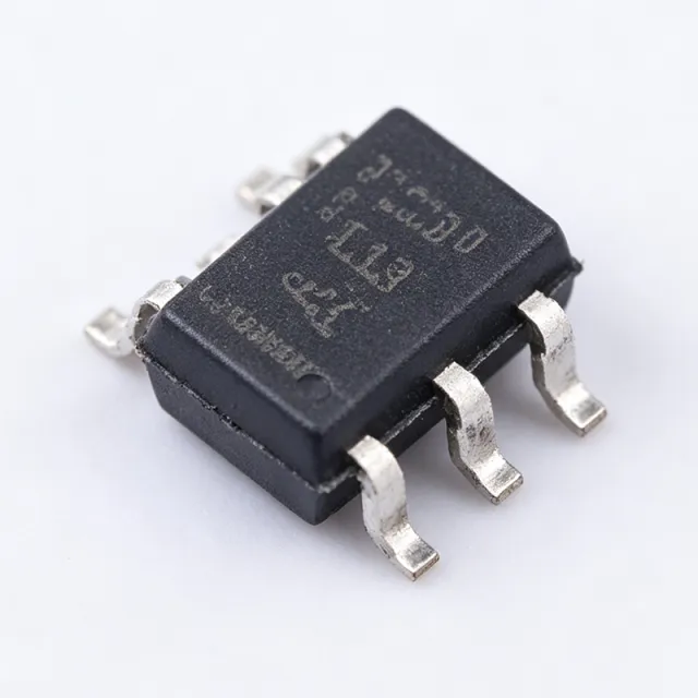
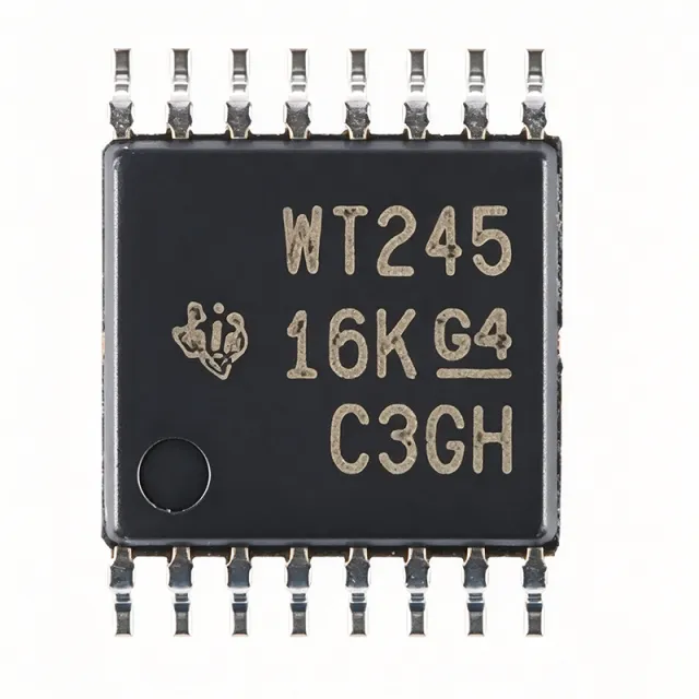
SN74AHC1G08DBV3
SN74AHC1G08DBV3 - 1-Ch 2-Input AND Gate, 2-5.5V | TI
The Texas Instruments SN74AHC1G08DBV3 is a single-channel, 2-input positive-AND gate from the AHC (Advanced High-Speed CMOS) logic family, housed in a 5-pin SOT-23 (DBV) package. It operates from a 2 V to 5.5 V supply, supports propagation delay of 9 ns maximum at 5 V (per TI's product page), and provides ±8 mA output drive at 5 V for driving moderate loads. The device performs the Boolean function Y = A · B in positive logic, making it a fundamental building block for digital decision-making and signal gating.
An AND gate is a basic combinational logic gate that produces a HIGH output only when all of its inputs are HIGH. Logic gates are the fundamental building blocks of digital integrated circuits, sitting at the lowest level of the digital design hierarchy: logic gate -> combinational logic -> sequential logic -> microcontroller / ASIC. The AHC family is a higher-speed, lower-power evolution of the classic HC (High-Speed CMOS) family, designed for low static power consumption while delivering faster switching than HC and lower switching noise than TTL.
Key features include a wide 2 V to 5.5 V operating range, ±8 mA balanced output drive at 5 V, 10 µA maximum quiescent supply current (Icc), and a Schmitt-trigger action on the inputs that makes the device tolerant of slowly rising edges. The SOT-23-5 footprint (DBV) is one of the industry's smallest logic-gate packages, enabling high-density board layouts in space-constrained designs. The device is also characterized for operation over the -55 °C to +125 °C free-air temperature range, suitable for industrial and harsh-environment applications.
Internally, the SN74AHC1G08 uses a standard CMOS push-pull output stage with a buffered input. The Schmitt-trigger input hysteresis typically exceeds 1 V at 5 V, which improves noise immunity in environments with slow or noisy input edges. The wide Vcc range allows the part to translate logic levels between 3.3 V and 5 V domains without external level shifters, useful when interfacing microcontrollers, sensors, and older 5 V peripherals.
Typical applications include power-rail sequencing and control logic in portable and battery-powered devices, enabling logic and control in industrial sensor interfaces, level shifting between 3.3 V and 5 V rails, general-purpose glue logic in microcontroller-based embedded designs, and signal gating in test and measurement equipment. The wide supply range and small package make it a versatile companion to virtually any digital subsystem.
When designing with this device, place a 0.1 µF decoupling capacitor as close as possible to the Vcc pin and minimize input trace lengths to avoid noise-induced glitches. Because this is a non-inverting AND function, be aware that it cannot be used as a NAND; if inverted output is required, cascade with an inverter such as SN74AHC1G04 in the same SOT-23-5 package.
This page synthesizes distributor pricing, drop-in same-package alternatives, and design guidance not always present in the manufacturer datasheet, providing actionable engineering reference for selection, replacement, and layout.
USD $0.25
有现货