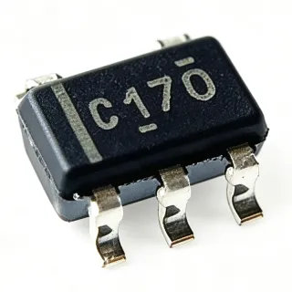
SN74AHC1G08DBV3 - 1-Ch 2-Input AND Gate, 2-5.5V | TI
料号: SN74AHC1G08DBV3 ✓ 量产中| 数量 | 单价 | 小计 |
|---|---|---|
| 1 | $0.53 | $0.53 |
| 10 | $0.46 | $4.60 |
| 100 | $0.38 | $38.00 |
| 500 | $0.31 | $155.00 |
| 1,000 | $0.25 | $250.00 |
SN74AHC1G08DBV3 概述
An AND gate is a basic combinational logic gate that produces a HIGH output only when all of its inputs are HIGH. Logic gates are the fundamental building blocks of digital integrated circuits, sitting at the lowest level of the digital design hierarchy: logic gate -> combinational logic -> sequential logic -> microcontroller / ASIC. The AHC family is a higher-speed, lower-power evolution of the classic HC (High-Speed CMOS) family, designed for low static power consumption while delivering faster switching than HC and lower switching noise than TTL.
Key features include a wide 2 V to 5.5 V operating range, ±8 mA balanced output drive at 5 V, 10 µA maximum quiescent supply current (Icc), and a Schmitt-trigger action on the inputs that makes the device tolerant of slowly rising edges. The SOT-23-5 footprint (DBV) is one of the industry's smallest logic-gate packages, enabling high-density board layouts in space-constrained designs. The device is also characterized for operation over the -55 °C to +125 °C free-air temperature range, suitable for industrial and harsh-environment applications.
Internally, the SN74AHC1G08 uses a standard CMOS push-pull output stage with a buffered input. The Schmitt-trigger input hysteresis typically exceeds 1 V at 5 V, which improves noise immunity in environments with slow or noisy input edges. The wide Vcc range allows the part to translate logic levels between 3.3 V and 5 V domains without external level shifters, useful when interfacing microcontrollers, sensors, and older 5 V peripherals.
Typical applications include power-rail sequencing and control logic in portable and battery-powered devices, enabling logic and control in industrial sensor interfaces, level shifting between 3.3 V and 5 V rails, general-purpose glue logic in microcontroller-based embedded designs, and signal gating in test and measurement equipment. The wide supply range and small package make it a versatile companion to virtually any digital subsystem.
When designing with this device, place a 0.1 µF decoupling capacitor as close as possible to the Vcc pin and minimize input trace lengths to avoid noise-induced glitches. Because this is a non-inverting AND function, be aware that it cannot be used as a NAND; if inverted output is required, cascade with an inverter such as SN74AHC1G04 in the same SOT-23-5 package.
This page synthesizes distributor pricing, drop-in same-package alternatives, and design guidance not always present in the manufacturer datasheet, providing actionable engineering reference for selection, replacement, and layout.
直接替换替代料: SN74AHC1G08DBV3 ——相同封装,引脚兼容。需要 PCB 改动的不同封装料号已排除。
快速对比工具——选择替代料号进行并排对比:
SN74AHC1G08DBVR
✅ 直接替换📋 参考替代料(不在目录中)
SN74AHC1G08DBVT
✅ 直接替换📋 参考替代料(不在目录中)
SN74AHCT1G08DBVR
✅ 直接替换📋 参考替代料(不在目录中)
SN74AHC1G08DBV3G4
✅ 直接替换 ⚠️ 规格未核验📋 参考替代料(不在目录中)
74AHC1G08GW
✅ 直接替换📋 参考替代料(不在目录中)
SN74AHC1G08DBV3 最大额定值与电气特性
| Manufacturer | Texas Instruments |
| Logic Type | AND Gate |
| Number of Channels | 1 |
| Number of Inputs per Channel | 2 |
| Logic Function | Y = A · B (positive-AND) |
| Supply Voltage (Vcc) | 2 V to 5.5 V |
| Propagation Delay (tpd) | 9 ns max at 5 V (per TI product page) |
| Output Drive (IOL / IOH) | ±8 mA at 5 V |
| Quiescent Supply Current (Icc) | 10 µA maximum |
| Input Type | Schmitt-Trigger |
| 工作温度范围 | -55 °C to +125 °C |
| 封装 | SOT-23-5 (DBV) |
| 安装类型 | Surface Mount |
| MSL 等级 | Level 1 (per TI datasheet) |
| RoHS 状态 | Compliant (Lead-free, Pb-free) |
SN74AHC1G08DBV3 引脚配置
| 引脚 1 | 1A — Data input A |
| 引脚 2 | GND — Ground |
| 引脚 3 | 2A — Data input B |
| 引脚 4 | Y — AND output (Y = A · B) |
| 引脚 5 | Vcc — Supply voltage (2 V to 5.5 V) |
典型应用
SN74AHC1G08DBV3 适用于 6 应用s: Power-Rail Sequencing and Control Logic, Industrial Sensor Interface and Control Logic, 3.3 V to 5 V Logic-Level Translation, General-Purpose Glue Logic in Embedded Designs, Test and Measurement Equipment Signal Gating, Battery-Powered Portable and Wearable Devices.
Power-Rail Sequencing and Control Logic
The SN74AHC1G08DBV3's wide 2 V to 5.5 V supply and ±8 mA output drive at 5 V make it well suited for sequencing multiple power rails in portable and embedded systems. With 9 ns max tpd at 5 V (per TI product page) and 10 µA maximum quiescent current, it contributes negligible quiescent drain while responding fast enough to satisfy most sequencing timing budgets. A common topology combines a power-good signal and a soft-start done signal into the two AND inputs; the Y output then drives the enable pin of a downstream DC-DC converter. The SOT-23-5 footprint fits adjacent to almost any controller IC without area penalties. Unlike discrete BJT-RC timing circuits, this gate-based sequencer has well-defined logic thresholds and consistent behavior over temperature, which is critical for production test repeatability.
推荐
Industrial Sensor Interface and Control Logic
Industrial sensors often produce digital signals that must be gated, qualified, or combined before being fed to a microcontroller or PLC input. The SN74AHC1G08DBV3 handles two such signals and presents a clean logic-low or logic-high output with ±8 mA of drive at 5 V. Its 2 V to 5.5 V supply tolerance allows it to ride through transients on poorly regulated 5 V industrial rails, and the -55 °C to +125 °C operating range handles outdoor and factory-floor temperatures. Inputs are Schmitt-trigger, providing noise immunity in electrically noisy environments such as motor-control cabinets where the gate sits near power devices. The SOT-23-5 footprint eases integration onto small sensor break-out PCAs. Compared with a discrete BJT AND circuit, this part delivers predictable VIH/VIL thresholds and symmetric output drive, improving design margin.
推荐
3.3 V to 5 V Logic-Level Translation
Level translation between 3.3 V and 5 V domains is one of the most common uses of the SN74AHC1G08DBV3. With its 2 V to 5.5 V Vcc range and TTL-compatible thresholds, the gate can be powered from a 5 V rail while accepting 3.3 V CMOS inputs at VIH of 2.0 V minimum at 5 V Vcc. The output Y then swings full 0 V to 5 V for downstream 5 V logic, producing clean logic-level transitions without external pull-ups or level shifter ICs. Propagation delay of 9 ns at 5 V (per TI product page) is fast enough for I2C, SPI, GPIO, and other low-to-medium speed interfaces. The wide Vcc tolerance means the gate handles supply variations gracefully. Compared with a dedicated level-shifter IC, this AHC gate is cheaper, smaller, and simpler to place, although it does not provide the isolation of a true level-shifter.
推荐
General-Purpose Glue Logic in Embedded Designs
In microcontroller-based designs, the SN74AHC1G08DBV3 acts as classic glue logic, combining enable, chip-select, write-protect, or interrupt-acknowledge signals that the MCU pins cannot otherwise manage efficiently. The 1-channel, 2-input AND function performs the Boolean Y = A · B with positive logic, supporting common cases such as dual enable gating and qualified write strobes. With 2 V to 5.5 V Vcc it adapts to 1.8 V/3.3 V/5 V rails, and the SOT-23-5 footprint consumes minimal board area near the MCU. The Schmitt-trigger inputs clean up slow or bouncing signals from mechanical switches or long cables, making it useful as a debounce combinator in HMI modules. Compared with implementing the same logic in software, this hardware gate provides deterministic timing independent of interrupt latency.
推荐
Test and Measurement Equipment Signal Gating
In test and measurement instruments, the SN74AHC1G08DBV3 is used to gate test signals, qualify calibration pulses, and combine handshake signals between measurement modules. With 9 ns propagation delay at 5 V (per TI product page) and ±8 mA output drive, it preserves pulse integrity in sub-100 ns timing paths without distorting rising edges. The SOT-23-5 package fits inside dense measurement channel PCBs, and the -55 °C to +125 °C operating range ensures stable behavior in unheated instrument enclosures. Inputs feature Schmitt-trigger action, helping reject noise from relay switching and AC mains spurs. Compared with analog gating, this digital AND function does not introduce analog offsets or drift, simplifying calibration and traceability.
推荐
Battery-Powered Portable and Wearable Devices
In battery-powered devices, the SN74AHC1G08DBV3 contributes only 10 µA maximum quiescent current and operates down to 2 V, making it compatible with single-cell Li-ion or two-AA battery rails. Its AND function combines wake-up events, button-press qualification, or sensor-ready flags in low-power state machines. The SOT-23-5 footprint integrates adjacent to a power-management IC without area penalty, and the -55 °C to +125 °C operating range covers cold-weather wearable and outdoor use cases. Compared with discrete MOSFET AND logic, this IC provides well-defined thresholds and stable switching characteristics across the battery voltage range, improving system robustness as cells discharge.
推荐
推荐产品汇总
工程参考数据: SN74AHC1G08DBV3 ——对比、设计指导和合规信息。
选型指南
与替代料对比
| 参数 | 本产品 | SN74AHC1G08DBVR | SN74AHC1G08DBVT | SN74AHCT1G08DBVR | SN74AHC1G08DBV3G4 | 74AHC1G08GW |
|---|---|---|---|---|---|---|
| Brand | Texas Instruments | Texas Instruments | Texas Instruments | Texas Instruments | Texas Instruments | Nexperia |
| Package | SOT-23-5 (DBV) | SOT-23-5 (DBV) - same | SOT-23-5 (DBV) - same | SOT-23-5 (DBV) - same | SOT-23-5 (DBV) - same | SOT-23-5 (DBV-equivalent) - same outline |
| Logic Function | 1-ch 2-input AND | 1-ch 2-input AND | 1-ch 2-input AND | 1-ch 2-input AND (TTL inputs) | 1-ch 2-input AND | 1-ch 2-input AND |
| Supply Voltage (Vcc) | 2 V to 5.5 V | 2 V to 5.5 V | 2 V to 5.5 V | 4.5 V to 5.5 V | 2 V to 5.5 V | 2 V to 5.5 V |
| Propagation Delay (tpd) | 9 ns max at 5 V | 9 ns max at 5 V | 9 ns max at 5 V | 9 ns max at 5 V | 9 ns max at 5 V | ~10 ns max at 5 V (typical AHC) |
| Output Drive (IOL/IOH) | ±8 mA at 5 V | ±8 mA at 5 V | ±8 mA at 5 V | ±8 mA at 5 V | ±8 mA at 5 V | ±8 mA at 5 V |
| Input Type | Schmitt-Trigger CMOS | Schmitt-Trigger CMOS | Schmitt-Trigger CMOS | Schmitt-Trigger TTL-compatible | Schmitt-Trigger CMOS | Schmitt-Trigger CMOS |
| Operating Temperature | -55 °C to +125 °C | -55 °C to +125 °C | -55 °C to +125 °C | -55 °C to +125 °C | -55 °C to +125 °C | -40 °C to +125 °C (typical) |
关键差异点
- Wide 2 V to 5.5 V Vcc supports both 3.3 V and 5 V logic in a single part (对比 SN74AHCT1G08DBVR (4.5 V to 5.5 V only))
- Industry-standard SOT-23-5 footprint with broad second-source availability (对比 Nexperia 74AHC1G08GW)
- Schmitt-trigger inputs provide hysteresis for noise immunity (对比 SN74LVC1G08 (non-Schmitt input))
设计说明
Place a 0.1 µF ceramic decoupling capacitor as close as possible to the Vcc pin (Pin 5) and to the GND pin (Pin 2). For designs with multiple AHC gates sharing a rail, add a 1 µF to 10 µF bulk capacitor near the supply entry to the gate section. The SN74AHC1G08DBV3's quiescent current is only 10 µA maximum, but transient switching current can briefly exceed this and cause supply sag without adequate decoupling.
The SN74AHC1G08DBV3 is a non-inverting AND function (Y = A · B). It cannot be used as a NAND - if inverted output is required, pair with SN74AHC1G04DBV3 in the same SOT-23-5 package, or substitute SN74AHC1G00DBV3 NAND gate. Also note that the AHC family does not have TTL-compatible inputs at all Vcc levels; if your design needs 3.3 V TTL inputs to drive 5 V CMOS, choose SN74AHCT1G08DBVR instead, which has TTL-level thresholds across the 4.5 V to 5.5 V range.
Minimize trace length on inputs (Pins 1 and 3) to reduce noise pickup; long input traces on slow CMOS logic can couple noise and cause spurious output transitions. Keep ground return paths short and avoid routing signal traces under the part or near switching power inductors. The exposed thermal pad is not present on the SOT-23-5 - thermal management is not a concern at 10 µA quiescent and ±8 mA drive.
合规信息
RoHS-compliant Pb-free finish per TI product page. Logic gate not subject to AEC-Q100 automotive qualification in this generic-grade option; for automotive variants choose the SN74AHC1G08-Q1 family.