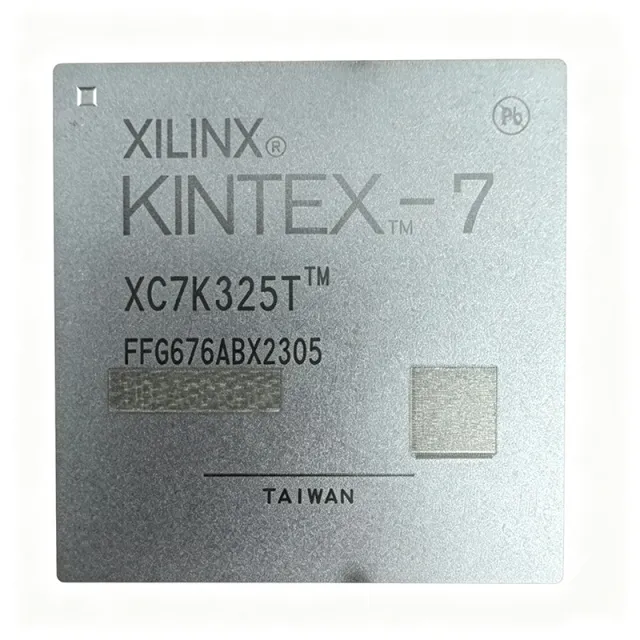
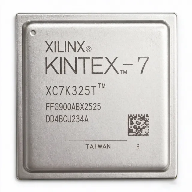
XC7K160T-2FF676I
XC7K160T-2FF676I - 162K Kintex-7 FPGA | AMD Xilinx
AMD Xilinx XC7K160T-2FF676I is a Kintex-7 field-programmable gate array with 162,240 logic cells, 250 user I/Os, a maximum clock frequency of 710 MHz, and a 676-ball FCBGA package. The -2 speed grade targets designs requiring a balance of performance, power consumption, and design flexibility across industrial, communications, instrumentation, and embedded processing systems.
A field-programmable gate array is a semiconductor whose digital logic can be configured after manufacture. An FPGA belongs to the programmable-logic hierarchy, combining configurable logic blocks, programmable I/O, block RAM, DSP arithmetic resources, clock-management circuits, and high-speed serial transceivers. This architecture allows parallel processing, hardware acceleration, protocol bridging, and deterministic control functions to be consolidated into one device rather than implemented across multiple fixed-function chips.
The XC7K160T belongs to the Kintex-7 family and provides 162,240 logic cells with a stated maximum operating frequency of 710 MHz. Its 250 I/Os support connection to external memory, high-speed interfaces, control signals, clocks, and data converters. The 676-ball FCBGA package also exposes the device's high-speed I/O and configuration resources, while its fine-pitch ball pitch makes careful PCB layout, thermal management, and assembly process control essential.
The -2 suffix identifies the device speed grade. Compared with a -1 part, the -2 grade provides a higher performance level; a -3 grade is faster still. Core-voltage information associated with this device lists an operating range of 970 mV to 1.03 V. Because Kintex-7 devices contain configurable power-management features, actual rail requirements and current depend on the selected logic, memory interfaces, transceivers, I/O standards, clocking, and utilization reported by the implementation tools.
Typical uses include industrial control, communications infrastructure, test and measurement, high-speed data acquisition, signal processing, network equipment, and embedded systems that benefit from parallel programmable logic. The large logic capacity supports parallel datapaths, protocol state machines, packet processing, and custom accelerator pipelines. Integrated block RAM and DSP resources can reduce reliance on external components when the design maps efficiently onto the FPGA architecture.
When laying out a board around this FCBGA device, follow the manufacturer pinout, power-plane, decoupling, and high-speed-interface guidance exactly. Provide continuous supply planes, place bypass capacitors at the relevant power balls, route clock and differential pairs with controlled impedance, and confirm the assembly process supports the package geometry. Check worst-case junction temperature, configured transceivers, I/O standards, and core utilization before approving the power budget.
This product record combines the exact manufacturer-family parameters, package information, speed-grade references, drop-in candidates, and engineering guidance needed to evaluate a board-level migration. It emphasizes where an alternate speed grade changes performance, where package suffixes require procurement review, and which design constraints remain unchanged when the FPGA itself is replaced.
询价
联系我们