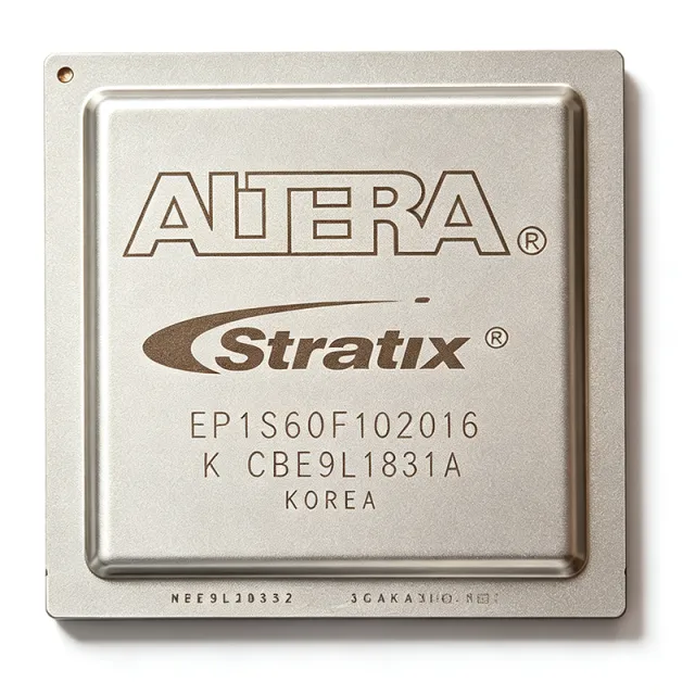
EP1S80F1020C7
EP1S80F1020C7 - Stratix 79,040 Logic Element FPGA | Intel (Altera)
The Intel (formerly Altera) EP1S80F1020C7 is a high-density Stratix Field Programmable Gate Array (FPGA) integrating 79,040 logic elements and 7,427,520 system gates in a 1020-ball FineLine BGA package (33 x 33 mm, 1 mm pitch) with 773 user I/O pins. Per the manufacturer datasheet, it operates from a 1.425 V to 1.575 V core supply and is rated for the commercial 0 C to 85 C temperature range, making it suitable for mainstream logic and DSP prototyping designs.
An FPGA (Field Programmable Gate Array) is a programmable logic device containing an array of configurable logic blocks (CLBs), programmable interconnect, and dedicated hard IP blocks such as block RAM, DSP multipliers, PLLs, and high-speed transceivers. Within the broader semiconductor taxonomy, FPGAs sit alongside CPUs, GPUs, and ASICs as a programmable hardware platform, and are commonly categorized under logic ICs / programmable logic. The Stratix family was Altera's first-generation high-performance FPGA family, later succeeded by Stratix II, III, IV, and V. The EP1S80 sits at the top of the Stratix density ladder, providing 7,427,520 typical gates which is the maximum logic density available in the family.
Key specifications include 79,040 logic elements organized into 7,904 logic array blocks (LABs), 773 user I/O pins supporting multiple I/O standards (LVDS, LVTTL, LVCMOS, SSTL, HSTL, PCI, PCI-X), embedded TriMatrix memory blocks, dedicated DSP blocks for high-speed multiplication and accumulation, up to 12 PLLs for clock management, and configuration via passive serial (PS), fast passive parallel (FPP), or JTAG modes. The 1020-ball FBGA package uses a 1 mm pitch and measures 33 x 33 mm on the PCB, requiring multi-layer PCB design with controlled-impedance traces and matched-length routing for the high-speed LVDS pairs.
Typical applications include high-throughput digital signal processing (software-defined radio, radar, video processing), telecom line cards and protocol bridging, high-speed serial protocol bridging, ASIC prototyping and emulation, test and measurement equipment, and military/aerospace signal processing platforms where large logic density and embedded DSP resources are required. The integrated PLLs and dedicated clock networks also make it suitable as a glue-logic aggregation device between multiple processors and peripherals.
When designing with the EP1S80F1020C7, attention must be paid to power architecture: a multi-rail supply (VCCINT, VCCIO banks, VCCPD, VCCA_PLL, VCCBAT) is required, with multiple decoupling capacitors placed close to the BGA balls. The Quartus II design suite (Altera/Intel) is the required toolchain for synthesis, place-and-route, and bitstream generation. The 33 x 33 mm FBGA package requires a high-layer-count PCB (typically 8 to 12 layers) with via-in-pad or dog-bone fanout for reliable BGA assembly.
This page synthesizes distributor pricing, drop-in Stratix family alternatives, and practical design notes (BGA fanout, multi-rail decoupling, configuration mode selection) not consolidated in the manufacturer datasheet, helping engineers compare density, speed grade, and I/O count when selecting a Stratix device.
询价
联系我们