MOSFET
产品(1294)

IPB120P04P404ATMA2 - 40V P-Channel 120A OptiMOS MOSFET | Infineon
The Infineon IPB120P04P404ATMA2 is a P-channel power MOSFET from Infineon's OptiMOS-P2 family, rated at 40V drain-source breakdown and 120A continuous drain current (Tc) in a PG-TO263-3-2 (D2PAK) surface-mount package. It delivers a typical on-state resistance of 3.8 mOhm at VGS=-10V and ID=-100A, total gate charge of 205 nC at VGS=-10V, and an input/output capacitance of 14,790 pF at 25V. Maximum power dissipation is 136W (Tc) and 1.7W (TA, with appropriate PCB footprint). A P-channel MOSFET is a type of field-effect transistor in which the conductive channel is formed by holes rather than electrons. P-channel devices simplify high-side load switching because the source is tied to the positive rail and a gate voltage pulled toward ground turns the device on, eliminating the charge pump or bootstrap circuitry required by N-channel high-side drivers. P-channel MOSFETs occupy the power MOSFET -> discrete semiconductor -> power management hierarchy, and they are the traditional choice for load switching, reverse-battery protection, and high-side ORing in 12V/24V automotive and industrial systems. Key features of this part include the OptiMOS-P2 trench process which minimizes FOM (RDS(on) x Qg), a logic-level compatible -10V/-20V gate drive range, low thermal resistance junction-to-case (RthJC < 1 C/W typical), and avalanche-rated single-pulse robustness. The 3.8 mOhm RDS(on) figure reduces conduction loss versus prior-generation P-channel parts, while the -20V VGS(max) rating provides headroom against inductive transients and gate over-drive. The PG-TO263-3-2 package is footprint-compatible with industry-standard D2PAK, allowing direct replacement or upgrade in existing layouts. Architecturally, the device uses Infineon's trench MOSFET cell technology to achieve a low figure-of-merit, with a body diode optimized for third-quadrant conduction. The result is a part that competes effectively with both discrete P-channel MOSFETs and integrated high-side switches in efficiency-critical designs. Performance is optimized for switching frequencies in the 50 kHz to 500 kHz range commonly used in synchronous buck, buck-boost, and motor-drive topologies. Typical applications include high-side load switching in automotive ECUs, reverse-polarity protection in 12V/24V industrial battery systems, DC-DC converter high-side switches, motor drive H-bridges, hot-swap controllers, ORing FETs in redundant power architectures, and battery management systems. The part is widely used in power tools, e-bike controllers, USB-PD source controllers, and telecom DC distribution. When designing with this part, ensure VGS never exceeds +/-20V, account for self-heating at high continuous loads, and use Kelvin-source sensing if available. The exposed tab (tab = drain) must be soldered to a copper pour of at least 1 square inch to achieve rated power dissipation. This page synthesizes distributor pricing, drop-in alternatives, and practical design notes not found in the manufacturer datasheet.

IPB120P04P4L03ATMA2 - 40V P-Channel MOSFET, 120A, D2PAK | Infineon
The Infineon IPB120P04P4L03ATMA2 is a P-channel OptiMOS-P2 power MOSFET rated at 40 V VDS, 120 A continuous drain current (Tc), and 136 W power dissipation (Tc), housed in a surface-mount PG-TO263-3-2 (D2PAK) package with an on-resistance of approximately 3.1 mΩ (per Infineon's product summary). It belongs to Infineon's OptiMOS-P2 family, which targets high-current, low-loss P-channel switching in 12 V/24 V automotive and industrial buses. What is a P-channel MOSFET? A P-channel metal-oxide-semiconductor field-effect transistor (P-channel MOSFET) is a type of power transistor that conducts when its gate is pulled below the source potential. In the system taxonomy, a P-channel MOSFET sits under: MOSFET -> power transistor -> discrete semiconductor -> power management component. P-channel devices are commonly used for high-side switching because they can be placed directly on the positive rail without a charge pump in some topologies, although N-channel MOSFETs generally offer lower RDS(on) for the same silicon area. Key features include a 40 V drain-source breakdown (V(BR)DSS), a continuous drain current rating of 120 A at case temperature 25 °C, pulsed current capability for motor inrush, an industry-standard D2PAK footprint, and an operating junction temperature range up to 175 °C. The '03' designator indicates an OptiMOS-P2 generation with optimized body diode reverse recovery and Qrr for synchronous-rectification-friendly behavior. Typical applications include high-side motor bridges in 12 V/24 V automotive systems (e.g., window lift, seat control, HVAC blowers), electronic fuse (e-fuse) and load switch circuits, reverse-battery protection blocks, DC-DC converter high-side switches, and battery management isolation FETs. The P-channel polarity eliminates the bootstrap supply needed for N-channel high-side drivers, simplifying gate drive. When designing with this device, gate drive must swing below the source rail to fully enhance the channel. A 10 V gate drive is typical, and TVS protection on the gate is recommended in motor applications where dv/dt and back-EMF transients couple into the gate loop.

IPB17N25S3100ATMA1 - 250V 17A N-Channel MOSFET | Infineon
The Infineon IPB17N25S3100ATMA1 is a 250 V N-channel enhancement-mode power MOSFET in a PG-TO263-3-2 (D2PAK) surface-mount package, qualified to AEC-Q101 for automotive use. It features a continuous drain current of 17 A at Tc, a maximum drain-source on-resistance of 100 mOhm at VGS = 10 V, and a pulsed current capability of 64 A for transient loads. A power MOSFET (Metal-Oxide-Semiconductor Field-Effect Transistor) is a voltage-controlled semiconductor switch used in power conversion and motor-drive applications. MOSFETs sit within the broader hierarchy of discrete semiconductors (transistors), and as an N-channel enhancement-mode part, IPB17N25S3100ATMA1 turns on when a positive gate-source voltage is applied. It belongs to Infineon's OptiMOS family, where low RDS(on) per silicon area reduces conduction losses in high-current switching topologies. Key specifications include a drain-source voltage (VDS) of 250 V, gate-source voltage (VGS) of +/-20 V, total gate charge (Qg) of 19 nC at VGS = 10 V, input capacitance (Ciss) of 1.5 nF, and output capacitance (Coss) of 23 pF. The threshold voltage (VGS(th)) is 4 V, with avalanche-rated ruggedness (100% avalanche tested) and a maximum power dissipation of 107 W at Tc = 25 C. The device uses Infineon's trench-technology cell structure to achieve the 19.3 mOhm typical RDS(on) figure cited in manufacturer collateral, balancing low conduction loss with manageable switching loss for hard-switched converters. The D2PAK package offers a low thermal resistance path suitable for tab-screw mounting or large PCB copper areas. Typical applications include automotive DC-DC converters, 48 V mild-hybrid systems, motor-drive inverter stages, solenoid drivers, and industrial switched-mode power supplies. The 250 V rating also suits telecom brick converters and photovoltaic micro-inverter front-ends. When designing with this part, choose gate-drive voltage of 10 V for full enhancement and minimize loop inductance between drain and source to control switching transients. The tab is electrically connected to the drain; mounting isolation must be considered for heatsink-attached designs. This page synthesizes distributor pricing, drop-in alternatives, and practical thermal and PCB layout notes not found in the manufacturer datasheet alone, giving engineers a one-stop reference for selection and sourcing.
IPB180P04P4L02ATMA2 - 40V P-Channel 180A OptiMOS-P2 MOSFET | Infineon
The Infineon IPB180P04P4L02ATMA2 is a 40 V P-Channel OptiMOS-P2 power MOSFET rated for 180 A continuous drain current at Tc and 150 W power dissipation, housed in a surface-mount PG-TO263-7-3 (D2PAK-6) package. It is a member of Infineon's OptiMOS-P2 family, the second-generation automotive-grade P-channel platform targeting high-current switching at low on-state loss. The part is qualified to AEC-Q101 for automotive use. A P-Channel MOSFET is a voltage-controlled power transistor whose conduction channel is formed by negative charge carriers (holes) between source and drain. Compared with N-channel MOSFETs, P-channel parts simplify high-side switching by eliminating the charge pump or bootstrap circuit normally required to drive an N-channel high-side FET, which reduces BOM cost and PCB area. P-channel MOSFETs sit in the hierarchy: P-channel MOSFET -> MOSFET -> power transistor -> discrete semiconductor. The OptiMOS-P2 generation specifically targets the highest figure of merit for low-voltage (<=40 V) high-current switching applications. Key specifications include a maximum drain-source voltage VDS of 40 V, continuous drain current ID of 180 A at Tc, pulsed avalanche current handling that supports motor-drive transients, and an extremely low typical on-state resistance RDS(on) of 2.4 mOhm at VGS = 10 V (according to Infineon's product summary page). The P-channel polarity and -10 V gate drive are standard for high-side load switching. PG-TO263-7-3 (D2PAK-6) is a 7-pin surface-mount package with a large metal tab that doubles as the drain connection and provides a low-thermal-resistance path to the PCB. The OptiMOS-P2 trench technology uses an advanced cell pitch and a P-epi drain structure to minimize the RDS(on) x Qg figure of merit. The die is optimized for high peak current handling and low conduction loss, and is screened to Infineon's automotive-grade reliability flow. The -02 suffix denotes a specific VGS(th) and RDS(on) bin within the OptiMOS-P2 family. Typical applications include high-side load switches in 12 V / 24 V automotive board nets, motor-bridge switches for small DC motors and pumps, reverse-battery protection FETs, and power-ORing switches in redundant supply architectures. The P-channel topology makes it particularly attractive as a high-side switch that is driven directly from a logic-level MCU without needing a level-shifter. When designing with this part, note that the source pin sits at the load (system voltage) side, so the tab/drain is the low-side (ground) terminal. Gate drive must reach at least 10 V below the source for full enhancement. For thermal management at 150 W PDC, copper-pour area under the tab should be sized to keep Tj below 175 C at worst-case continuous load. This page synthesizes distributor pricing, AEC-Q101 alternatives, and design considerations not consolidated in the manufacturer datasheet.

IPB200N25N3GATMA1 - 250V 64A OptiMOS 3 N-Ch MOSFET | Infineon
The Infineon IPB200N25N3GATMA1 is a 250 V, 64 A N-channel power MOSFET built on Infineon's OptiMOS 3 technology, housed in a surface-mount PG-TO263-3 (D2PAK) package. It combines a 250 V drain-source breakdown voltage, 64 A continuous drain current (at Tc), and an industry-leading R_DS(on) maximum of 20 mOhm for synchronous rectification and high-current DC-DC conversion. The die is qualified to 300 W power dissipation at case temperature, enabling dense power designs without paralleling. A power MOSFET is a voltage-controlled semiconductor switch used to efficiently route or modulate current between the drain and source terminals. N-channel MOSFETs such as the IPB200N25N3GATMA1 are the dominant building blocks of modern switched-mode power conversion, falling within the broader hierarchy of discrete semiconductors -> transistors -> MOSFETs -> power MOSFETs. OptiMOS 3 represents Infineon's third-generation trench MOSFET platform optimized for low figure-of-merit (R_DS(on) x Q_g), reducing both conduction and switching losses. Key features include a maximum R_DS(on) of 20 mOhm at V_GS = 10 V, an ultra-low gate charge Q_g, and a logic-level-friendly gate threshold that simplifies gate-drive design. The D2PAK (PG-TO263-3) surface-mount package delivers a low thermal resistance from junction to case, allowing the 300 W dissipation rating to be fully realized on FR-4 PCB with adequate copper area. The part is halogen-free and RoHS-compliant, fitting modern environmental regulations. The OptiMOS 3 process uses a deep-trench cell structure that simultaneously minimizes on-resistance and gate charge. This figure-of-merit balance is critical in high-frequency synchronous rectification, where every switching cycle accumulates losses proportional to Q_g. The 250 V rating also provides comfortable margin above 48 V telecom and 60 V industrial bus rails, supporting 80 V transient tolerance commonly required in those systems. Typical applications include synchronous rectification in 48 V telecom DC-DC converters, primary-side switches in uninterruptible power supplies (UPS), DC motor drive inverters, and high-current point-of-load converters. The 250 V drain rating also makes it suitable for 120 V AC rectified rails, solar micro-inverters, and industrial SMPS where a single high-current switch replaces older-generation planar MOSFETs. When designing with this part, prioritize PCB layout for low source-inductance and adequate copper area under the D2PAK tab for thermal dissipation. Use a gate driver capable of sourcing/sinking at least 1 A peak to fully exploit the fast switching edge, and ensure the gate-source voltage remains within +/-20 V to prevent oxide failure. This page synthesizes distributor pricing, drop-in alternatives in the same D2PAK footprint, and practical design notes not found in the manufacturer datasheet alone.

IPB35N10S3L26ATMA1 - 100V 35A N-Ch OptiMOS-T MOSFET | Infineon
The Infineon IPB35N10S3L26ATMA1 is an N-channel OptiMOS-T power MOSFET rated at 100 V VDS and 35 A continuous drain current (at TC), housed in a surface-mount PG-TO263-3 (D2PAK-2) package with a maximum power dissipation of 71 W (TC). It delivers an ultra-low on-state resistance and is targeted at high-efficiency switching applications where automotive-grade reliability is required. An N-channel power MOSFET is a voltage-controlled semiconductor device in which a positive gate-source voltage creates an inversion layer that conducts current between drain and source. Within the broader taxonomy, this part belongs to power MOSFET -> discrete semiconductor -> power transistor, and specifically to Infineon's OptiMOS-T family which is tuned for low-voltage, high-current switching with optimized FOM (figure-of-merit) for both conduction and switching losses. Key features highlighted by the Verified Web Data include the 100 V drain-source voltage rating, 35 A continuous drain current capability, 71 W power dissipation, and a D2PAK-2 (PG-TO263-3) SMD footprint suitable for automated assembly. The OptiMOS-T process technology reduces gate charge and output capacitance, allowing faster switching transitions and reduced driver losses. The part also benefits from a low R_DS(on) (manufacturer page references 26.3 mΩ as a typical figure of merit) and an avalanche-rated body diode, which improves robustness in inductive load switching. Typical applications include DC-DC converters in 48 V automotive systems, motor drive half-bridges in industrial and e-mobility platforms, synchronous rectification in telecom and server power supplies, solenoid and relay drivers, and high-current load switching in battery management systems. The low thermal resistance of the D2PAK package enables direct PCB heatsinking through the exposed tab. When designing with this MOSFET, ensure adequate copper area on the PCB beneath the exposed pad to dissipate up to 71 W at elevated case temperatures, and select a gate driver capable of sourcing/sinking the appropriate Qg to achieve the desired switching frequency. AEC-Q101 automotive-grade reliability should be verified against the specific Infineon's datasheet revision for production designs.

IPB35N10S3L26ATMA2 - 100V 35A N-Ch OptiMOS MOSFET | Infineon
The Infineon IPB35N10S3L26ATMA2 is an N-channel power MOSFET built on Infineon's OptiMOS power-transistor technology, rated for 100 V drain-source voltage and 35 A continuous drain current (at Tc) in a surface-mount PG-TO263-3-2 (D2PAK) package with 71 W power dissipation (at Tc). The part belongs to the 75 V to 120 V OptiMOS family and features a typical R<sub>DS(on)</sub> of 26.3 mOhm optimized for low conduction loss. A MOSFET (Metal-Oxide-Semiconductor Field-Effect Transistor) is a voltage-controlled switching device that uses an insulated gate to modulate current flow between drain and source terminals. Power MOSFETs sit within the broader semiconductor taxonomy: transistor -> discrete semiconductor -> MOSFET -> N-channel power MOSFET. OptiMOS is Infineon's proprietary power-MOSFET process platform targeting low on-resistance, fast switching, and high efficiency in switched-mode power conversion. The IPB35N10S3L-26 specifically belongs to the automotive-grade OptiMOS family, delivering enhanced avalanche ruggedness and a 180 A pulsed current capability suited to harsh-environment switching. Key features include a logic-level-compatible gate threshold for direct microcontroller drive, low gate charge (Qg) for reduced driver losses, and an integrated body diode for inductive-load switching. The 100 V breakdown voltage provides ample margin for 48 V automotive and industrial bus architectures, while the 35 A continuous rating supports high-current load switches and motor-drive half-bridges. The OptiMOS process combines a trench-gate cell structure with optimized minority-carrier lifetime control, achieving a figure-of-merit (FOM = R<sub>DS(on)</sub> x Qg) that significantly improves switching efficiency over older planar MOSFET generations. The D2PAK (PG-TO263-3-2) package provides a low thermal-resistance path through its exposed tab, enabling direct PCB heatsinking. Typical applications include 48 V automotive systems, DC-DC converters, motor-drive H-bridges, solenoid drivers, and high-side load switches. The device is well suited to battery management, electric power steering, and braking system power stages where efficiency, robustness, and surface-mount manufacturability are required. When designing with the IPB35N10S3L26ATMA2, ensure the gate-drive voltage meets the threshold and plateau requirements; insufficient Vgs increases R<sub>DS(on)</sub> and conduction loss. For switching applications above 50 kHz, gate-drive loops must be minimized to control ringing and dv/dt-induced turn-on. This page synthesizes distributor pricing, drop-in alternatives, and practical design notes not found in the manufacturer datasheet alone.
IPB45N06S4L08ATMA3 - 60V 45A OptiMOS-T2 N-Channel MOSFET | Infineon
The Infineon IPB45N06S4L08ATMA3 is an N-channel enhancement-mode Power MOSFET from Infineon's OptiMOS-T2 family, rated for 60V VDS and continuous drain current of 45A (TC), housed in the surface-mount PG-TO263-3-2 (D2PAK) package with 71W power dissipation capability. Built on Infineon's mature OptiMOS-T2 trench technology, it targets automotive and industrial switching applications where both low conduction loss and high current handling are required. An N-channel MOSFET is a voltage-controlled semiconductor switch where a positive gate-source voltage creates an inversion layer that conducts current between drain and source. The OptiMOS-T2 family represents Infineon's mid-voltage (40V-300V) trench MOSFET product line within the broader power-MOSFET taxonomy: trench MOSFET -> power MOSFET -> discrete semiconductor -> semiconductor. Compared to older planar MOSFETs, trench technology achieves much lower on-resistance per unit silicon area, reducing conduction losses and shrinking die/package size. Key features include a maximum on-resistance of 7.9 mΩ (RDS(on) at VGS=10V), low switching and conduction losses for high thermal efficiency, AEC-Q101 automotive qualification, 100% avalanche-tested ruggedness, MSL1 moisture sensitivity rating up to 260°C peak reflow, and a 175°C maximum operating junction temperature. The part is also a Green Product, fully RoHS compliant, and ships on tape and reel for high-volume SMT assembly lines. The 7.9 mΩ RDS(on) figure translates directly into conduction loss: at 20A continuous load the device dissipates roughly P = I² x R = 20² x 0.0079 ≈ 3.2W, manageable on the D2PAK copper pad. The OptiMOS-T2 cell design also keeps gate charge low, enabling faster switching transitions and reduced driver losses in high-frequency PWM stages. Typical applications include automotive 12V/24V load switching (valves, solenoids, lighting control), DC-DC converter primary-side switches, motor drive H-bridges, hot-swap controllers, and battery management protection FETs. The AEC-Q101 qualification and 175°C junction rating make it especially suitable for under-hood and industrial environments where ambient temperatures regularly exceed 125°C. When designing with this part, ensure the PCB copper pad provides at least 1 square inch of 2oz copper to keep the junction below 175°C at full load. A gate drive voltage of 10V (VGS) is needed to achieve the datasheet 7.9 mΩ RDS(on); logic-level gate drive (5V) will yield a significantly higher on-resistance and is not recommended. This page synthesizes distributor pricing, drop-in alternatives and practical design notes not found on the manufacturer datasheet alone - see the FAQ and design_notes sections below for actionable engineering guidance.
IPB60R040CFD7ATMA1 - 600V 50A 40mΩ CoolMOS CFD7 MOSFET | Infineon
The Infineon IPB60R040CFD7ATMA1 is a 600 V N-channel superjunction power MOSFET in the CoolMOS CFD7 family, delivering 50 A continuous drain current (Tc) and an ultra-low 40 mΩ maximum on-resistance (RDS(on)) in a surface-mount PG-TO263-3-2 (D2PAK) package. It is rated for 227 W power dissipation (Tc) and integrates an ultra-fast body diode optimized for resonant switching topologies such as phase-shift full-bridge (ZVS) and LLC half-bridge converters. The CFD7 designation indicates this part is targeted at soft-switching applications where the body-diode reverse recovery behavior dominates switching loss. A power MOSFET is a voltage-controlled semiconductor switch that uses an insulated gate to control conduction between drain and source terminals. High-voltage superjunction MOSFETs like the CoolMOS CFD7 family employ a charge-balance pillar structure to break the classic silicon limit between breakdown voltage and on-resistance, achieving RDS(on) figures that are 5-10x lower than planar MOSFETs at the same voltage class. The CFD7 platform specifically addresses the body-diode reverse-recovery charge (Qrr) problem that historically limited high-voltage MOSFETs in bridge topologies. Key differentiating features include a reduced gate charge (Qg) compared to CFD2 predecessors, an integrated fast body diode with low Qrr for hard-commutated bridge legs, a wide SOA for avalanche operation, and a dv/dt ruggedness of 50 V/ns typical. The 600 V drain-source breakdown (V(BR)DSS) provides a 100 V de-rating margin when operating from rectified 400 V bus rails, the standard industrial and renewable-energy DC link voltage. The 4 V typical gate threshold voltage (VGS(th)) allows direct 0-12 V gate drive from standard digital isolators and gate-driver ICs without negative bias requirements. The superjunction (SJ) cell architecture pioneered by Infineon achieves its low RDS(on) by alternating N- and P-doped pillars in the drift region. This 3D charge-balance structure increases the doping concentration of the N-drift region without lowering the breakdown voltage, allowing the device to sustain 600 V while maintaining 40 mΩ on-resistance. The integrated fast body diode eliminates the need for an anti-parallel SiC or silicon diode in half-bridge and full-bridge configurations, reducing BOM cost and board area. Typical applications include server and telecom switched-mode power supplies (SMPS), solar inverters and photovoltaic (PV) string converters, industrial welding power stages, EV onboard chargers (OBC), and induction-heating resonant tanks. In LLC converters the part's low Qrr enables operation at switching frequencies from 100 kHz to 500 kHz with negligible body-diode recovery loss. In phase-shift full-bridge (ZVS) converters it sustains the high dv/dt transitions that occur at the lagging-leg transitions during ZVS commutation. When designing with this device, allocate at least 1 cm² of copper pour to the D2PAK tab to keep junction temperature within safe limits at full 227 W dissipation. Use a 10 Ω gate resistor and Kelvin-source connection where available to suppress gate ringing and prevent false triggering from Miller current. Always observe the 600 V maximum VDS rating with proper snubber design to absorb leakage-inductance spikes that can exceed nominal bus voltage by 20-30% during hard turn-off transients. This page synthesizes distributor pricing, drop-in alternative cross-references, and practical design notes not found on the manufacturer product page, helping engineers shorten the bill-of-materials review cycle for high-voltage power-conversion designs.
IPB60R125C6ATMA1 - 600V 30A 125mΩ CoolMOS C6 N-MOSFET | Infineon
The Infineon IPB60R125C6ATMA1 is a 600V N-channel power MOSFET from the CoolMOS™ C6 family, housed in a surface-mount PG-TO263-3 (D2PAK) package and rated for 30A continuous drain current at 25°C case temperature with 219W power dissipation. It features a maximum drain-source on-resistance (RDS(on)) of 125 mΩ at VGS = 10V and an ultra-low gate charge for high-efficiency switching performance. The part is qualified for industrial and consumer SMPS applications. A power MOSFET (Metal-Oxide-Semiconductor Field-Effect Transistor) is a voltage-controlled semiconductor switch used to efficiently switch high currents at high voltages. It sits in the hierarchy: MOSFET → transistor → discrete semiconductor → power electronics. CoolMOS™ is Infineon's proprietary superjunction technology that dramatically reduces RDS(on) × area figure of merit compared to conventional planar MOSFETs, enabling higher power density and efficiency in switched-mode power supplies (SMPS). The IPB60R125C6ATMA1 key features include: 600V drain-source breakdown voltage for universal-input PFC and LLC converters, 125 mΩ RDS(on) at 10V VGS for reduced conduction losses, very low gate charge (Qg) for fast switching and low driver losses, integrated body diode for hard-switching topologies, and an operating junction temperature range of -55°C to +150°C. The PG-TO263-3 surface-mount package enables direct attachment to PCB copper pours for thermal dissipation. The CoolMOS C6 superjunction architecture uses deep-trench charge-balance technology that distributes the electric field across multiple parallel p-n junctions. This allows thinner, more highly-doped drift regions than conventional MOSFETs, cutting RDS(on) by approximately 5x for the same die area. The low Qg and integrated Zener-protected gate make it tolerant of standard gate-drive circuits. Typical applications include server and telecom SMPS, industrial PFC boost stages, solar inverters, e-Mobility charging stations, HID lighting ballasts, and half-bridge / full-bridge converters in welding equipment. The 600V rating also suits it for 400V rectified industrial-bus front ends. Design trade-offs: the C6 family prioritizes low RDS(on) and ease of use over the absolute lowest switching loss; for resonant topologies above 100 kHz, consider newer C7 or P7 generations. Ensure VGS(th) headroom and verify dv/dt immunity for the chosen gate-drive circuit. This page synthesizes distributor pricing, drop-in alternatives in the same D2PAK footprint, and practical design notes beyond the manufacturer datasheet to accelerate component selection and second-source qualification.
IPB60R165CPATMA1 - 600V 165mΩ CoolMOS CP N-Channel MOSFET | Infineon
The Infineon IPB60R165CPATMA1 is a 600V N-channel power MOSFET in the CoolMOS CP family, housed in a surface-mount PG-TO263-3-2 (D2PAK-2) package, rated for 21A continuous drain current (Tc) and 192W power dissipation (Tc). Built on Infineon's CoolMOS CP superjunction technology, it offers an ultra-low on-resistance of 165 mΩ (max) and an industry-leading figure-of-merit (RDS(on) × Qg), making it ideal for high-efficiency hard-switching topologies. What is a CoolMOS power MOSFET? A CoolMOS MOSFET is a superjunction (SJ) power transistor optimized for high-voltage switching power conversion. Within the MOSFET family hierarchy (MOSFET -> power MOSFET -> superjunction MOSFET -> high-voltage MOSFET), CoolMOS parts sit at the high-efficiency frontier and are widely used in switched-mode power supplies (SMPS), power factor correction (PFC) stages, and DC-DC converters. Compared with conventional planar MOSFETs, superjunction devices dramatically reduce conduction and switching losses at 500V-900V ratings, allowing higher switching frequencies and smaller magnetics. Key features include a typical gate charge of approximately 33 nC, low effective output capacitance (Coss,eff) for reduced switching loss, extreme dv/dt ruggedness, and a high peak current capability suited to telecom and server power supplies. Pb-free lead plating ensures RoHS compliance, and the device is qualified according to JEDEC standards for target applications. The integrated body diode supports hard-switched bridge topologies such as PFC boost and LLC half-bridge primary-side switching. From an architecture standpoint, the CoolMOS CP platform replaces the traditional planar DMOS cell with a deep-trench superjunction structure, reducing RDS(on) per unit area and shrinking gate charge. The result is a roughly 5x-10x reduction in FOM versus legacy high-voltage MOSFETs, enabling higher-frequency operation (>100 kHz) without efficiency penalties. The 600V breakdown voltage provides comfortable margin above universal-mains rectified 400V bus rails. Typical applications include server and telecom SMPS, PFC boost stages for industrial drives, solar inverters, and EV on-board chargers. Designers favor this part when both low conduction loss and clean switching transitions are required at moderate-to-high switching frequencies. The D2PAK surface-mount package allows automated assembly while the exposed thermal pad supports sustained high-power operation with a copper-cooling PCB footprint. When designing with this device, plan thermal management around the 192W Tc rating and select gate-drive components that deliver 10V-15V VGS for full enhancement. Snubber networks and proper PCB layout (minimized source-inductance loop) are essential to control dv/dt-induced ringing and EMI in hard-switched topologies. This page synthesizes distributor pricing, drop-in alternatives, and practical design notes not found in the manufacturer datasheet alone, giving engineers a fast path from selection to board bring-up.
IPB60R190C6ATMA1 - 600V CoolMOS C6 MOSFET 20.2A | Infineon
The Infineon IPB60R190C6ATMA1 is an N-channel power MOSFET built on Infineon's CoolMOS C6 superjunction (SJ) technology platform, rated at 600 V drain-to-source voltage and 190 mOhm maximum on-resistance with continuous drain current up to 20.2 A (Tc) and power dissipation of 151 W (Tc), housed in a surface-mount PG-TO263-3 (D2PAK) package. The ATMA1 suffix denotes tape-and-reel packaging for high-volume SMT production. What is a CoolMOS C6 superjunction MOSFET? A superjunction MOSFET is a high-voltage power MOSFET architecture that replaces the standard vertical DMOS cell with alternating P/N epitaxial columns, dramatically reducing on-state resistance per unit area and switching losses versus conventional planar MOSFETs at 500 V and above. CoolMOS C6 is Infineon's 6th-generation 600 V superjunction family, optimized for hard-switching topologies such as PFC and bridge converters, sitting within the broader hierarchy of power semiconductor devices (MOSFET -> discrete semiconductor -> power management component). Key features include 190 mOhm maximum RDS(on) at VGS=10 V, an ultra-low gate charge Qg (typical 32 nC) that minimizes driving losses, low effective output capacitance Coss, and a robust intrinsic body diode. The PG-TO263-3 (D2PAK) package provides a low thermal resistance path with a center drain tab for PCB heatsinking, enabling 151 W continuous power dissipation when mounted on a properly sized copper land pattern. Typical applications include switched-mode power supplies (SMPS), Power Factor Correction (PFC) boost stages, solar inverters, telecom rectifiers, server and data-center PSU primary-side switches, industrial welding and induction-heating converters, and high-voltage LED lighting drivers where 600 V breakdown margin is required for reliability. When designing with this part, ensure the gate driver provides at least 10 V VGS and that switching frequency dv/dt is controlled within the datasheet's rated slope to limit EMI. The D2PAK tab must be soldered to a sufficient copper pour (typically 1-2 square inches minimum on FR-4) to keep junction temperature below 150 C at full load. Avoid avalanche operation beyond the rated single-pulse avalanche energy (EAS) unless margin is explicitly verified.
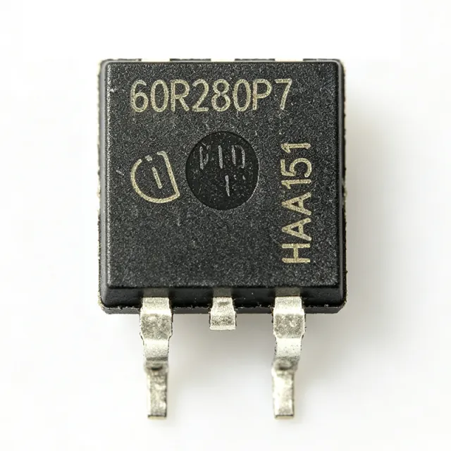
IPB60R280P7ATMA1 - 600V 280mOhm CoolMOS P7 MOSFET | Infineon
The Infineon IPB60R280P7ATMA1 is a 600 V N-channel power MOSFET from the CoolMOS P7 superjunction family, rated at 280 mOhm typical R_DS(on) and 12 A continuous drain current, housed in a surface-mount PG-TO263-3 (D2PAK) package. Built on Infineon's 7th-generation superjunction (SJ) principle, it pairs the fast-switching behavior of SJ MOSFETs with low ringing tendency and improved ease-of-use compared to the P6 generation. The device is specified for 600 V drain-source breakdown, 53 W power dissipation at T_C = 25 °C, and surface-mount mounting, making it a strong fit for compact, high-efficiency switched-mode power supplies. A power MOSFET is a voltage-controlled semiconductor switch that regulates current flow between the drain and source terminals in response to a gate-source voltage. Within the power semiconductor hierarchy, MOSFETs sit alongside IGBTs and thyristors as the dominant switching devices in modern SMPS designs, and superjunction MOSFETs in particular are the technology of choice for high-voltage (>500 V) AC-DC and DC-DC conversion because they simultaneously deliver low on-state loss, fast switching, and robust avalanche capability. The IPB60R280P7ATMA1 belongs to the 600 V CoolMOS P7 family, an industrial-grade successor to the widely-deployed P6 line. Key features include the 600 V drain-source breakdown voltage (V_DSS), 280 mOhm maximum R_DS(on) at V_GS = 10 V, an integrated gate-source threshold around 3.5 V suitable for standard gate-drive levels, and ultra-low ringing tendency that simplifies EMI filter design. The D2PAK (PG-TO263-3) package offers a large metal tab for direct PCB heatsinking, enabling sustained 12 A operation with proper thermal management. Compared with planar MOSFETs in the same voltage class, the SJ architecture typically yields 30-50% lower switching losses and reduced gate charge, translating directly into higher system efficiency. Typical applications include switched-mode power supplies (SMPS) for telecom and server auxiliary rails, PC silver-box and TV main power, solar inverters, industrial LED drivers, and e-mobility charging. The wide V_DS margin also allows usage in three-phase PFC front ends and hard-switching topologies up to ~150 kHz. When designing with this part, ensure the PCB copper-pour area is sized for the continuous drain current at the target R_DS(on) and that gate-drive loops are minimized to control EMI. Use a TVS across the drain-source path when inductive loads or transformer leakage spikes are present. This page synthesizes Infineon datasheet specifications, current distributor pricing and stock (as of 2026-09-14), pin-compatible drop-in alternatives, and practical design notes not consolidated in the manufacturer datasheet.
IPB65R041CFD7ATMA1 - 650V 41mΩ CoolMOS CFD7 MOSFET | Infineon
The Infineon IPB65R041CFD7ATMA1 is a 650V N-channel power MOSFET from the CoolMOS™ CFD7 family, delivering 50A continuous drain current and an ultra-low 41 mΩ maximum on-resistance in a surface-mount PG-TO263-3 (D2PAK) package. It dissipates up to 227W at Tc=25°C, with a fast body diode designed for resonant switching topologies such as LLC half-bridge and phase-shift full-bridge converters. The CFD7 generation succeeds the CFD2 platform, providing higher efficiency, lower switching losses, and a robust intrinsic body diode for hard-commutation duty. A power MOSFET is a voltage-controlled semiconductor switch that regulates or converts electrical energy by turning a drain-source current on and off in response to a gate-source voltage. Within the power-converter hierarchy, MOSFETs sit one level below magnetics, capacitors, and gate drivers; high-voltage superjunction types such as CoolMOS CFD7 are typically chosen for PFC, half-bridge, and full-bridge stages in switched-mode power supplies. Synonyms include N-channel MOSFET, superjunction MOSFET, and high-voltage FET. Industry standards governing this part family include JEDEC JESD22 for environmental robustness and IPC-A-610 for assembly acceptance. Key features of the IPB65R041CFD7ATMA1 include a 41 mΩ maximum R_DS(on) at V_GS=10V, a 650V drain-source breakdown voltage, integrated fast body diode with low Q_rr, low gate charge Q_G for reduced driver losses, and an avalanche-rated single-pulse body diode suitable for ZVS bridges. The device is part of Infineon's 500V-950V CFD7 portfolio and is halogen-free, RoHS-compliant, and qualified to JEDEC moisture sensitivity level 1. Technically, the CoolMOS CFD7 cell uses Infineon's superjunction structure with charge-balance compensation, achieving a per-area R_DS(on) that is several times lower than conventional planar MOSFETs of the same voltage class. The fast body diode uses lifetime-control techniques, making it safe for bridge topologies where the diode conducts before channel turn-on. Designers gain higher switching frequencies, smaller magnetics, and lower EMI. Typical applications include server and telecom SMPS, solar inverters, EV on-board chargers, industrial welding, and high-power LED drivers. The combination of low R_DS(on), 650V rating, and a robust body diode makes the IPB65R041CFD7ATMA1 especially well suited to LLC resonant converters and ZVS phase-shift full-bridge converters used in high-power-density AC-DC and DC-DC power supplies. When designing with this part, observe the 650V maximum V_DS and keep the avalanche energy below the datasheet single-pulse rating. Use a low-inductance gate-drive loop and minimize source-lead parasitic inductance to control switching loss and ringing. Always verify thermal performance with a board-level measurement rather than relying solely on R_thJC data. This page synthesizes distributor pricing, drop-in alternatives, and practical design notes not found in the manufacturer datasheet, helping engineers select and source the IPB65R041CFD7ATMA1 with confidence for next-generation high-efficiency power conversion designs.
IPB70N10S3L12ATMA1 - 100V 70A 11.8mΩ OptiMOS N-Ch MOSFET | Infineon
The Infineon IPB70N10S3L12ATMA1 is an N-channel enhancement-mode automotive OptiMOS power MOSFET rated at 100 V VDS, 70 A continuous drain current at 25 °C case temperature, and 11.8 mΩ maximum R<sub>DS(on)</sub>, housed in a surface-mount PG-TO263-3-2 (D2PAK) package with a 125 W power dissipation rating. It is qualified to AEC-Q101, MSL1 to 260 °C peak reflow, 175 °C operating junction temperature, RoHS compliant (green product), and 100 % avalanche tested. The S3L-12 die combines low switching and conduction losses for high thermal efficiency in a robust D2PAK footprint used across automotive 48 V systems. A power MOSFET is a voltage-controlled three-terminal semiconductor switch that uses the field effect of an insulated gate to modulate conduction between source and drain. It belongs to the family of discrete power semiconductors, sits above single transistors in the hierarchy (transistor → FET → MOSFET → power MOSFET → OptiMOS automotive grade), and forms the basic building block of all switched-mode power conversion, motor drive, and load switching topologies. The OptiMOS platform is Infineon's low-voltage MOSFET line targeting high-current density and low gate charge. Key features include 11.8 mΩ maximum R<sub>DS(on)</sub> at V<sub>GS</sub>=10 V for minimal conduction loss, a peak current capability of 180 A for inrush and transient handling, 100 % avalanche-rated switching for unclamped inductive load robustness, and ultra-low gate charge for fast switching at high frequency. The combination reduces both I²R losses and switching losses, allowing smaller magnetics and cooler operation in 48 V automotive and industrial designs. The S3L-12 die uses Infineon's advanced planar OptiMOS technology, which optimizes the cell pitch and epitaxial profile to balance on-resistance, gate charge, and avalanche energy. The exposed metal tab of the D2PAK package provides a very low thermal resistance path to the PCB or external heatsink, sustaining 125 W of dissipation when properly mounted. The logic-level gate threshold also makes the part directly compatible with microcontroller-driven low-voltage gate drivers. Typical applications include 48 V automotive inverter and DC-DC converter stages, high-current motor drives (EPS, fans, pumps), industrial switched-mode power supplies, battery management ORing and protection switches, and high-power synchronous rectification. The AEC-Q101 qualification makes the device particularly suited to on-vehicle power electronics that must survive harsh temperature and vibration profiles. When designing with this part, ensure the PCB copper area under the D2PAK tab is sufficient to keep junction temperature below 175 °C under worst-case continuous load. A low-impedance gate drive (≤10 Ω source resistance) is recommended to control switching losses and limit ringing. For 48 V bus systems, observe the V<sub>DS</sub> derating guideline and add adequate snubbing across inductive loads to stay within the avalanche rating. This page synthesizes distributor pricing, parametric same-package alternatives, and practical D2PAK thermal design notes that complement the manufacturer datasheet.
IPB70N10S3L12ATMA2 - 100V 70A N-Ch MOSFET, 11.8mΩ | Infineon
The Infineon IPB70N10S3L12ATMA2 is an N-channel OptiMOS-T power MOSFET rated at 100V VDS, 70A continuous drain current (Tc), and an exceptionally low R<sub>DS(on)</sub> of 11.8 mΩ, housed in a PG-TO263-3-2 (D2PAK) surface-mount package. It is part of Infineon's automotive-grade OptiMOS-T family optimized for 48V inverter and DC-DC converter applications. A power MOSFET (Metal-Oxide-Semiconductor Field-Effect Transistor) is a voltage-controlled switch used for high-efficiency power conversion. MOSFETs sit within the broader taxonomy of discrete semiconductors -> transistors -> FETs -> power MOSFETs. The OptiMOS-T family targets synchronous rectification, motor control, and high-current switching in automotive and industrial power systems. Key features include an 11.8 mΩ maximum on-resistance at V<sub>GS</sub> = 10V, 125W power dissipation at Tc, and AEC-Q101 automotive qualification with a 175°C maximum operating junction temperature. The device is 100% avalanche-tested, RoHS-compliant (Green product), and qualified to 260°C peak reflow profile per JEDEC J-STD-020. Technically, the IPB70N10S3L12ATMA2 uses Infineon's trench MOSFET technology with optimized cell density to balance conduction loss and switching performance. Its low gate charge and low Q<sub>rr</sub> minimize switching losses in high-frequency DC-DC converters, while the low R<sub>DS(on)</sub> reduces conduction losses in continuous-current paths such as motor phase switching. Typical applications include 48V automotive inverters, high-current DC-DC converters, motor drives for electric power steering (EPS) and water pumps, battery management protection circuits, and industrial synchronous rectification stages. Its AEC-Q101 qualification makes it suitable for safety-critical automotive subsystems. When designing with this MOSFET, ensure the gate driver delivers ≥10V V<sub>GS</sub> to fully enhance the channel, and select a TVS diode or snubber to manage avalanche energy. Thermal design must keep junction temperature below 175°C at full load, accounting for the D2PAK package's thermal resistance. This page synthesizes verified distributor pricing, drop-in alternatives, and practical design notes not found in the manufacturer datasheet alone.
IPB90N06S4L04ATMA2 - 60V 90A N-Ch MOSFET D2PAK | Infineon
The Infineon IPB90N06S4L04ATMA2 is an automotive-grade N-channel enhancement-mode MOSFET built on Infineon's OptiMOS T2 technology, rated at 60 V drain-source breakdown, 90 A continuous drain current (Tc), and 150 W power dissipation in a surface-mount PG-TO263-3-2 (D2PAK) package. It delivers a world-class on-state resistance of 3.4 mΩ typical at VGS=10 V, with the lowest conduction losses in its 60 V class. A power MOSFET (Metal-Oxide-Semiconductor Field-Effect Transistor) is a voltage-controlled three-terminal switch used for high-efficiency power conversion. The N-channel variant is the most common polarity and requires a positive gate drive. MOSFETs sit in the discrete semiconductor hierarchy alongside IGBTs and BJTs, and within power-electronics families they are subdivided into trench MOSFETs, planar MOSFETs, and HEMTs. The IPB90N06S4L04ATMA2 is a trench MOSFET, leveraging deep-trench cell geometry to minimise on-state resistance per unit silicon area. Key features include 3.4 mΩ R_DS(on) (typ) at VGS=10 V, 60 V V_DSS, 90 A I_D continuous, 150 W P_D, AEC-Q101 automotive qualification, 100% avalanche-tested, MSL1 moisture sensitivity rating up to 260 °C peak reflow, and 175 °C maximum operating temperature. The device is also Green Product (RoHS compliant) and Halogen-Free, meeting modern automotive environmental requirements. The trench-cell architecture enables industry-leading figure-of-merit (FOM = R_DS(on) × Q_g), reducing both switching and conduction losses. The result is higher system efficiency, lower thermal rise, and the ability to shrink heatsinks in space-constrained automotive ECUs, DC-DC converters, and motor-drive stages. Typical applications include automotive 12 V and 24 V high-current switching, electric power steering (EPS), braking systems, transmission control, body electronics, DC-DC converter stages, and motor drives. The low R_DS(on) and AEC-Q101 qualification make it especially well suited for direct-to-battery automotive loads where cold-crank and load-dump transients must be tolerated. Design tip: keep the gate-drive loop (gate resistor + driver) compact to suppress ringing, and add a TVS across the gate-source if the gate is exposed to fault transients. Always derate to ≤80% of the absolute-maximum ratings for production designs. This page synthesises distributor pricing, AEC-Q101-qualified drop-in alternatives, and practical thermal design notes not found in the bare manufacturer datasheet.

IPC100N04S51R7ATMA1 - 40V 100A OptiMOS-5 N-FET | Infineon
The Infineon IPC100N04S51R7ATMA1 is an N-channel enhancement-mode power MOSFET built on Infineon's OptiMOS-5 40 V technology, housed in a surface-mount PG-TDSON-8-34 (SS08 leadless) package. It is rated for a drain-source voltage VDS of 40 V, a continuous drain current ID of 100 A at case temperature TC, and a maximum power dissipation of 115 W at TC, with a junction-to-case thermal resistance of approximately 1.3 K/W allowing the silicon die to carry up to 193 A at 25 °C. A power MOSFET is a voltage-controlled semiconductor switch that uses an electric field at the gate to modulate conduction between the drain and source terminals. Within the discrete-semiconductor hierarchy, MOSFETs sit under transistors and serve as the workhorse switching element in DC-DC converters, motor drives, and load switches. The OptiMOS-5 family targets best-in-class figure-of-merit (FOM = RDS(on) x Qg), giving system designers lower conduction and switching losses compared to older generations. Key features of this part include AEC-Q101 automotive qualification, 100% avalanche-tested silicon, MSL1 rating to 260 °C peak reflow, a 175 °C maximum operating junction temperature, and RoHS-compliant lead-free terminations. The PG-TDSON-8-34 footprint exposes the drain via the thermal pad, which slashes package resistance and inductance versus traditional DPAK packages. OptiMOS-5 40 V is optimized for 12 V and 24 V automotive subsystems such as ECU power rails, body electronics, electric power steering, and braking modules. The combination of very low on-resistance and high pulsed current handling makes the device equally suited to high-current synchronous rectification in 48 V mild-hybrid DC-DC stages and to battery-protection disconnect switches in e-mobility applications. When designing with this device, observe safe operating area (SOA) by derating current with temperature; the 100 A rating applies at TC and falls as TC rises. Place the gate driver within a few millimeters of the gate pin to suppress ringing, and provide a low-impedance Kelvin source connection whenever possible. This page synthesizes distributor pricing, drop-in alternatives, and practical design notes that complement the manufacturer datasheet.
IPC100N04S52R8ATMA1 - 40V 100A N-Ch OptiMOS MOSFET | Infineon
The Infineon IPC100N04S52R8ATMA1 is an N-channel OptiMOS power MOSFET rated at 40V VDS and 100A continuous drain current (Tc), dissipating up to 75W (Tc) in a surface-mount PG-TDSON-8-34 package. AEC-Q101 qualified for automotive applications, it combines low on-state resistance with 100% avalanche testing and 175C operating temperature capability, making it suitable for harsh-environment automotive power conversion. A power MOSFET (Metal-Oxide-Semiconductor Field-Effect Transistor) is a voltage-controlled three-terminal device used as a fast electronic switch or amplifier in power circuits. N-channel MOSFETs conduct between drain and source when a positive gate-source voltage exceeds the threshold, and they sit within the broader transistor -> discrete semiconductor -> semiconductor taxonomy. OptiMOS is Infineon's trench MOSFET technology platform that minimizes RDS(on) and gate charge to maximize efficiency in switching applications. Key features include an exceptionally low typical on-state resistance of approximately 2.8 mOhm at VGS=10V, AEC-Q101 automotive qualification with MSL1 (260C peak reflow) robustness, and an operating junction temperature range of -55C to +175C. The PG-TDSON-8-34 package features an exposed drain pad (EP) that provides a low thermal resistance path to the PCB, allowing the device to sustain high continuous currents when properly mounted on adequate copper area. The part is Green Product (RoHS compliant) and 100% avalanche-tested per Infineon reliability standards. Technically, the IPC100N04S52R8ATMA1 is built on OptiMOS 5 40V technology, employing a shielded-gate trench structure that simultaneously reduces conduction loss (RDS(on) * ID) and switching loss (driven by gate charge Qg and output capacitance Coss). The 8-pin TDSON-8-34 footprint is the standard Infineon high-current automotive MOSFET outline used across 40V, 60V, and 100V OptiMOS families, enabling easy migration between voltage grades. Typical applications include automotive 12V/24V battery switching, DC-DC converter high-side switches, motor drive H-bridges (12V automotive loads such as seat motors, window lifters, and fuel pumps), solenoid drivers, and reverse-polarity protection circuits. The combination of low RDS(on), high current rating, and automotive qualification also suits e-mobility 48V mild-hybrid auxiliary systems and industrial switched-mode power supplies that must survive automotive-grade transients. When designing with this device, allocate at least 1 cm^2 of 2 oz copper on the drain pad to keep junction-to-ambient thermal resistance within usable bounds at full load. Gate drive should use a 10V enhancement supply with a gate resistor of 10-47 Ohm to control switching dV/dt and limit ringing on long gate traces.
IPC100N04S5L1R1ATMA1 - 40V 100A OptiMOS-5 N-Channel MOSFET | Infineon
The Infineon IPC100N04S5L1R1ATMA1 is a 40 V N-channel enhancement-mode power MOSFET from Infineon's OptiMOS-5 40 V family, delivering 100 A continuous drain current (at TC) with an ultra-low typical on-resistance of 1.1 mΩ, housed in the leadless PG-TDSON-8-34 (SS08) surface-mount package. It is qualified to AEC-Q101 for automotive applications, supports MSL1 to 260 °C peak reflow, and is rated for a 175 °C operating junction temperature with 100% avalanche tested ruggedness. A power MOSFET (Metal-Oxide-Semiconductor Field-Effect Transistor) is a voltage-controlled switch used to efficiently switch or amplify power in electronic circuits. The N-channel enhancement mode means the device is normally OFF at VGS=0 and turns ON when a positive gate-source voltage is applied. The OptiMOS-5 family is Infineon's 5th-generation 40 V trench MOSFET platform, sitting within the broader taxonomy: power MOSFET -> discrete semiconductor -> power transistor -> semiconductor device. Logic-level gate drive (VGS(th) ~1-2 V typical) allows direct PWM control from microcontrollers, gate drivers, or 3.3 V/5 V logic without a charge pump. Key features include best-in-class figure-of-merit (FOM = RDS(on) × Qg), low package resistance and inductance thanks to the SS08 leadless footprint, AEC-Q101 automotive qualification, MSL1 floor-life unlimited up to 260 °C reflow, 175 °C maximum operating temperature, and 100% avalanche-tested ruggedness. The Green Product (RoHS-compliant) construction supports modern lead-free assembly. The OptiMOS-5 40 V technology delivers best-in-class switching performance and lower conduction losses, which translates directly into higher efficiency, smaller magnetics, and reduced thermal budgets in high-current 12 V/24 V automotive and industrial designs. The low-inductance SS08 package minimizes voltage overshoot during hard switching at high di/dt. Typical applications include automotive 12 V/24 V ECUs, electric power steering (EPS), transmission control units (TCU), battery management systems (BMS), DC-DC converters, and motor drive half-bridges. Designers select this part when the system demands high current, ultra-low conduction loss, AEC-Q101 reliability, and a small footprint. A key design consideration is thermal management: at 100 A into a 1.1 mΩ RDS(on), conduction loss alone is 11 W, so an extensive PCB copper pour or external heatsink is mandatory. The 8-pin TDSON exposed pad must be soldered to a sufficiently large thermal land to keep Tj below 175 °C. This page synthesizes distributor pricing, drop-in alternatives including same-brand and cross-brand options, and practical design notes not found in the manufacturer datasheet alone, enabling faster design-in decisions.
IPC100N04S5L1R5ATMA1 - 40V 100A OptiMOS-5 N-MOSFET | Infineon
The Infineon IPC100N04S5L1R5ATMA1 is an automotive-grade N-channel power MOSFET built on Infineon's OptiMOS-5 40 V technology, housed in a PG-TDSON-8-34 (SS08 leadless) surface-mount package with exposed pad. It delivers a continuous drain current of 100 A at Tc and a power dissipation of 115 W at Tc, with an extremely low typical on-resistance of 1.5 mΩ at VGS=10 V and 1.8 mΩ at VGS=4.5 V, optimized for high-current, low-loss switching. A power MOSFET is a voltage-controlled semiconductor switch that uses an electric field applied to the gate terminal to control current flow between drain and source. OptiMOS-5 represents Infineon's fifth-generation trench MOSFET platform, offering best-in-class figure-of-merit (FOM = RDS(on) × Qg), lower package resistance and inductance, and improved switching performance versus prior generations. This part occupies the upper tier of the OptiMOS-5 40 V family alongside IPC100N04S5L-1R1 (1.1 mΩ). It is a member of the broader power MOSFET family within discrete semiconductors, sitting above generic trench MOSFETs and below wide-bandgap GaN/SiC devices in performance-per-watt. Key features include logic-level drive (fully enhanced at VGS=4.5 V), AEC-Q101 qualification for automotive use, MSL1 moisture sensitivity up to 260 °C peak reflow, 175 °C maximum operating junction temperature, RoHS-compliant green product construction, and 100% avalanche-tested ruggedness. The SS08 leadless package minimizes parasitic source inductance, which directly reduces switching losses in high-frequency applications. Architecturally, the device uses an enhancement-mode N-channel trench cell structure optimized for low RDS(on) per unit silicon area. At VDS=20 V and ID=50 A pulsed, the typical on-resistance reaches its datasheet figure of merit. The gate charge is balanced against output capacitance to give low switching loss in both hard-switched and soft-switched topologies. Avalanche ruggedness is verified at 100% on production units, providing margin against unclamped inductive switching events such as load-dump transients in automotive environments. Typical applications include automotive 12 V and 24 V high-current switching such as EPS (electric power steering) motors, electronic parking brakes, brake-by-wire systems, transmission control units, battery management and protection OR-ing, hot-swap controllers, BLDC motor drives for pumps and fans, DC-DC converter synchronous rectification, and industrial high-current solenoid driving. The wide SOA at 175 °C operation also supports under-hood and chassis-mount designs with restricted cooling. When designing with this device, ensure that the gate drive can source/sink sufficient peak current to achieve sub-100 ns switching at full load, and place the gate driver as close to the gate pad as possible to minimize the gate-loop inductance. A 10 Ω gate resistor is recommended to dampen ringing. For OR-ing, add a TVS across the drain-source path to absorb avalanche energy beyond the device's rating. The exposed pad must be soldered to a sufficiently large copper pour to keep RDS(on) rise from self-heating within safe margins.
IPC50N04S55R8ATMA1 - 40V 50A OptiMOS 5 N-FET | Infineon
The Infineon IPC50N04S55R8ATMA1 is an N-channel enhancement-mode OptiMOS 5 power MOSFET rated at 40 V drain-source voltage and 50 A continuous drain current (Tc), dissipating up to 42 W (Tc), packaged in a surface-mount PG-TDSON-8-33 (TDSON EP) outline with 5.8 mΩ typical R_DS(on). According to Infineon's product family datasheet, the part is AEC-Q101 qualified for automotive applications, MSL1 rated up to 260 °C peak reflow, and 100% avalanche tested, with a 175 °C maximum operating junction temperature. What is an N-channel power MOSFET? An N-channel MOSFET (metal-oxide-semiconductor field-effect transistor) is a voltage-controlled switch that uses an N-type conducting channel between drain and source. Power MOSFETs like the OptiMOS 5 family sit in the discrete semiconductor hierarchy: MOSFET -> FET -> transistor -> discrete semiconductor. They are the workhorse switching elements in DC-DC converters, motor drives, and load switches where high efficiency, low conduction loss, and fast switching are required. The 40 V rating positions this part in the low-voltage synchronous-rectification tier commonly used in 12 V automotive and 24 V industrial rails. Key features of the IPC50N04S55R8ATMA1 include an ultra-low typical R_DS(on) of 5.8 mΩ at 10 V VGS, a logic-level compatible gate threshold, and a 305 pF output capacitance figure that allows fast switching transitions. The TDSON-8-33 package exposes the drain through a large thermal pad, giving a junction-to-case thermal resistance well below standard SO-8 equivalents and enabling continuous high-current operation without a separate heatsink. Architecturally, the OptiMOS 5 platform uses Infineon's latest trench-technology cell design, balancing on-resistance, gate charge, and figure-of-merit (FOM = R_DS(on) × Qg) for synchronous-rectification and hot-swap applications. The result is a part that drops less power than its predecessors while accepting the same gate-drive rails. Typical applications include automotive 12 V ECU switching, eMobility load management, OR-ing and hot-swap controllers, and high-current DC-DC converter synchronous-rectifier stages. The AEC-Q101 qualification makes it directly suitable for under-hood and chassis electronics where automotive reliability is mandatory. When designing with this MOSFET, ensure the gate-drive voltage reaches at least 10 V for full enhancement, and place the gate-driver as close to the gate pin as possible to minimize the parasitic loop inductance that limits switching speed. This page synthesizes distributor pricing, drop-in alternatives, and practical design notes not found in the manufacturer datasheet alone.
IPC50N04S5L5R5ATMA1 - 40V 50A 5.5mΩ OptiMOS Auto MOSFET | Infineon
The Infineon IPC50N04S5L5R5ATMA1 is an N-channel enhancement-mode logic-level power MOSFET from Infineon's OptiMOS™ automotive family, rated at 40 V VDS, 50 A continuous drain current (Tc) and 5.5 mΩ maximum RDS(on) at 10 V VGS, housed in a surface-mount PG-TDSON-8-33 (TDSON EP 8-pin) package with exposed thermal pad. The part is AEC-Q101 qualified, MSL1 rated, supports 260 °C peak reflow, and operates across a 175 °C junction temperature range, making it suitable for under-the-hood and other harsh-environment automotive loads. A power MOSFET is a voltage-controlled three-terminal semiconductor switch that conducts current between drain and source when a sufficient gate-source voltage is applied. N-channel enhancement-mode MOSFETs (the most common type) are normally OFF at zero VGS, then turn ON when VGS exceeds the threshold, and are widely used in synchronous buck converters, motor drives, solenoid drivers, and reverse-battery protection blocks in 12 V and 24 V automotive systems. The OptiMOS™ family specifically targets low RDS(on) per die area and fast switching, optimizing conduction and switching losses for high-current, high-frequency DC-DC conversion. Key features of the IPC50N04S5L5R5ATMA1 include 5.5 mΩ max RDS(on) at VGS=10 V, logic-level compatibility (full enhancement at VGS as low as 4.5 V), 100 % avalanche-rated design, RoHS-compliant green-product construction, and a low RthJC of 3.6 K/W allowing the silicon die to carry up to 60 A at 25 °C case before package-limited current derating applies. The TDSON-8-33 footprint exposes the drain tab for top-side cooling, which is critical at the 42 W (Tc) power dissipation rating. Architecturally, this device uses Infineon's trench MOSFET process with an optimized cell pitch that minimizes figure-of-merit RDS(on)×Qg. This enables high-efficiency switching at high frequencies (typically 100 kHz to 1 MHz in DC-DC stages) without the gate-charge penalty seen in older planar processes. The exposed pad also reduces thermal resistance, supporting high continuous currents on a small PCB footprint. Typical applications include automotive 12 V and 24 V high-current switching (ECUs, body control modules), motor and solenoid drivers for HVAC flaps and pumps, synchronous rectification in secondary-side DC-DC converters, reverse-battery protection MOSFETs, hot-swap and OR-ing circuits, and industrial 24 V bus switches. Its AEC-Q101 qualification makes it especially attractive for safety-relevant automotive designs. When designing with this MOSFET, keep gate-drive rise/fall times short (use a dedicated gate driver such as the EiceDRIVER™ 1ED family) and minimize loop inductance between drain, source and the gate-driver return. Thermal management must account for both steady-state conduction (P = I² × RDS(on)) and switching losses, especially at VIN near 24 V where avalanche energy during load-dump events must be dissipated within the avalanche rating. This page synthesizes distributor pricing, drop-in alternatives, and practical design notes not found on the manufacturer datasheet cover page, providing information gain for engineers selecting an automotive-grade 40 V N-channel MOSFET for body and powertrain applications.
IPC70N04S5L4R2ATMA1 - 40V 70A OptiMOS 5 N-Ch MOSFET | Infineon
The Infineon IPC70N04S5L4R2ATMA1 is an N-channel 40 V OptiMOS 5 power MOSFET rated for 70 A continuous drain current (Tc) and 50 W power dissipation, housed in a PG-TDSON-8-34 surface-mount package with an exposed drain pad. It features an ultra-low typical R_DS(on) of 4.2 mΩ at 10 V Vgs and is logic-level compatible (4.5 V drive), AEC-Q101 qualified for automotive applications, MSL1 rated to 260°C peak reflow, and rated for 175°C operating junction temperature. The device is 100% avalanche-tested and is a Green Product (RoHS compliant). A power MOSFET is a voltage-controlled semiconductor switch used to efficiently route or modulate current in power-conversion circuits. N-channel MOSFETs, in particular, dominate high-current switching applications because electrons (the majority carrier) provide lower on-resistance than p-channel equivalents. OptiMOS 5 is Infineon's fifth-generation 40 V-300 V trench MOSFET platform, engineered to minimize switching and conduction losses simultaneously. This part sits in the broader power-management hierarchy: power MOSFET -> discrete semiconductor -> power electronics -> system-level power tree. Key features that differentiate this part include its industry-leading figure of merit (R_DS(on) x Q_g) thanks to the OptiMOS 5 cell design, an integrated source-drain body diode optimized for low Q_rr, and a logic-level gate threshold that enables direct drive from 3.3 V-5 V microcontrollers without a gate-driver stage. The combination of 4.2 mΩ R_DS(on) and 70 A continuous current in the compact TDSON-8-34 footprint delivers high power density, suitable for space-constrained automotive ECU boards. The IPC70N04S5L4R2ATMA1 is AEC-Q101 qualified, MSL1, and 100% avalanche-tested, indicating it has been validated for harsh automotive electrical environments including load-dump, jump-start, and reverse-battery transients. The 175°C junction temperature rating provides a wide thermal envelope for under-hood or near-engine placement. Typical applications include automotive 12 V/24 V high-current switching (e.g., ECU power distribution, motor drive H-bridges, LED matrix drivers, and battery-management OR-ing switches), industrial buck/boost converter high-side switches, and high-current USB-PD load switches. The 4.2 mΩ R_DS(on) keeps conduction losses below 1% even at 50 A load. When designing with this MOSFET, ensure Vgs is held above 6 V for full enhancement under all conditions (logic-level is for turn-on only; full R_DS(on) is specified at Vgs = 10 V). The exposed drain pad must be soldered to a sufficiently large copper pour to keep thermal resistance (R_theta_JA) within design budgets. Use a gate-resistor to dampen parasitic ringing, especially in motor-drive circuits where dV/dt can couple back through C_gd. This page synthesizes distributor pricing, drop-in pin-compatible alternatives, and practical design notes not found in the manufacturer datasheet alone.