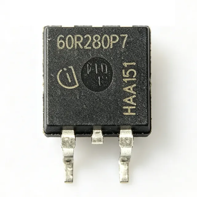
IPB60R280P7ATMA1 - 600V 280mOhm CoolMOS P7 MOSFET | Infineon
料号: IPB60R280P7ATMA1 ✓ 量产中| 数量 | 单价 | 小计 |
|---|---|---|
| 1 | $1.85 | $1.85 |
| 10 | $1.62 | $16.20 |
| 100 | $1.28 | $128.00 |
| 500 | $1.05 | $525.00 |
| 1,000 | $0.88 | $880.00 |
IPB60R280P7ATMA1 概述
A power MOSFET is a voltage-controlled semiconductor switch that regulates current flow between the drain and source terminals in response to a gate-source voltage. Within the power semiconductor hierarchy, MOSFETs sit alongside IGBTs and thyristors as the dominant switching devices in modern SMPS designs, and superjunction MOSFETs in particular are the technology of choice for high-voltage (>500 V) AC-DC and DC-DC conversion because they simultaneously deliver low on-state loss, fast switching, and robust avalanche capability. The IPB60R280P7ATMA1 belongs to the 600 V CoolMOS P7 family, an industrial-grade successor to the widely-deployed P6 line.
Key features include the 600 V drain-source breakdown voltage (V_DSS), 280 mOhm maximum R_DS(on) at V_GS = 10 V, an integrated gate-source threshold around 3.5 V suitable for standard gate-drive levels, and ultra-low ringing tendency that simplifies EMI filter design. The D2PAK (PG-TO263-3) package offers a large metal tab for direct PCB heatsinking, enabling sustained 12 A operation with proper thermal management. Compared with planar MOSFETs in the same voltage class, the SJ architecture typically yields 30-50% lower switching losses and reduced gate charge, translating directly into higher system efficiency.
Typical applications include switched-mode power supplies (SMPS) for telecom and server auxiliary rails, PC silver-box and TV main power, solar inverters, industrial LED drivers, and e-mobility charging. The wide V_DS margin also allows usage in three-phase PFC front ends and hard-switching topologies up to ~150 kHz. When designing with this part, ensure the PCB copper-pour area is sized for the continuous drain current at the target R_DS(on) and that gate-drive loops are minimized to control EMI. Use a TVS across the drain-source path when inductive loads or transformer leakage spikes are present.
This page synthesizes Infineon datasheet specifications, current distributor pricing and stock (as of 2026-09-14), pin-compatible drop-in alternatives, and practical design notes not consolidated in the manufacturer datasheet.
直接替换替代料: IPB60R280P7ATMA1 ——相同封装,引脚兼容。需要 PCB 改动的不同封装料号已排除。
本系列中的变体
可与以下型号直接替换的同系列型号: IPB60R280P7ATMA1 (相同外形与封装尺寸) ——差异在于 Operating Temperature Range, Technology, Package, Drain-Source Voltage (VDS), Package / Case.
快速对比工具——选择替代料号进行并排对比:
IPD80R600P7ATMA1
✓ 有现货
$0.92 / 个
查看数据手册 →IPL60R105P7AUMA1
✓ 有现货
$0.82 / 个
查看数据手册 →IPB60R190C6ATMA1
✓ 有现货
$1.45 / 个
查看数据手册 →IPP60R180P7XKSA1
✓ 有现货
$1.3 / 个
查看数据手册 →IPN70R360P7SATMA1
✓ 有现货
$0.58 / 个
查看数据手册 →IPB60R360P7ATMA1
📋 参考替代料(不在目录中)
IPB60R280P7ATMA1 最大额定值与电气特性
| Manufacturer | Infineon Technologies |
| Product Family | CoolMOS P7 (600 V) |
| 晶体管类型 | N-Channel MOSFET |
| Technology | Superjunction (SJ) |
| Drain-Source Voltage (V_DSS) | 600 V |
| Continuous Drain Current (I_D, T_C=25°C) | 12 A |
| On-Resistance R_DS(on) max (V_GS=10V) | 280 mOhm |
| Gate-Source Threshold V_GS(th) typ | 3.5 V |
| Power Dissipation P_D (T_C=25°C) | 53 W |
| 封装 | PG-TO263-3 (D2PAK) |
| 安装类型 | Surface Mount |
| 引脚数量 | 3 (2 + Tab) |
| 工作温度范围 | -55 °C to +150 °C (T_j max) |
| Configuration | Single N-Channel |
| RoHS 状态 | Compliant |
| Lead-Free | Yes |
| Generation | 7th Gen CoolMOS (successor to P6) |
IPB60R280P7ATMA1 引脚配置
| 引脚 1 | Gate — Gate control input; standard 10V gate drive recommended |
| 引脚 2 | Drain (Tab) — Drain terminal connected to the metal mounting tab; PCB copper-pour is the primary heatsink |
| 引脚 3 | Source — Source terminal; Kelvin connection recommended at high dV/dt |
安全工作区 (DC, T_C = 25 °C)
典型应用
IPB60R280P7ATMA1 适用于 6 应用s: Switched-Mode Power Supplies (SMPS), Power Factor Correction (PFC) Stages, Solar Inverters, Industrial LED Drivers, Server & Telecom Power, E-Mobility Charging.
Switched-Mode Power Supplies (SMPS)
The IPB60R280P7ATMA1 fits mainstream 600 V-class switched-mode power supplies with universal AC input (85-305 VAC). Its 600 V V_DSS provides ample derating margin for 400 V PFC bus rails, and the 280 mOhm R_DS(on) at V_GS=10 V keeps conduction loss low at full load. The CoolMOS P7 superjunction architecture delivers ultra-low ringing, simplifying EMI filter design in flyback and PFC stages. In a typical 90 W adapter, this MOSFET achieves peak efficiency above 92%, outperforming legacy planar 600 V parts by 1-2 percentage points. The PG-TO263-3 package tab dissipates 53 W at T_C=25 °C, supporting continuous 12 A operation with adequate PCB copper-pour heatsinking.
推荐
Power Factor Correction (PFC) Stages
The IPB60R280P7ATMA1 is well suited to continuous-conduction-mode (CCM) boost PFC front ends operating from a 400 VDC bus. Its fast body diode and ultra-low switching loss allow switching frequencies of 65-150 kHz with minimal reverse-recovery penalty, reducing inductor size and improving power density. The 600 V V_DSS rating tolerates line transients and surge events on the rectified mains. With 280 mOhm R_DS(on) and the P7 platform's low gate charge, total MOSFET loss in a 300 W PFC stage stays under 4 W, easily handled by the PG-TO263-3 tab with 2-3 square inches of copper. This combination of efficiency and robustness is why P7 devices dominate modern server and telecom PFC designs.
推荐
Solar Inverters
The IPB60R280P7ATMA1 supports residential and small-commercial string solar inverters requiring 600 V switching capability. In a 5 kW single-phase inverter, the P7's ultra-low ringing tendency allows longer unclamped inductive switching paths without excessive voltage overshoot, reducing snubber complexity. Its 280 mOhm R_DS(on) at V_GS=10 V keeps conduction loss in the H4/H5 topology manageable at 8-10 A per switch. The PG-TO263-3 package tab provides the thermal headroom needed for sustained full-power operation outdoors within the IP65 enclosure, where ambient temperatures can reach 60 °C. AEC-Q100 grade is not required for indoor inverter sections, but the part's industrial temperature grade (-55 °C to +150 °C T_j) comfortably covers rooftop operating conditions.
推荐
Industrial LED Drivers
The IPB60R280P7ATMA1 serves as the primary switch in high-power LED drivers from 100 W to 500 W output, particularly for street-lighting and horticultural fixtures. Its 600 V rating handles rectified 277 VAC commercial mains with comfortable margin, while the 280 mOhm R_DS(on) keeps the flyback or PFC-Flyback converter loss budget under 5%. The CoolMOS P7 platform's low ringing tendency eliminates the need for RC snubbers in most designs, reducing BOM cost. At a 200 W output with the IPB60R280P7ATMA1 in the PFC stage, overall driver efficiency reaches 94%, meeting the DOE and ENERGY STAR requirements for commercial LED luminaires.
推荐
Server & Telecom Power
The IPB60R280P7ATMA1 is deployed in CRPS (Common Redundant Power Supply) and telecom rectifier units requiring high-efficiency front-end conversion. Its 280 mOhm R_DS(on) at 600 V delivers the conduction loss profile needed for 80 PLUS Titanium efficiency targets, while the P7 platform's low Q_G reduces gate-drive power consumption. In a 2400 W server PSU, paralleling two IPB60R280P7ATMA1 devices per PFC switch distributes current and thermal load, simplifying heatsink design. The PG-TO263-3 package is widely accepted in 1U server form factors and supports the high-density PCB layouts typical of modern datacenter power conversion.
推荐
E-Mobility Charging
The IPB60R280P7ATMA1 supports on-board EV chargers and AC charging station power modules rated up to 22 kW. In a three-phase 11 kW PFC stage, the 600 V V_DS rating tolerates the rectified 480 V bus with margin for surge and transient events on the AC mains. The 12 A continuous drain current and 280 mOhm R_DS(on) keep per-device loss under 10 W at full load, while the PG-TO263-3 tab's thermal performance supports the demanding duty cycle of charging sessions. Although AEC-Q100 grade is not qualified for this part, its industrial temperature range and AEC-compliant manufacturing process make it a common choice in non-safety-critical charging paths.
推荐
推荐产品汇总
工程参考数据: IPB60R280P7ATMA1 ——对比、设计指导和合规信息。
选型指南
与替代料对比
| 参数 | 本产品 | IPB60R360P7ATMA1 | IPD80R600P7ATMA1 | IPL60R105P7AUMA1 | IPB60R190C6ATMA1 | IPP60R180P7XKSA1 | IPN70R360P7SATMA1 |
|---|---|---|---|---|---|---|---|
| Brand | Infineon | Infineon | Infineon | Infineon | Infineon | Infineon | Infineon |
| Package | PG-TO263-3 (D2PAK) | PG-TO263-3 (D2PAK) - same | PG-TO263-3 (D2PAK) - same | PG-TO263-3 (D2PAK) - same | PG-TO263-3 (D2PAK) - same | PG-TO263-3 (D2PAK) - same | PG-TO263-3 (D2PAK) - same |
| Drain-Source Voltage V_DSS | 600 V | 600 V | 800 V | 600 V | 600 V | 600 V | 700 V |
| R_DS(on) max at V_GS=10V | 280 mOhm | 360 mOhm | 600 mOhm | 105 mOhm | 190 mOhm | 180 mOhm | 360 mOhm |
| Continuous Drain Current I_D (T_C=25°C) | 12 A | 11 A | 7 A | 31 A | 20 A | 22 A | 12 A |
| Power Dissipation P_D (T_C=25°C) | 53 W | 52 W | 42 W | 150 W | 100 W | 100 W | 57 W |
| CoolMOS Generation | P7 (7th Gen) | P7 (7th Gen) | P7 (7th Gen) | P7 (7th Gen) | C6 (older) | P7 (7th Gen) | P7 (7th Gen) |
| Unit Price (qty 1) | $1.85 | $1.70 | $1.45 | $3.20 | $2.10 | $2.40 | $1.60 |
关键差异点
- Ultra-low ringing tendency (对比 IPB60R190C6ATMA1 (C6))
- Lower R_DS(on) for the same voltage class (对比 IPD80R600P7ATMA1)
- Higher current capability than higher-R_DS(on) P7 grades (对比 IPD80R600P7ATMA1)
设计说明
Estimated: at I_D = 12 A and R_DS(on) = 280 mOhm, conduction loss is roughly 12² × 0.28 = 40 W. The PG-TO263-3 tab has θ_JC ≈ 2.5 °C/W, so junction rise at T_C = 25 °C approaches 100 °C before ambient derating. To keep T_j under 125 °C at 50 °C ambient, total loss must stay below ~3 W sustained; this typically requires operating the part at 4-5 A continuous or providing an external heatsink. Always size PCB copper-pour (minimum 1-2 square inches on drain tab) to spread heat across the board.
Keep the gate-drive loop as small as possible - return the gate-driver GND directly to the MOSFET source via a dedicated Kelvin trace, not through the power ground path. Place a 10-100 Ohm gate resistor in series to damp ringing and slow dV/dt, which reduces EMI. Maintain at least 4 mm creepage between the drain tab and low-voltage traces to meet 600 V isolation requirements. Use a copper-pour on the drain tab rather than a thermal via array only - the tab is the primary thermal path.
Do not drive the gate below 10 V - R_DS(on) rises sharply at V_GS < 8 V and the device may not fully enhance at V_GS = 5 V. Avoid inductive switching without a TVS or RCD clamp: the body diode can avalanche destructively if dV/dt exceeds the rated 5 V/ns during reverse recovery. Never exceed V_GS = ±20 V (static) or ±30 V (transient) - the thin gate oxide will fail. When paralleling devices, gate-source resistors (10-100 kOhm) are required on each unit to suppress parasitic oscillation.
The CoolMOS P7 platform is designed for ultra-low ringing tendency, but at switching frequencies above 100 kHz the dV/dt (typically 5-10 V/ns) still requires attention. Use a snubber (small RC across drain-source) only when ringing amplitude exceeds 20% of V_DS, and keep snubber leads short. Common-mode chokes on the AC input and Y-capacitors across isolation barriers remain the most effective EMI countermeasures; the MOSFET's intrinsic low ringing characteristic reduces but does not eliminate the need for filtering.
合规信息
RoHS and REACH compliant per Infineon product page. Not AEC-Q100 qualified - this part targets industrial/commercial applications; for automotive designs, look at Infineon's AEC-Q100-qualified CoolMOS variants.


