电源管理
子分类
产品(2819)

DML3006LFDS-7 - 11A Smart Load Switch | Diodes Inc | Power Distribution
The Diodes Incorporated DML3006LFDS-7 is a single-channel smart load switch housed in an 8-pin V-DFN2020-8 (Type F) package, integrating one N-channel MOSFET rated for up to 10.5A continuous current (datasheet maximum of 11A) across a 0.5V to 13.5V input voltage range. The device provides a component-and-area-reducing solution for efficient power domain switching, featuring programmable soft-start inrush-current limiting, ultra-low on-resistance, fault signaling, and a power-good (PG) indicator output. According to the Diodes Incorporated datasheet, the load switch's wide VIN range and high continuous-current capability enable use as a discrete replacement for a MOSFET plus discrete driver + protection circuitry combination. A load switch is a power-management IC that combines a power MOSFET with control, protection, and monitoring functions into a single package; it sits between a DC rail (such as a buck-converter output or battery) and a downstream load (SOC rail, peripheral, sensor, or memory). By integrating the gate driver, current-limit reference, fault comparator, and power-good logic, a smart load switch replaces 5-10 discrete components while providing inrush control, short-circuit protection, and rail-status telemetry that discrete MOSFETs cannot deliver on their own. Key features include an adjustable soft-start slew rate set by an external capacitor, programmable current-limit threshold, thermal-shutdown protection, and an open-drain power-good output that de-asserts on fault. The V-DFN2020-8 (Type F) package is a 2.0 mm x 2.0 mm DFN with an exposed thermal pad that lowers theta-JA, supporting the high continuous current in a minimal PCB footprint. The internal N-channel MOSFET is driven by an integrated charge-pump gate driver that holds VGS high across the full 0.5V to 13.5V input range - including sub-1V rails where a discrete logic-level N-FET would be marginal. This makes N-FLT power domains on 0.8V, 1.0V, 1.2V, 1.8V, 3.3V, and 5V buses all driveable from a single part. The PG output and ON pin allow sequencing in multi-rail systems. Typical applications include USB Type-C VBUS switching, SSD and eMMC power-domain control in mobile/embedded platforms, hot-swap power rails in networking switches, fan and motor power distribution, and battery-disconnect functions in portable IoT. The small V-DFN2020 footprint also suits wearable and AR/VR platforms where PCB area is constrained. When designing with the DML3006LFDS-7, place the soft-start capacitor as close as possible to the SS pin to control inrush accurately, and ensure the exposed pad receives at least four thermal vias to a ground copper pour so the device can sustain the full 10.5A continuous rating without triggering thermal shutdown. This page synthesizes distributor pricing, verified datasheet parameters, same-brand and cross-brand drop-in alternatives, and engineering design guidance not found in any single distributor listing.

DP83848I-POE-EK - DP83848I 10/100 PoE PHY Evaluation Kit | TI
The Texas Instruments DP83848I-POE-EK is the official evaluation board for the DP83848I PHYTER industrial-temperature single-port 10/100 Mb/s Ethernet Physical Layer Transceiver, packaged as a complete Power-over-Ethernet reference design. It integrates an isolated flyback DC/DC converter that delivers 3.3 V from the 48 V PoE input, allowing engineers to power the PHY directly from a PoE source without any external supply. The board exposes the MII/RMII interface, RJ-45 magnetics, and configuration jumpers so the user can exercise HP Auto-MDIX, Energy-Efficient Ethernet, and 10BASE-T/100BASE-TX link modes straight out of the box. An Ethernet PHY transceiver is the physical-layer device that sits between a digital MAC and the copper magnetics of an RJ-45 jack. It handles line coding, link-pulse detection, echo cancellation, and adaptive equalization so the MAC sees a clean MII/RMII bus. The DP83848I-POE-EK falls under Power Management > DC-DC Converters / Specialized Evaluation Boards, which itself sits inside the broader hierarchy of Power Management & Development Tools for industrial Ethernet, factory automation, and IP-camera designs. Key features include industrial-temperature operation from -40 °C to +85 °C, integrated PoE PD (powered device) interface compliant with IEEE 802.3af, an isolated single-output flyback DC/DC stage that produces 3.3 V at the load, programmable LED status indicators for link, speed, activity, and duplex, and on-board MSP430-grade headers for jumper configuration. The 10/100 Mb/s PHY core delivers cable diagnostics and Auto-MDIX for cross-over-cable-free operation. Deeper technical detail is provided in the architecture of the DC/DC stage: a current-mode flyback with primary-side regulation, 1500 V isolation, and synchronous switching chosen for thermal efficiency. The PHY itself uses TI's proprietary DSP-based echo canceller and baseline-wander correction, allowing it to exceed the IEEE 802.3 100BASE-TX return-loss template without external chokes beyond the integrated magnetics. Typical applications include industrial Ethernet nodes and PLCs, PoE-powered IP cameras, factory sensor hubs and IoT gateways, building-automation controllers, and remote wireless access points where a single Ethernet cable carries both data and power. Pairing the kit with a Linux-bound MAC over MII or RMII lets a developer validate end-to-end link integrity within hours. The most important design consideration when using this kit is thermal management of the flyback regulator at full PoE load; the 48 V-to-3.3 V conversion dissipates real power and the layout must keep the input capacitor return path short. Always observe the 802.3af inrush limits when interfacing to midspan or endpoint PSE equipment. This page synthesizes distributor pricing, drop-in alternative evaluation kits, application notes, and PCB-layout considerations not consolidated in the manufacturer's product brief.

DRV10983QPWPRQ1 - 3.5A Sensorless BLDC Driver AEC-Q100 | TI
The Texas Instruments DRV10983QPWPRQ1 is an automotive-grade, three-phase sensorless BLDC motor driver designed for 12-V battery systems. It integrates power MOSFETs delivering up to 3.5-A peak current and supports sensorless sinusoidal control via I2C or PWM interfaces. Housed in a 24-pin HTSSOP (PWP) package, it operates from -40C to +125C junction temperature, targeting under-hood automotive applications. A BLDC motor driver is a power management IC that controls commutation of brushless DC motors without mechanical brushes. The DRV10983-Q1 belongs to the sensorless motor driver family, using back-EMF sensing to determine rotor position and eliminating Hall sensors, which reduces system cost and improves reliability. As a motor driver, it sits in the broader power management IC hierarchy, specifically motor control ICs. Key features include the integrated 3.5-A peak power stage, a supply range of 8 V to 28 V (24-V battery load-dump tolerant), and dual I2C and PWM control interfaces. Sinusoidal drive waveforms minimize acoustic noise and vibration versus trapezoidal (block) commutation. Protection features include overcurrent, overtemperature shutdown, undervoltage lockout, and lock detection. AEC-Q100 automotive qualification ensures robust performance. Technically, the DRV10983-Q1 estimates rotor position from motor back-EMF, enabling smooth startup across a wide speed range. The integrated power stage uses low RDS(on) MOSFETs to reduce dissipation, and motor parameters are configurable via I2C for tuning to specific motor characteristics. The HTSSOP exposed pad provides good thermal performance for PCB heat spreading. Typical applications include automotive cooling fans, oil pumps, water pumps, and HVAC blowers. The I2C interface enables real-time monitoring and configuration valuable in advanced automotive systems. Design tip: ensure adequate PCB copper area on the exposed pad for heat dissipation, and correctly configure I2C motor parameters to match the specific motor being driven.

DRV110APWR - 20V, 0.33A PWM Solenoid Driver IC | Texas Instruments
The Texas Instruments DRV110APWR is a 20V, 0.33A single-channel PWM solenoid driver with integrated current regulation, housed in a 14-pin TSSOP (PW) package. Designed for low-side driving of relays, solenoids, and valves, it operates from 6V to 28V supplies and provides a regulated hold-current mode that reduces average coil current after the initial pull-in, lowering power dissipation by up to 90% versus direct-drive circuits. What is a solenoid driver IC? A solenoid driver is a specialized power-management IC that switches an inductive load (a solenoid coil, relay, or valve) while controlling the current waveform. It sits hierarchically under motor / motion / ignition drivers, then power-management ICs, then analog semiconductors. By replacing discrete MOSFET+op-amp+comparator circuits with a single integrated controller, a solenoid driver saves PCB area, simplifies firmware, and enables accurate closed-loop current regulation for repeatable mechanical actuation. Key features include a programmable peak-and-hold current profile (with separate peak and hold current set-points), internal PWM generation at a fixed switching frequency, an adjustable dither function for vibration reduction, and integrated thermal shutdown. The device supports 120V/230V AC and 6V-48V DC supply rails when used with appropriate external rectification, making it compatible with industrial control systems as well as 12V/24V automotive loads. Architecturally, the DRV110APWR uses an internal charge-pump to drive an external N-channel MOSFET in low-side configuration, a sense resistor for current feedback, and a digital state machine that autonomously sequences the peak-then-hold profile. The internal 6V to 28V LDO powers the logic, removing the need for an auxiliary rail. Compared to discrete bang-bang drivers, the DRV110's PWM regulation eliminates the inrush current spike that erodes contact life and causes EMI. Typical applications include HVAC damper valves, automatic door locks, vending-machine dispensing solenoids, industrial latching relays, automotive transmission shift solenoids, and printer hammer actuators. Anywhere a coil is energized repeatedly, the DRV110's hold-current mode reduces heating and extends coil lifetime. When designing, ensure the sense resistor is sized for the desired peak current (VREF / Rsense), the external MOSFET's VDS rating exceeds the supply, and a flyback or TVS clamp is added across the coil. The PW package dissipates up to 1.5W; copper-pour heatsinking is recommended above 0.5W continuous dissipation. This page synthesizes distributor stock data, parametric drop-in alternatives, and practical PCB design notes not consolidated in the TI datasheet, giving procurement and design engineers a single decision-ready reference.

DRV3201-Q1 - Automotive 12V 3-Phase Gate Driver | Texas Instruments
The Texas Instruments DRV3201-Q1 is an AEC-Q100 qualified automotive 12-V battery 3-phase gate driver with integrated current shunt amplifiers and enhanced protection, designed for automotive brushless DC (BLDC) motor control including safety-relevant applications. It is packaged in a 64-pin HTQFP (10x10 mm, PAP) surface-mount package with SPI control interface. A 3-phase gate driver is a power management IC that provides the level-shifted gate-drive signals required to switch the six power MOSFETs of a three-phase inverter bridge. Positioned between the microcontroller (which generates PWM signals) and the power stage, it translates logic-level inputs into high-current gate pulses, and often integrates current sensing, protection, and diagnostics to support functional-safety systems such as ASIL-rated automotive actuation. The DRV3201-Q1 provides six dedicated gate drivers for normal-level N-channel MOSFET transistors. The driver capability is designed to handle gate charges up to 250 nC, and the driver source/sink currents are programmable for easy output slope adjustment, enabling EMI optimization. Three high-side and three low-side gate drivers can be switched individually with low propagation delay, supporting PWM-based trapezoidal and field-oriented control schemes. The device incorporates integrated current shunt amplifiers for phase or bus current measurement, plus enhanced protection features including gate-fault detection, overcurrent, and supply supervisory functions, supporting automotive functional safety architectures. Control and diagnostics are accessed through an SPI interface, giving the MCU visibility into fault conditions and operating status. Typical applications include automotive 12-V BLDC motor drives such as electric power steering, engine cooling fans, water pumps, fuel pumps, and other safety-relevant actuation systems. Design tip: take advantage of the programmable gate source/sink currents to tune MOSFET switching slopes - slower turn-on reduces EMI while faster turn-off minimizes switching losses; verify propagation-delay matching across all six channels to minimize dead-time distortion in FOC implementations.
DRV3201AQPAPRQ1 - 12V Automotive 3-Phase Gate Driver | TI
The Texas Instruments DRV3201AQPAPRQ1 is an automotive-grade 12-V battery 3-phase gate driver with integrated current shunt amplifiers and enhanced protection features, provided in a surface-mount PAP package on Tape & Reel. It is AEC-Q100 qualified (Q1 automotive variant) and intended for three-phase motor drive safety applications such as electric power steering, fuel pumps, and HVAC blowers in 12-V automotive systems. A three-phase gate driver is a power-management IC that translates low-voltage logic-level PWM signals from a microcontroller into gate drive signals for the six MOSFETs of a three-phase inverter bridge. Within the system hierarchy, it sits between the MCU (control layer) and the power MOSFETs (power layer), and it typically integrates supervisory, diagnostic, and current-sensing functions to meet functional-safety targets in vehicles. Key features of the DRV3201-Q1 family include half-bridge (3) output configuration for driving a complete three-phase inverter, control via PWM inputs and an SPI interface for configuration and diagnostics, integrated current shunt amplifiers that reduce external component count in phase-current sensing, and enhanced protection functions such as gate-fault detection and supply supervision designed for automotive safety applications. Technically, the device manages gate charge for external N-channel power MOSFETs, provides direction and commutation management, and reports fault conditions over SPI. The integration of current-sense amplifiers on the same die allows compact, coordinated gate-drive and current-feedback loops, improving board-level reliability compared with discrete solutions assembled from separate gate drivers and amplifiers. Typical applications include 12-V automotive brushed-DC and BLDC/PMSM motor drives, three-phase pumps and fans, and electric power steering systems where functional safety diagnostics are required. The Q1 designation makes it suitable for production vehicle platforms. Design consideration: verify the SPI register configuration at every power cycle and validate gate-drive current capability against your external MOSFET total gate charge to set realistic switching speeds and EMI performance. This page synthesizes distributor pricing, drop-in alternative data, and practical design notes not found in the manufacturer datasheet.

DRV3201QPAPRQ1 - Automotive 3-Phase Gate Driver SPI 64-HTQFP | TI
The Texas Instruments DRV3201QPAPRQ1 is an automotive-grade 12-V battery 3-phase gate driver with integrated current shunt amplifiers and enhanced protection, controlled via SPI and housed in a 64-pin HTQFP (PAP) 10x10 mm package rated from -40C to +125C. It operates from a supply range of 4.75 V to 30 V, making it suitable for direct connection to 12-V automotive battery rails with transient headroom. A 3-phase gate driver is a power management IC that drives the six external power MOSFETs of a three-phase bridge (inverter) used to control brushless DC (BLDC), permanent magnet synchronous (PMSM), and AC induction motors. In the power-train hierarchy it sits between the microcontroller (which generates PWM commands) and the power stage (MOSFETs), translating logic-level signals into gate charge currents while providing isolation of protection functions such as overcurrent, overtemperature, and undervoltage monitoring. Key features of the DRV3201-Q1 include SPI-based configuration and diagnostics for functional-safety-relevant applications, integrated current shunt amplifiers for phase-current sensing, and enhanced protection circuitry covering gate driver faults, supply supervision, and thermal events. According to TI, the bridge driver is dedicated to automotive 3-phase BLDC motor control including safety relevant applications, supported by AEC-Q100 Grade 1 temperature qualification. The device integrates the gate-drive power architecture with charge-pump assisted high-side supply, allowing DC 100 percent duty-cycle operation of the high-side switches - a requirement in automotive motor positioning and pump applications where the phase must be held continuously. The SPI interface enables fault readback, configuration of protection thresholds, and system-level functional-safety diagnostics. Typical applications include electric power steering (EPS), automotive fuel pumps, water pumps and oil pumps, engine cooling fans, HVAC blowers, and start-stop systems - all 12-V battery-driven 3-phase motor drives with ASIL-relevant safety requirements. A key design consideration is thermal management of the HTQFP (PAP) exposed-pad package: the exposed die pad must be soldered to a well-grounded PCB copper area to dissipate gate-drive losses and achieve the specified junction temperature range. This page synthesizes verified distributor pricing, drop-in alternative cross-references, and practical automotive design guidance not consolidated in the manufacturer datasheet.
DRV3255-Q1 - 48V 3-Phase Automotive Gate Driver | TI
The Texas Instruments DRV3255-Q1 is a highly-integrated three-phase gate driver unit (GDU) for 48-V automotive motor drive applications, delivering 3.5-A peak source and 4.5-A peak sink gate drive currents with 90-V MOSFET transient overvoltage support, housed in a 64-pin HTQFP (10x10 mm, EAP) surface-mount package. A gate driver unit is a power-management IC that translates low-voltage logic signals from a microcontroller into the high-current gate signals required to switch external power MOSFETs in a three-phase inverter. Within the power-electronics hierarchy, the GDU sits between the MCU and the MOSFET bridge, providing gate charge amplification, protection logic, and system diagnostics for brushless DC (BLDC) and PMSM motor drives. Key features include high gate drive capability (3.5-A source / 4.5-A sink peak) enabling fast switching of large parallel MOSFET arrays, a highly efficient bootstrap architecture for the high-side supply, and 90-V transient overvoltage support that protects against load-dump-style events on 48-V rails. Digital I/O pins withstand up to 75-V absolute maximum ratings, protecting the device against 12-V supply overvoltage events. The DRV3255-Q1 integrates a highly configurable Active Short Circuit (ASC) function that short-circuits selected external MOSFETs in response to system faults, eliminating external transistors and control logic. According to TI, it was the industry's first 48-V three-phase BLDC driver to integrate active shorting on both high and low sides. Wide monitoring and diagnostic capability supports robust, functional-safety-oriented motor drive system design, making it well suited to ASIL-oriented architectures in electrified powertrain systems. Typical applications include 48-V belt starter generators (BSG), motor generators for mild-hybrid electric vehicles (MHEV), e-turbo and e-compressor drives, and 48-V high-power traction accessories. TI reference design SLVAF39A covers driving parallel MOSFETs with this device for 350-A class output stages. Design consideration: verify bootstrap capacitor sizing against the total gate charge of the selected MOSFETs, and confirm that the ASC pin configuration matches the required short-circuit strategy before finalizing the PCB layout. This page synthesizes verified distributor data, drop-in alternative guidance, and practical design notes not consolidated in the manufacturer datasheet, with pricing and stock signals as of 2026-08-30.

DRV3901QDGQRQ1 - 40V 3.4A Automotive Single-Channel Pyro-Fuse Driver | TI
The Texas Instruments DRV3901QDGQRQ1 is an automotive-qualified, 40-V single-channel pyro-fuse (squib) driver designed for electric-vehicle battery-disconnect and pyrotechnic deployment systems. Housed in a 28-pin HTSSOP (DGQ) PowerPAD package, it delivers up to 3.4 A of regulated deployment current and operates across a 4-V to 40-V input range. The part carries the -Q1 automotive suffix and is supported to ASIL C functional-safety requirements with documentation to aid ISO 26262 system design. What is a pyro-fuse / squib driver? A pyro-fuse driver is a specialized power-management IC (PMIC) that controls a pyrotechnic actuator used as a one-shot, fail-safe disconnect in high-voltage battery packs. The category hierarchy is: pyro-fuse driver -> squib driver -> safety PMIC -> power management IC -> semiconductor. These devices sit between the vehicle battery management system (BMS) and the initiator, providing regulated current, diagnostic feedback, and ARM/FIRE signal handling needed to deploy the fuse reliably during a crash or thermal event. Key features include integrated boost converter, current sensing and regulation, a hardware trigger (TRGx) interface for deployment without MCU intervention, and full diagnostic coverage including continuity checks and high-voltage stress tests. The device supports deployment profiles programmable through SPI, with current rise time and dwell time configurable to OEM-specified curves. Architecturally, the DRV3901QDGQRQ1 integrates a boost stage, a high-current low-side switch, dual-channel analog front-ends, and a digital control block with SPI. The boost converter generates the high-side gate supply, allowing the deployment FET to drive resistive igniters up to 40 V without external charge pumps. Energy storage capacitors are minimized because the IC regulates deployment current directly. Typical applications include EV battery-pack pyrotechnic disconnect (pyro-fuse), high-voltage distribution unit (PVDU) safety actuators, and crash-responsive battery isolation modules. Its 40-V input margin makes it compatible with 12-V and 24-V automotive rails and 48-V mild-hybrid architectures. Use the DRV3901QDGQRQ1-Q1 when functional safety up to ASIL C is required; matched Zener-class protection and ISO 26262 documentation simplify FMEDA analysis. When designing with this driver, ensure the energy-storage bulk capacitor on the boost output is sized to deliver full deployment energy under worst-case VIN droop, and route the TRG hardware pin with adequate guarding to prevent false deployment during transients. Always observe the diagnostic-sequence requirements in the manufacturer datasheet before authorizing a deployment command.
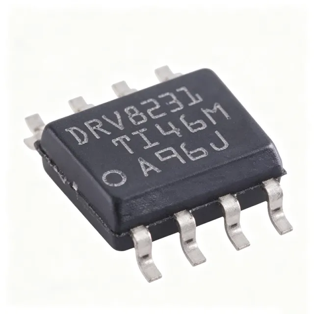
DRV8231 - 35V 3.7A H-Bridge Motor Driver | Texas Instruments
The Texas Instruments DRV8231 is a 35-V, 3.7-A brushed DC motor driver with integrated current regulation, supplied in a compact 8-pin WSON (DSG, 2x2 mm) package. It operates from a 4.5-V to 33-V supply rail and integrates four N-channel MOSFETs forming an H-bridge with a typical RDS(on) of 600 mOhm (including one high-side and one low-side FET). A brushed DC motor driver is a type of motor controller IC that switches power to a DC motor using an H-bridge of transistors, enabling forward, reverse, brake, and coast control. Within the power management IC hierarchy, motor drivers sit between logic-level microcontroller outputs and the power stage, and integrated H-bridge drivers like the DRV8231 combine gate drive, power FETs, charge pump, and protection in a single device. Key features include integrated current regulation with programmable current limit via the ILIM pin, a charge pump that supports 100% duty cycle operation and full N-channel H-bridge efficiency, and low-voltage logic inputs compatible with 3.3-V and 5-V controllers. Two logic inputs (PWM interface on the DRV8231D variant, PH/EN interface on the DRV8231A variant) control the bridge states, minimizing MCU pin usage and firmware complexity. Technically, the DRV8231 family offers pin-to-pin scalable RDS(on) and supply voltage options, allowing designers to support various loads and rails with minimal PCB changes. Integrated protection includes undervoltage lockout, overcurrent protection, and thermal shutdown, reducing external component count and board area compared to discrete MOSFET bridge solutions. Typical applications include brushed DC motor control in printers, small appliances, actuators, robotics, factory automation systems, and consumer electronics, where the compact 2x2 mm WSON-8 package fits space-constrained designs and integrated current regulation protects the motor and PCB traces without an external sense resistor network. When designing with the DRV8231, set the current limit using the ILIM pin resistor per the datasheet equation and provide a solid power ground plane under the exposed pad, since bridge conduction losses scale with the 600 mOhm typical RDS(on) at higher load currents.
DRV8242SQRHLRQ1 - 40V 6A Automotive H-Bridge Driver | Texas Instruments
The Texas Instruments DRV8242SQRHLRQ1 is an automotive-qualified 40V, 6A H-bridge motor driver with integrated high-side current sensing and feedback, housed in a 20-pin VQFN (RHL) package measuring 3.5 x 4.5 x 0.9 mm and rated for operation from -40C to +125C. An H-bridge motor driver is a power management IC that controls the direction, speed, and braking of a DC motor by switching four internal power transistors in complementary pairs. H-bridge drivers sit within the motor driver family of the broader power management IC hierarchy, bridging the gap between low-voltage logic controllers and the inductive loads of brushed DC motors, stepper motors, and actuators used across automotive and industrial systems. Key features include the integrated 40V-rated N-channel H-bridge, an integrated charge pump regulator for high-side gate drive, and on-chip current sensing with regulation that eliminates the need for external sense resistors. Control is provided through PWM or SPI interfaces, and a low-power sleep mode minimizes quiescent current for always-on automotive modules. The DRV8242-Q1 family shares an identical pin function across variants with scalable RON (on-resistance) to match different load currents, allowing designers to scale power capability without PCB redesign. Integrated protection circuitry covers overcurrent, thermal, and supply fault conditions, and the current-proportional output feeds motor current data back to the microcontroller for closed-loop control and diagnostics. Typical applications include automotive brushed DC motor modules such as pumps, fans, actuators, HVAC dampers, seat adjusters, and door latches, as well as industrial motion control where a compact 4.5V to 35V supply range and 6A continuous current are required. When designing with this device, exploit the integrated current-sense regulation to remove external shunt resistors, but ensure the VQFN exposed pad is soldered to an adequate PCB thermal plane to dissipate conduction losses at full 6A load. Verify that the supply path tolerates inductive kick-back beyond the 40V rating during aggressive PWM braking. This page synthesizes verified distributor pricing, drop-in same-family alternatives, and practical design notes not found in the manufacturer datasheet, giving engineers a complete sourcing and design reference for the DRV8242SQRHLRQ1.
DRV8243SQRHLRQ1 - 40V, 12A Automotive H-Bridge Driver | TI
The Texas Instruments DRV8243SQRHLRQ1 is an automotive-grade 40-V, 12-A H-bridge motor driver with integrated current sensing, integrated N-channel power FETs, and SPI-based configurable control, housed in a thermally enhanced VQFN-HR (RHL) power package and qualified to AEC-Q100 for automotive deployment. An H-bridge driver is a power management IC that controls the direction, speed, and braking of DC motors and other inductive loads by switching four bridge arms in controlled combinations. Within the power electronics hierarchy, the DRV8243-Q1 belongs to the integrated motor driver family: a monolithic device combining gate drive, power stage, current sensing, diagnostics, and protection in a single package, eliminating the need for discrete MOSFETs and gate drivers. Key features include a 40 V absolute maximum supply rating supporting 12-V automotive battery systems with load-dump headroom, up to 12 A of current capability from an integrated N-channel H-bridge on a BiCMOS high-power process, and high-side current sensing with regulation plus a current-proportional analog feedback output. The SPI (SQ) control interface allows configuration of off-state diagnostics, current regulation thresholds, slew-rate control, and detailed fault reporting, enabling predictive maintenance and functional-safety architectures. The DRV824x-Q1 family is fabricated on a monolithic BiCMOS high-power process that delivers excellent power handling and thermal performance. The family shares an identical pin function across members with scalable RON, so designers can trade current capability against cost without a PCB respin. A low-power sleep mode minimizes quiescent battery drain, and an integrated charge pump guarantees full enhancement of the high-side N-channel FETs across the supply range. Typical applications include automotive body and comfort functions such as power liftgates, power seats, window lifters, sunroof and pump actuators, as well as industrial 12-V brushed-DC motor drives requiring rich diagnostics. The integrated current-sense amplifier with proportional output removes the external sense resistor in many designs, saving board area and improving efficiency. Design consideration: because the bridge power FETs are integrated, thermal design centers on PCB copper area under the power pad; estimate conduction losses as I^2 x RON per arm and verify junction temperature against the AEC-Q100 Grade 1 ambient range. This page synthesizes distributor pricing, drop-in family alternatives, comparison tables, and practical design notes not found in the manufacturer datasheet.

DRV8256ERGER - 50V 8A H-Bridge Motor Driver with Smart Tune | TI
The Texas Instruments DRV8256ERGER is a 50-V, 8-A H-bridge motor driver with integrated current sense and Smart Tune technology, delivered in a 24-pin VQFN (RGE) package measuring 4x4 mm. It supports bipolar control through PH/EN inputs (no IN1/IN2 PWM pins), integrates two N-channel power MOSFET half-bridges plus low-side current sensing, and operates from a single supply of 4.5 V to 48 V. The device is qualified for -40C to +125C ambient operation and includes comprehensive protection: VM undervoltage lockout, charge-pump undervoltage, overcurrent protection, overtemperature shutdown, and open-load detection. An H-bridge motor driver is a type of brushed DC or stepper motor driver that uses four switching elements arranged in an H topology to drive current in either direction through a single winding. H-bridge drivers belong to the broader family of motor drivers (brushed DC, stepper, BLDC) which in turn fall under power management ICs and discrete semiconductor categories. By integrating the FETs, gate drivers, current sense amplifier, and protection logic in one package, the DRV8256ERGER replaces discrete implementations that would otherwise require dozens of components. Key features include 8-A peak H-bridge output current (derated to ~4.5 A RMS depending on PCB copper area), integrated current sensing that eliminates an external sense resistor, Smart Tune technology that automatically adjusts dead time and decay mode to minimize audible motor noise and current ripple, and a 1.5 A peak gate-drive flyback clamp for inductive loads. The device supports both PWM (PH/EN) and independent half-bridge control modes. The architecture pairs a charge pump (for the high-side gate drive) with a current-shunt monitor on each low-side FET, feeding the integrated sense amplifier whose output appears on the SO pin as an analog voltage. Smart Tune combines four decay modes - slow decay, fast decay, mixed 30%, mixed 60% - and selects them dynamically based on motor current to suppress ripple current and acoustic noise without firmware tuning. Typical applications include brushed DC motors in robotic vacuums, small home appliances, e-bike valve actuators, industrial pumps, and consumer fans. The wide 4.5 V to 48 V supply range covers USB, single-cell Li-ion, lead-acid 12 V, and industrial 24 V / 36 V / 48 V rails. The integrated sense amplifier is particularly valuable in closed-loop torque or current control. When designing with the DRV8256ERGER, place the VM bulk capacitor as close to pins 5-6 and 19-20 (VM/GND) as possible. The exposed thermal pad (pin 24) must be soldered to a top-side copper pour of at least 1 cm^2 to stay within thermal limits at 8 A peak loads. Use 100 nF + 10 uF bypass directly on VM, and add a TVS diode across the motor terminals if the application includes long cable harnesses to absorb flyback transients. This page synthesizes distributor pricing, drop-in pin-compatible alternatives, and practical thermal/PCB layout notes for the DRV8256ERGER that are not consolidated in the TI datasheet alone.
DRV8301DCAR - 65V 3-Phase Gate Driver with Buck Regulator & SPI | Texas Instruments
The Texas Instruments DRV8301DCAR is a 65-V maximum three-phase gate driver with integrated dual current shunt amplifiers, a buck regulator, and an SPI interface, housed in a 56-pin HTSSOP (DCA) package with PowerPAD. It is designed to drive six N-channel power MOSFETs (three half-bridges) for sensored or sensorless brushless DC (BLDC) and permanent-magnet synchronous motor (PMSM) applications. The gate driver section supports a wide 8 V to 60 V motor supply range, while the integrated 1.5 A synchronous buck converter produces an auxiliary 3.3 V or 5 V rail for companion MCUs. A three-phase gate driver is a power-management IC that converts low-power PWM control signals from a microcontroller into the high-current gate-drive signals required by the high-side and low-side MOSFETs of each inverter leg. It sits between the digital control domain (logic-level PWMs) and the high-power motor domain (tens of volts and tens of amps), and is therefore classified within the broader hierarchy of motor drivers > motion controllers > power management ICs > semiconductor. By integrating the gate drive, current sensing, and auxiliary supply, the DRV8301 collapses what would otherwise be three separate ICs into a single device, simplifying BLDC inverter design. Key features include: a programmable 5 mA to 60 mA gate-drive current with adaptive dead-time insertion to prevent shoot-through; integrated dual current-shunt amplifiers with adjustable gain (10/20/40/80 V/V) and 5 µs settling time for FOC torque control; a 1.5 A, 0.8 V to 8.5 V adjustable buck regulator; SPI-configurable protection (overcurrent, overtemperature, undervoltage, gate-drive fault); and an operating temperature range of -40 °C to +125 °C. The HTSSOP-56 PowerPAD package offers θJA ≈ 31 °C/W when the exposed pad is soldered to sufficient copper area. Architecture-wise, the DRV8301 pairs a charge-pump-derived high-side bias supply with a bootstrap-capacitor-per-phase design, allowing 100% duty-cycle operation of the high-side FETs without external floating rails. The current-sense amplifiers use continuous-time chopper-stabilized op-amps to minimize offset drift, which directly improves the low-speed torque accuracy of sensorless FOC schemes. The SPI port allows in-system tuning of dead-time, current-sense gain, OC threshold, and buck VOUT, enabling firmware-controlled optimization for different MOSFET choices. Typical applications include drone (UAV) ESCs, e-bike / e-scooter traction drives, cordless power tools, HVAC fans and pumps, and small industrial servo drives. The DRV8301 is also the gateway IC on TI's well-known DRV8301-69M-KIT reference design for InstaSPIN-FOC motor control. When designing with this part, follow TI's MOSFET short-circuit ruggedness guidance and lay out the PowerPAD with at least 1 in² of 2-oz copper to keep the gate-driver junction within safe limits. This page synthesizes distributor pricing, drop-in alternatives, and application-focused design notes that complement the manufacturer datasheet. The DRV8301DCAR is specified in TI's datasheet revision F, available from ti.com/lit/ds/symlink/drv8301.pdf.
DRV8303DCAR - 65V 3-Phase Gate Driver w/ Dual CSA & SPI | TI
The Texas Instruments DRV8303DCAR is a 65-V maximum three-phase gate driver IC for BLDC and PMSM motor-drive applications, integrating three half-bridge pre-drivers, two current-shunt amplifiers, and an SPI-configurable register set in a 48-pin HTSSOP (DCA) package with PowerPAD. The device delivers up to 1.7-A peak source and 2.3-A peak sink gate-drive current per channel, supporting external N-channel MOSFETs in 6-to-600 V motor systems. A three-phase gate driver, also called a pre-driver or brushless DC motor driver, sits between an MCU/controller and the high-current power stage. It converts low-current PWM logic signals into high-current gate-drive waveforms capable of rapidly switching N-channel MOSFETs in a three-phase bridge, while providing critical protection features (dead-time insertion, bootstrap management, fault reporting) that the controller cannot deliver alone. Within a motor-control system it sits between the microcontroller (such as a C2000 or Sitara) and the three-phase inverter bridge. Key features include a wide 6-V to 60-V single-supply input, integrated bootstrap diodes with trickle-charge support, dual bidirectional current-shunt amplifiers with adjustable gain (5/10/20/40 V/VIA), SPI for configuring gain, dead time, and OC protection thresholds, and a 1.8-V/3.3-V compatible logic interface. Protection features include undervoltage lockout (UVLO) on both the gate-drive and bootstrap rails, overcurrent protection with configurable thresholds, thermal warning and shutdown, and a fault-output flag. The DRV8303 uses a bootstrap gate-driver architecture with an internal charge pump to support 100% duty-cycle PWM, eliminating the need for a separate isolated supply for the high-side drivers. The integrated dual current-shunt amplifiers save board space and BOM by removing the need for external op-amp CSA circuits in sensored and sensorless FOC applications. Typical applications include three-phase BLDC/PMSM motor drives (e.g., drones, e-bikes, robotics, industrial fans, pumps, and CNC spindles), EV traction auxiliaries, and 48-V telecom/server cooling fans. The SPI interface makes it particularly suited to digital motor-control loops using field-oriented control (FOC) or trapezoidal commutation. When designing with this device, choose external N-channel MOSFETs whose total gate charge (Qg) is well below 50 nC to stay within the 1.7-A source / 2.3-A sink envelope, and place the bootstrap capacitors (typically 100 nF ceramic) as close to the BSTx and SHx pins as possible to minimize parasitic inductance. Thermal management: the PowerPAD must be soldered to a sufficient copper area (≥1 in²) to keep junction temperature within the 150 °C shutdown limit at high ambient. This page synthesizes distributor pricing, drop-in alternatives, and practical design notes not found on a typical manufacturer product summary.

DRV8308RHAR - 42V Sensored BLDC Gate Driver with SPI | TI
The Texas Instruments DRV8308RHAR is a 42-V maximum sensored sinusoidal control 3-phase brushless DC (BLDC) gate driver with SPI, housed in a 40-pin VQFN (RHA) 6x6 mm package. It controls sensored BLDC motors with a configurable gate-drive current of 10 mA to 130 mA and operates from 8.5 V to 32 V, with 42-V absolute maximum tolerance on the motor supply rail. What is a BLDC gate driver? A BLDC (brushless DC) gate driver is an integrated circuit that interfaces between a low-power microcontroller and the high-current three-phase inverter that drives a brushless DC motor. The gate driver sits in the power-management hierarchy below the MCU and above the power MOSFETs, providing level shifting, dead-time insertion, gate-drive strength control, and protection features (undervoltage, overcurrent, thermal) so the MCU does not have to handle high-current switching directly. Key features of the DRV8308RHAR include three Hall-sensor inputs for rotor-position feedback, an SPI interface for command and telemetry, configurable gate-drive current from 10 mA to 130 mA per MOSFET, integrated commutation logic, a closed-loop speed controller using CLKIN/FG, and support for both sensored trapezoidal and sensorless (BEMF) commutation. The 40-pin VQFN (RHA) package provides a low-thermal-resistance path for dissipating the gate-drive losses. The architecture combines a precision analog front-end for Hall sensors with a digital speed-control loop and three half-bridge predrivers. The configurable gate-drive current allows the designer to tune switching losses versus EMI for a given power MOSFET. An SPI port enables in-system configuration of current limits, PWM frequency, commutation mode, and read-back of fault status. According to TI product literature, the device is designed for fast closed-loop speed control with minimal MCU overhead. Typical applications include brushless DC fan and pump drives, e-bike and e-scooter traction controllers, cordless power tools, small HVAC blowers, and white-goods appliance motors. The sensored sinusoidal mode produces low acoustic noise and torque ripple, which is critical for fans and pumps used in noise-sensitive environments. When designing with the DRV8308RHAR, ensure the 8.5 V to 32 V motor supply is decoupled with low-ESR ceramic capacitors placed close to the VM and PGND pins. Select external N-channel MOSFETs with Vds ratings comfortably above the maximum motor supply, and program the gate-drive current via SPI to balance switching loss and EMI for the chosen MOSFET package. This page synthesizes current distributor pricing, verified drop-in alternatives, and practical design notes not found in the manufacturer datasheet alone, giving engineers a single source for parametric data, sourcing options, and PCB-layout guidance.
DRV8308RHAT - 42V Sensored BLDC Gate Driver w/ SPI | Texas Instruments
The Texas Instruments DRV8308RHAT is a 42-V max sensored sinusoidal control, 3-phase brushless DC (BLDC) gate driver with SPI, housed in a 40-pin VQFN (RHA) package measuring 6x6 mm. It functions as a pre-driver that controls the gates of six external N-channel MOSFETs with a configurable gate-drive current of 10 mA to 130 mA, enabling optimized switching characteristics across a wide motor-speed range. Motor commutation is driven by Hall sensor inputs, and once a consistent rotor speed is reached the DRV8308 transitions from sensored trapezoidal commutation to sensorless sinusoidal commutation using a single Hall sensor. A brushless DC (BLDC) motor controller is an integrated circuit that sequences power to the three stator windings of a brushless motor in the correct order, converting DC bus voltage into rotating magnetic fields. Within the broader product hierarchy, BLDC motor controllers belong to motor-driver ICs, which are a subset of motion control and ignition ICs within power management. The DRV8308 specifically sits in the gate-driver (pre-driver) category because it does not contain integrated power FETs; instead, it controls external MOSFETs, allowing designers to scale the power stage for higher current motors than integrated-driver ICs can support. Key specifications include an 8.5 V to 32 V (42 V abs max) supply-voltage range, integrated SPI interface for parameter tuning, configurable gate-drive current (10 mA to 130 mA), cycle-by-cycle current limit, and built-in protection including undervoltage lockout, overcurrent protection, and thermal shutdown. The device supports both sensored and sensorless sinusoidal control, enabling smooth low-speed torque and quiet high-speed operation. Hall-sensor inputs are configurable for 60-degree or 120-degree mechanical placement. Typical applications include cordless power tools, e-bikes and electric scooters, drones and multicopter flight controllers, CPU cooling fans, pumps, and small HVAC blowers. The wide 8.5-32 V supply range is compatible with both single-cell Li-ion (with boost) and multi-cell Li-ion packs up to 8S, while the configurable gate drive allows pairing with low-side MOSFETs of various RDS(on) and Qg values to optimize efficiency and EMI for each motor platform. When designing with the DRV8308RHAT, ensure the SPI pull-up resistor on the SDATA line is sized correctly for the selected clock rate, and that the bootstrap capacitors are placed close to the BSTx pins with short traces to minimize switching losses and ringing. The thermal pad of the VQFN-40 must be soldered to a copper pour of at least 1 square inch for reliable operation at sustained high gate-drive currents. This page synthesizes distributor pricing, drop-in alternatives, and practical design notes not found in the manufacturer datasheet, helping engineers select and source the DRV8308RHAT with confidence for BLDC motion-control designs.

DRV8313PWPR - 2.5A Triple 1/2-H Bridge Driver | TI
The Texas Instruments DRV8313PWPR is a triple 1/2-H bridge driver designed for three-phase brushless-DC motors and other loads. It integrates N-channel power MOSFETs in a 1/2-H bridge configuration, providing up to 2.5A continuous output current per channel and 3A peak. The device operates from a supply voltage range of 8V to 60V, making it suitable for a wide range of industrial and consumer applications. Housed in a 28-pin HTSSOP (PWP) package, the DRV8313PWPR offers a compact solution for motor control. A motor driver is an integrated circuit that translates low-power control signals from a microcontroller into the higher voltage and current needed to drive a motor. The DRV8313PWPR is a triple 1/2-H bridge driver, meaning it contains three independent half-bridge outputs, each capable of sourcing or sinking current. This configuration is ideal for driving three-phase brushless-DC motors, where each phase is connected to one half-bridge. The device also supports independent control of each half-bridge, allowing it to drive solenoids, relays, or other loads. Key features of the DRV8313PWPR include a wide operating voltage range of 8V to 60V, low on-resistance MOSFETs for high efficiency, and overcurrent, overtemperature, and undervoltage lockout protection. The device also features a low-power sleep mode to reduce quiescent current when the motor is not running. These features make it a robust choice for demanding motor control applications. The DRV8313PWPR uses a simple PWM interface, allowing direct connection to a microcontroller's PWM outputs. Each half-bridge can be controlled independently, enabling flexible motor control schemes such as trapezoidal or sinusoidal commutation. The device also includes a current-sense output that can be used for closed-loop current control, enhancing system performance. Typical applications include three-phase brushless-DC motor drives for fans, pumps, and robotics, as well as solenoid drivers and other inductive loads. The wide voltage range and high current capability make it suitable for both 12V and 24V systems, common in industrial and automotive environments. When designing with the DRV8313PWPR, ensure adequate PCB copper area for heat dissipation, especially at high currents. The exposed thermal pad should be soldered to a large ground plane to improve thermal performance. Additionally, place decoupling capacitors close to the power supply pins to minimize voltage transients.

DRV8323RSRGZR - 65V 3-Phase Smart Gate Driver with Buck Regulator | Texas Instruments
The Texas Instruments DRV8323RSRGZR is a 65-V maximum three-phase smart gate driver with integrated buck regulator, three current-shunt amplifiers, and an SPI interface, housed in a 48-pin VQFN (RGZ) 7x7 mm package with an operating range of 6 V to 60 V on the motor supply. What is a three-phase smart gate driver? In motor drive systems a three-phase smart gate driver is a power-management IC that sits between a low-power MCU/controller and the high-current N-channel power MOSFETs that commutate a three-phase brushless DC (BLDC) or permanent-magnet synchronous motor (PMSM). It provides level shifting, gate-drive current, fault protection, and current sensing, replacing dozens of discrete components and shrinking the inverter stage to a single chip. Within the broader taxonomy: gate driver -> motor driver -> power management IC -> semiconductor. Key features include a wide 6 V to 60 V operating range (suitable for 12 V, 24 V and 48 V industrial buses), integrated 3.3 V3/3 LDO for MCU supply, integrated 0.7 A buck regulator, three integrated current-shunt amplifiers supporting low-side or in-line sensing, integrated SPI for configuration and fault telemetry, and programmable gate-drive current up to 1 A peak source / 2 A sink with adjustable dead time and slew-rate control. Protection features include VM undervoltage lockout, VCP charge-pump undervoltage, gate-drive fault, overcurrent (OCP), overtemperature (OTSD), and motor-locked detection with fault pin indication. The DRV8323R architecture combines a smart gate driver (DRV8323 base) with an integrated buck converter and three dedicated current-sense amplifiers, eliminating the need for external op-amps and DC-DC converters that traditionally accompany three-phase FET bridges. The internal charge pump supports 100% duty-cycle high-side drive, while the SPI bus exposes 16 configuration and 12 status registers for diagnostics, making it suited to FOC, trapezoidal and sinusoidal commutation schemes. The 48-pin QFN package offers a low-inductance ground reference and Power-PowerPAD thermal pad for high-current operation. Typical applications include cordless power tools, e-bikes and e-scooters, drones and UAVs (multirotor ESCs), automated guided vehicles (AGVs), robotic vacuum cleaners, white goods (washing machines, refrigerators with BLDC compressors), industrial fans and pumps, and 48 V server fans. The wide VIN range and integrated buck make it ideal for battery-powered tools where multiple rails must be generated from a single pack. When designing with the DRV8323RSRGZR, follow the datasheet layout guidelines: place the three bootstrap capacitors (CBST) as close as possible to the BST_X and OUT_X pins, and use a low-ESR 1 A ceramic on VM and VCP. Use a 4-layer PCB with a continuous ground pour stitched around the RGZ package to handle the gate-driver switching transients. This page synthesizes distributor pricing, drop-in alternatives, and practical design notes not found in the manufacturer datasheet, including a side-by-side comparison versus the DRV8320, DRV8353, and DRV8313 families.
DRV8343SPHPRQ1 - Automotive 3-Phase Smart Gate Driver | TI
The Texas Instruments DRV8343SPHPRQ1 is an automotive-grade, three-phase smart gate driver for 12-V to 24-V battery systems, integrating three half-bridge gate drivers and three current-sense amplifiers in a 48-pin HTQFP (7x7 mm) PowerPAD package. It provides 5.5 V to 60 V operating range, supports N-channel MOSFET half-bridges, and includes an SPI interface for fault monitoring and configuration, plus independent source/drain pins enabling solenoid-style control. A gate driver IC is a power-management device that sits between a low-power MCU/controller and the high-current N-channel MOSFETs of an inverter. The DRV8343-Q1 family is a "smart" gate driver: it integrates gate-drive buffers, charge-pump and bootstrap supplies, current-shunt amplifiers, and protection logic. It belongs to the broader hierarchy of motor driver IC -> three-phase gate driver -> brushless DC (BLDC) and permanent-magnet synchronous motor (PMSM) inverter -> power management -> semiconductor IC. Key features include three integrated current-shunt amplifiers with programmable gain (via SPI), 1-A peak gate-drive current, integrated charge-pump and bootstrap for 100% duty-cycle high-side drive, independent high-side/low-side control for solenoid applications, and comprehensive protection: VDS overcurrent, VGS fault, undervoltage, thermal warning, and thermal shutdown. The DRV8343SPHPRQ1 (SPI variant) gives designers real-time fault telemetry and configurable parameters versus the H/W variant. Architecturally, the device pairs a charge pump for the high-side floating rails with a linear regulator for the low-side gate supply, plus three low-offset op-amps sized for current-sense shunts. This integration reduces BOM count versus discrete solutions, improving automotive inverter reliability and shrinking PCB area for under-hood motor control. Typical applications include 12-V/24-V automotive three-phase BLDC and PMSM motors such as electric water pumps, oil pumps, HVAC blowers, e-compressors for electric-vehicle HVAC, electric power steering (EPS) auxiliary drives, traction auxiliaries, and traction inverters up to several kW. When designing with the DRV8343-Q1, follow datasheet MOSFET selection guidance, place the shunt resistors near the SP/SN pins to minimize Kelvin-loop error, and add a thermal pad with adequate copper to keep junction temperature below the 150 C shutdown threshold. This page synthesizes distributor pricing, AEC-Q100 qualified drop-in alternatives (same 48-HTQFP footprint), and practical layout guidance not found in the manufacturer datasheet alone.

DRV8350FHRTVR - 102V 3-Phase Smart Gate Driver | Texas Instruments
The Texas Instruments DRV8350FHRTVR is a 102-V maximum three-phase Functional Safety Quality-Managed smart gate driver for brushless DC (BLDC) motor applications, integrating three half-bridge MOSFET drivers in a 32-pin WQFN (5x5 mm) package. Headline parameters include a 102-V abs-max supply rating, integrated 250-mA/750-mA adjustable gate-drive current settings, and hardware-interface (HW) variant SPI-less control with a 5x5-mm WQFN RTV footprint. The device drives six external N-channel MOSFETs configured as three half-bridges, supporting 1-PWM, 3-PWM, and 6-PWM commutation modes. What is a smart gate driver? A smart gate driver is an integrated circuit that sits between a microcontroller's low-voltage PWM outputs and the high-power N-channel MOSFETs of a motor inverter. By embedding level shifting, dead-time generation, gate-drive current regulation, and protection (overcurrent, overtemperature, undervoltage, and short-circuit), the smart gate driver replaces dozens of discrete components and reduces PCB area while improving reliability. The DRV8350F belongs to the broader category of three-phase motor drivers, which sit between microcontrollers and motor windings in the BLDC system hierarchy: MCU -> gate driver -> power MOSFETs -> BLDC motor. Key features include integrated charge-pump and bootstrap supply for 100% duty-cycle high-side drive, a programmable dead time, and a 75-V wide common-mode CSA (current shunt amplifier) with adjustable gain. The hardware variant eliminates SPI register access, simplifying firmware and reducing MCU overhead. Functional Safety Quality-Managed documentation includes failure modes, effects, and diagnostics analysis (FMEDA) and a safety manual, which is uncommon for gate drivers and valuable for IEC 61508 / ISO 26262 development. Architecture combines a charge-pump regulator (for low supply conditions), three bootstrap diodes, three low-side gate drivers, three high-side gate drivers, and an integrated current-shunt amplifier. The DRV8350FHRTVR is the "F" Functional Safety variant of the DRV835x family, which also includes the DRV8350 (non-functional-safety) and DRV8353 (with integrated buck regulator) derivatives. Typical applications include cordless power tools, e-bikes, e-scooters, drones, robotics, small pumps, and fans where 100-V absolute-max ratings and 3-phase brushless drive are required. The HW interface makes it well-suited for cost-sensitive designs without SPI firmware overhead. Choose this part when you need a 100-V class three-phase gate driver with functional-safety collateral but without an integrated buck. When designing with the DRV8350FHRTVR, ensure the SHx pins have local 0.1-uF + bootstrap-capacitor ceramic bypass and that the GVDD regulator cap is sized per datasheet for 4.7 uF or larger. The CSA inputs must be biased so that 0-A current sits near mid-supply to maximize linear input range.
DRV8350HRTVR - 102V 3-Phase Smart Gate Driver | Texas Instruments
The Texas Instruments DRV8350HRTVR is a 102-V maximum three-phase smart gate driver for brushless DC (BLDC) motor applications, housed in a 32-pin WQFN (RTV) package measuring 5x5 mm. It integrates three half-bridge gate drivers capable of sourcing 1 A and sinking 2 A peak gate current, with a wide 6-V to 95-V operating supply range and integrated bootstrap, charge pump, and dual LDO architecture for high-side/low-side gate drive. The part operates from -40C to +125C junction temperature, making it suitable for industrial automation, e-mobility, and white-goods environments. What is a three-phase smart gate driver? A smart gate driver is an integrated circuit that sits between a microcontroller (MCU) and the discrete power MOSFETs (or GaN/IGBTs) of a three-phase inverter. It level-shifts low-voltage PWM signals to the high-side gate drive supply, provides strong gate sourcing/sinking currents for fast switching, and typically includes protection features such as undervoltage lockout, dead-time insertion, and shoot-through prevention. Smart gate drivers are a sub-category of motor driver ICs, which themselves fall under the broader power management and motion control semiconductor taxonomy. Key features include a hardware (HW) interface variant (no SPI), integrated 3-phase charge pump for 100% duty-cycle support, adjustable dead time, and protection functions including VDS overcurrent sensing (via external shunt), gate-drive undervoltage lockout (UVLO), and thermal shutdown. The integrated dual LDO (5 V and 3.3 V) supplies the MCU and housekeeping circuits without external regulators, simplifying BOM. The hardware interface uses six PWM inputs (3x high-side, 3x low-side) plus enable and fault flags. Typical applications include field-oriented control (FOC) of BLDC/PMSM motors in e-bikes, drones, cordless tools, and small industrial pumps; sinusoidal current control of appliance motors; and trapezoidal commutation of ceiling fans and pumps. The DRV8350H variant is preferred when the design MCU already performs current control and only needs gate-drive and protection, eliminating SPI register overhead. Design considerations include thermal management: at 1 A continuous gate current and high switching losses, the 32-pin WQFN EP package requires an exposed thermal pad with substantial copper pour. This page synthesizes distributor pricing, drop-in alternatives, and practical design notes not found in the manufacturer datasheet.
DRV8350RSRGZT - 102V 3-Phase Smart Gate Driver with Buck Regulator | Texas Instruments
The Texas Instruments DRV8350RSRGZT is a 102-V maximum, 3-phase smart gate driver for brushless DC (BLDC) motor applications, integrating an optional buck regulator and triple low-side current-shunt amplifiers in a 48-pin VQFN (RGZ) 7x7 mm package with exposed thermal pad. Operating across 9-V to 100-V supplies, the device drives three external N-channel MOSFET half-bridges and supports SPI-based configuration of slew rate, current-shunt gain, and protection thresholds. A gate driver is a power-electronics IC that accepts low-power logic-level PWM commands and translates them into the high-current gate-drive signals required to switch MOSFETs or IGBTs in a half-bridge. The DRV8350 sits in the 'smart gate driver' category, which adds integrated current sensing, adjustable drive strength, and on-chip protection. Its parent taxonomy extends from gate driver to motor driver to motor control IC to power management semiconductor. Key features include a smart gate-drive architecture with adjustable 1.5 A / 0.5 A / 0.25 A source/sink current settings for EMI tuning, VGS handshake circuitry that prevents simultaneous half-bridge conduction (shoot-through), integrated triple low-side current-shunt amplifiers with programmable gain, an internal 3.3-V/5-V selectable buck regulator for auxiliary rails, and comprehensive protection including VM undervoltage lockout, gate-drive over-voltage, and thermal shutdown. The VQFN-48 (RGZ) 7x7 mm package provides low RDS(on) thermal paths. The DRV8350 is built on TI's 100-V BCD process, supporting switching frequencies up to 200 kHz per phase and providing TTL-compatible inputs that interface directly with 3.3-V or 5-V MCUs such as C2000 or Sitara. The integrated current-shunt amplifiers eliminate external op-amps, while the SPI interface enables per-channel diagnostics for safety-critical systems. Typical applications include 3-phase brushless DC motor control in industrial fans, pumps, and e-bikes; cordless power tools; 48-V e-mobility; servo drives; and robotic actuators. The wide 9-V to 100-V input also supports solar pump inverters and 24-V/36-V/48-V battery-powered traction. When designing with this device, ensure that the bootstrap capacitors on each half-bridge are sized for the worst-case PWM duty cycle and that sufficient bulk capacitance is placed at VM. TI's SLAA851 application note provides detailed bootstrap-capacitor sizing guidance and recommended MOSFET selections.
DRV8350SRTVR - 102V 3-Phase Smart Gate Driver | Texas Instruments
The Texas Instruments DRV8350SRTVR is a 102-V maximum three-phase smart gate driver for brushless DC (BLDC) motor applications, integrating three half-bridge gate drivers plus a SPI-configurable block in a 32-pin WQFN (RTV) package with 5x5 mm body. Headline parameters include a 102-V abs-max VM rating, 6-V to 95-V recommended VM operating range, integrated 3.3-V LDO, programmable slew rate, and SPI for current shunt amplifier, OCP, and dead-time configuration. The device targets 1.5-A to 5-A peak motor phase current when used with suitably rated external power MOSFETs. A three-phase smart gate driver is a mixed-signal IC that sits between a microcontroller/MCU and the three half-bridges of external N-channel power MOSFETs in a BLDC/PMSM inverter stage. It accepts six low-power PWM control inputs (or one to three PWMs with commutation) and produces gate-drive signals capable of switching the high-side FETs with a bootstrap supply and the low-side FETs with VGS drive from VM. As part of the power management hierarchy, it sits between the gate driver family and the broader class of motor driver and motion control ICs, providing the analog/digital interface between low-voltage logic and high-current power conversion. Key differentiating features include integrated charge-pump ready architecture for 100% duty-cycle high-side drive, three integrated current-shunt amplifiers (CSA) with adjustable gain and bidirectional support, programmable dead time (0.05 ns to 4 us depending on configuration), and comprehensive fault protection: VMOT undervoltage, VDS overcurrent on each FET, gate-driver fault, thermal warning/shutdown, and charge-pump undervoltage. The SPI variants (DRV8350S) also expose registers for fine tuning of CSA gain, OCP threshold, blanking time, and dV/dt control via the gate-drive current bits. Typical applications include field-oriented control (FOC) BLDC/PMSM motors in e-bikes, drones, cordless power tools, pumps, fans, and small HVAC blowers, as well as industrial servo drives in the 24-V to 80-V bus range. The integrated CSAs reduce BOM count versus discrete op-amp solutions and the wide VM range supports battery packs from 6S Li-ion (25.2V max) to industrial 48-V to 72-V systems. The device is pin-compatible with the DRV8353, DRV8353S, and DRV8323RS in the same WQFN-32 footprint, simplifying platform design across product tiers. When designing with the DRV8350SRTVR, ensure the VM decoupling (4.7 uF X7R minimum per VM pin) and the VDRAIN/CP bootstrap network is per the datasheet. Verify thermal performance with worst-case VM and switching loss; the WQFN-32 (RTV) package exposes a thermal pad that must be soldered to a sufficiently large copper pour. Use the SPI to log fault registers in production for field diagnostics.