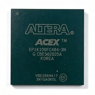
A54SX72A-FGG484 - 108K Gate Antifuse FPGA 484-FBGA | Microchip
料号: A54SX72A-FGG484 ✓ 量产中| 数量 | 单价 | 小计 |
|---|---|---|
| 1 | $165 | $165.00 |
| 10 | $152.4 | $1,524.00 |
| 100 | $138.75 | $13,875.00 |
| 500 | $127.9 | $63,950.00 |
| 1,000 | $118.6 | $118,600.00 |
A54SX72A-FGG484 概述
A field-programmable gate array (FPGA) is a semiconductor device containing a fabric of configurable logic blocks and programmable interconnects that designers configure after manufacturing. Within the programmable logic hierarchy, the FPGA sits above SPLDs and CPLDs as the highest-capacity category of programmable logic IC. The SX-A family from Actel (now Microchip, formerly Microsemi) uses antifuse programming technology, in which permanent one-time-programmable connections are formed during programming.
Key differentiating features include the antifuse fabric that yields near-ASIC routing delays, high resistance to configuration readback (providing inherent design security), zero standby configuration-loading time at power-up, and low static power consumption. With a toggle rate of up to 217 MHz on a 0.25um/0.22um CMOS process, the device supports high-throughput glue logic, bus bridging, and state-machine integration while replacing multiple discrete devices with a single-chip solution.
Architecturally, each SX-A logic module combines combinational and sequential elements, and the A54SX72A is the largest member of the family, offering multiple global and quadrant clock networks (CLKA, CLKB, and QCLK resources) per Microchip documentation for low-skew clock distribution. The FBGA package provides short, low-inductance ball connections suited to high-speed signal integrity.
Typical applications include industrial control and automation, communications and networking line cards, avionics and defense systems requiring one-time-programmable security, medical instrumentation, and test equipment backplanes where instant-on operation and configuration tamper resistance matter.
When designing with this device, plan I/O banking and 2.5V supply distribution early, and use Microchip Libero SoC design tools with the SX-A macro libraries; note that antifuse programming is irreversible, so verify the design fully in simulation before programming production units.
This page synthesizes distributor pricing tiers, drop-in alternatives within the same 484-ball FBGA footprint, and practical design notes not found in the manufacturer datasheet.
直接替换替代料: A54SX72A-FGG484 ——相同封装,引脚兼容。需要 PCB 改动的不同封装料号已排除。
本系列中的变体
可与以下型号直接替换的同系列型号: A54SX72A-FGG484 (相同外形与封装尺寸) ——差异在于 Package, RoHS Status, Speed Grade, Operating Temperature, System Gates.
快速对比工具——选择替代料号进行并排对比:
A54SX72A-FGG484A
✅ 直接替换✓ 有现货
联系询价
查看数据手册 →A54SX72A-2FGG484
✅ 直接替换✓ 有现货
$85.6 / 个
查看数据手册 →A54SX72A-1FGG484I
✅ 直接替换✓ 有现货
$225 / 个
查看数据手册 →A54SX72A-FFGG484
✅ 直接替换✓ 有现货
联系询价
查看数据手册 →A54SX72A-FGG484M
✅ 直接替换✓ 有现货
$2920.69 / 个
查看数据手册 →A54SX72A-1FGG484M
✅ 直接替换✓ 有现货
$73.4 / 个
查看数据手册 →A54SX72A-FGG484 最大额定值与电气特性
| Family | SX-A (Antifuse FPGA) |
| System Gates | 108000 |
| Typical Usable Gates | 72000 |
| Configurable Logic Blocks (CLBs) | 6036 |
| Logic Cells | 4024 |
| User I/O | 360 |
| Maximum Toggle Frequency | 217 MHz |
| Core Supply Voltage | 2.5 V |
| Maximum Supply Voltage | 2.75 V |
| Process Technology | 0.25 um / 0.22 um CMOS |
| Programming Technology | Antifuse (one-time programmable) |
| 封装 | 484-ball FBGA |
| 安装类型 | Surface Mount |
| 工作温度 | -40C to +125C |
| Clock Resources | CLKA, CLKB, QCLK (global and quadrant clocks) |
| Speed Grade | Standard (per MPN suffix) |
| Configuration | Instant-on, no external configuration memory required |
A54SX72A-FGG484 484-ball fbga 引脚配置指南
A54SX72A-FGG484(484-ball fbga 封装)的引脚配置。 该数字 IC 包含 GPIO、通信接口(UART、SPI、I2C)和电源引脚。请参阅制造商数据手册以了解复用引脚功能和配置选项。对嵌入式系统设计和 PCB 布局至关重要。

暂无详细引脚数据: A54SX72A-FGG484.
请参阅 数据手册 以查看完整引脚配置。
典型应用
A54SX72A-FGG484 适用于 6 应用s: Industrial Control and Automation, Avionics and Defense Systems, Communications and Networking Line Cards, Test and Measurement Equipment, Medical Instrumentation, Secure Embedded Control and Single-Chip Integration.
Industrial Control and Automation
The A54SX72A-FGG484 integrates PLC I/O logic, motor-control sequencing, and bus-interface glue logic into a single 108K-gate antifuse device, replacing multiple discrete ASSPs and reducing BOM count. Its instant-on configuration means machinery control logic is active the moment 2.5V power is applied, with no boot delay from configuration memory - important for safety interlock circuits that must assert outputs at power-up. The 360 user I/O in the 484-ball FBGA provide enough parallel I/O to bridge fieldbus transceivers, encoders, and sensor banks directly, while the 217 MHz class fabric performance handles deterministic state machines. Because the antifuse configuration is permanent and non-readable, control IP is protected on the factory floor.
推荐
Avionics and Defense Systems
Antifuse FPGAs are a mainstay in avionics and defense processing cards because routing and configuration are programmed once and cannot be altered or read back, giving inherent protection against configuration tampering and SEU-driven routing corruption. The A54SX72A-FGG484 provides 72,000 typical gates for bus arbitration, MIL-STD-1553 and ARINC-interface glue logic, and radar pre-processing pipelines, in a 484-ball FBGA suited to conduction-cooled board stacks. The military-grade A54SX72A-FGG484M shares the same footprint for extended-environment programs. Instant-on operation supportssystems that must be functional within milliseconds of power application, and low static power suits convection-limited or battery-backed platforms.
推荐
Communications and Networking Line Cards
On telecom and datacom line cards, the A54SX72A-FGG484 performs backplane bus bridging, framer-to-PHY glue logic, and packet framing at line rates enabled by its 217 MHz class fabric. The 360 user I/O of the 484-ball FBGA allow a single device to terminate multiple parallel bus segments, and the quadrant clock networks (CLKA, CLKB, QCLK) provide low-skick clocking per Microchip application guidance for the A54SX72A. Antifuse configuration means the card is forwarding traffic immediately at power-up with no configuration download, reducing link-recovery time, while the fixed programmed interconnect delivers deterministic, repeatable timing that does not vary after programming - valuable for multi-card timing margin budgeting.
推荐
Test and Measurement Equipment
Bench instruments, ATE boards, and protocol analyzers benefit from the A54SX72A-FGG484's combination of 4024 logic cells for pattern generation and comparison engines, plus 360 user I/O for driving wide parallel test buses from a single device. The 484-ball FBGA offers short, low-inductance ball connections that preserve signal integrity on high-speed stimulus paths. Because configuration is one-time-programmed, an instrument's digital subsystem powers up in its final state immediately - no configuration latency during calibration sequences - and the design cannot drift between units. Timing-closed against the appropriate speed grade, the fabric sustains the 217 MHz class operation needed for state-machine-based test sequencing and edge detection.
推荐
Medical Instrumentation
Diagnostic imaging subsystems, patient-monitoring front ends, and laboratory analyzers use the A54SX72A-FGG484 as the digital hub that sequences acquisition chips, aggregates sample streams, and manages interface logic on a single 108K-gate die. Deterministic antifuse interconnect supports repeatable timing for safety-related control paths, and instant-on configuration ensures monitoring logic is live as soon as power is present, which matters for devices with fast power-up-to-patient-ready requirements. The 2.5V core keeps static power low inside enclosure-constrained instruments, and the design security of one-time programming protects proprietary algorithms embedded in the control fabric from extraction or cloning across the production fleet.
推荐
Secure Embedded Control and Single-Chip Integration
For OEM products where firmware-equivalent design IP must not be extracted, the A54SX72A-FGG484 offers a configuration fabric that is programmed once via antifuse and provides no readback path - a security posture SRAM FPGAs cannot match without additional encryption silicon. The 72,000 typical gates let designers integrate microprocessor glue logic, bus masters, security comparators, and boot sequencing into one chip, cutting BOM count and eliminating external configuration flash, which is itself an attack surface. Instant-on operation removes cold-boot delays in secure systems that must enforce policy from the first clock cycle. The 484-ball FBGA footprint also scales across the Microchip SX-A speed and temperature grades for cost and environment tuning.
推荐
推荐产品汇总
工程参考数据: A54SX72A-FGG484 ——对比、设计指导和合规信息。
选型指南
与替代料对比
| 参数 | 本产品 | A54SX72A-FGG484A | A54SX72A-2FGG484 | A54SX72A-1FGG484 | A54SX72A-FGG484M |
|---|---|---|---|---|---|
| Package | 484-ball FBGA | 484-ball FBGA - same | 484-ball FBGA - same | 484-ball FBGA - same | 484-ball FBGA - same |
| Brand | Microchip Technology | Microchip Technology | Microchip Technology | Microchip Technology | Microchip Technology |
| System Gates | 108000 | 108000 | 108000 | 108000 | 108000 |
| User I/O | 360 | 360 | 360 | 360 | 360 |
| Core Supply Voltage | 2.5 V | 2.5 V | 2.5 V | 2.5 V | 2.5 V |
| Programming Technology | Antifuse (OTP) | Antifuse (OTP) | Antifuse (OTP) | Antifuse (OTP) | Antifuse (OTP) |
关键差异点
- Instant-on, configuration-free operation (对比 SRAM FPGAs (Xilinx/Altera equivalents))
- Design security via non-readable configuration (对比 A54SX72A-FG256 (smaller package variant))
- Higher timing headroom option at same footprint (对比 A54SX72A-FGG484A)
- Trade-off: lower fabric density than modern FPGAs (对比 Actel AX500-FGG484)
设计说明
The A54SX72A-FGG484 operates from a 2.5V core with a 2.75V absolute maximum. Use a dedicated low-noise LDO or buck regulator with tight tolerance for the core rail, and decouple each VCC/VCCA ball pair with 0.1uF ceramic capacitors placed on the underside of the FBGA footprint. Power-up sequencing per the SX-A datasheet must be observed; antifuse devices are instantly active, so a dirty ramping rail can cause I/O glitching at boot. Verify total supply current against your design's resource utilization using Libero power estimation before fixing the regulator budget.
The 484-ball FBGA provides short ball interconnects with low parasitic inductance, but with 360 user I/O switching, simultaneous switching noise (SSN) becomes the dominant constraint. Distribute ground balls between high-toggle I/O groups, keep return paths continuous under breakout fanout, and series-terminate long point-to-point nets (22-33 ohm typical). Clock distribution should use the dedicated CLKA, CLKB, and QCLK quadrant clock resources per Microchip application notes, rather than general fabric routing, to hold skew within the datasheet timing budget.
The most costly mistake with this device is treating it like a reprogrammable FPGA: antifuse programming is one-time and irreversible. Complete functional simulation, timing closure against the correct speed-grade table, and design review before programming any unit. Also confirm the speed grade suffix at purchase - designs closed on the standard part can use -1, -2, or A grades, but the reverse substitution can fail timing. Finally, verify the 484-ball footprint against the official SX-A datasheet ballout, not a derived land pattern from another package variant.
合规信息
Compliance status not stated in the provided web data; confirm RoHS/REACH status on the Microchip product page for the specific ordering code.