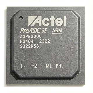
A54SX72A-FGG484A - 108K-Gate Antifuse FPGA, 484 FBGA | Microchip
MPN: A54SX72A-FGG484A ✓ Active| Qty | Unit Price | Extended |
|---|---|---|
| 1 | $0 | $0.00 |
| 10 | $0 | $0.00 |
| 100 | $0 | $0.00 |
| 500 | $0 | $0.00 |
| 1,000 | $0 | $0.00 |
A54SX72A-FGG484A Overview
A field-programmable gate array (FPGA) is a semiconductor device containing configurable logic blocks and programmable interconnects that engineers program after manufacturing. Within the FPGA hierarchy, the SX-A family belongs to the antifuse (one-time programmable, OTP) class of FPGAs, sitting alongside SRAM-based and flash-based FPGA types in the broader programmable logic and power/logic integration landscape. Antifuse FPGAs configure their interconnect permanently at power-up programming, which gives them inherent security and low static power advantages over SRAM FPGAs.
Key features of the A54SX72A include 108,000 equivalent system gates with 72,000 typical gates available, 360 configurable user I/O, and single-chip integration of multiple logic functions to reduce system cost. Because the configuration is stored in antifuse elements, no external configuration PROM or boot flash is required, and the bitstream is never exposed on the bus, providing design security that SRAM FPGAs cannot match. The device operates from a 2.5 V supply and is fabricated on a 0.25 um CMOS process, supporting clock rates up to 217 MHz.
Architecturally, the SX-A device provides a sea-of-modules fabric of combinatorial and sequential logic modules (C-cells and R-cells) interconnected through a programmed routing network, with dedicated global and quadrant clock networks (CLKA, CLKB, and QCLK) for low-skew clock distribution across the die, as documented in the SX-A family datasheet.
Typical applications include industrial control and automation logic integration, communications and networking line-card glue logic, aerospace and defense systems where design protection matters, and legacy system re-design or obsolescence bridging where a one-time-programmable, secure FPGA replaces multiple ASSPs.
A key design consideration is that antifuse devices are one-time programmable: unlike SRAM FPGAs, there is no in-system reconfiguration, so design verification must be complete before programming, and spare gates should be reserved for ECOs.
This page consolidates verified distributor listings, drop-in same-family alternatives, and practical design notes not found in the manufacturer datasheet, providing buyers and engineers with a single decision-ready reference.
Drop-in alternatives for A54SX72A-FGG484A — same package, pin-to-pin compatible. Different-package parts requiring PCB rework are excluded.
Variants in this series
Same-series models that are drop-in compatible with A54SX72A-FGG484A (same form factor and footprint) — differing in RoHS Status, Package, Operating Temperature, System Gates, Speed Grade.
Quick Comparison Tool — Select alternative parts for side-by-side comparison:
A54SX72A-FFGG484
✅ Drop-In✓ In Stock
Contact for price
View Datasheet →A54SX72A-FGG484M
✅ Drop-In✓ In Stock
$2920.69 / Unit
View Datasheet →A54SX72A-1FGG484I
✅ Drop-In✓ In Stock
$225 / Unit
View Datasheet →A54SX72A-2FGG484I
✅ Drop-In✓ In Stock
$112 / Unit
View Datasheet →A54SX72A-FGG484M
✅ Drop-In✓ In Stock
$2920.69 / Unit
View Datasheet →A54SX72A-FG484I
✅ Drop-In✓ In Stock
$217.72 / Unit
View Datasheet →A54SX72A-FGG484A Maximum Ratings & Electrical Characteristics
| Family | SX-A (antifuse FPGA) |
| System Gates | 108,000 (72,000 typical gates) |
| User I/O | 360 |
| Core Supply Voltage | 2.5 V |
| Maximum System Frequency | 217 MHz |
| Process Technology | 0.25 um CMOS |
| Programmability Type | Antifuse (one-time programmable, OTP) |
| Package | 484-ball FBGA (FGG484) |
| Mounting Type | Surface Mount |
| Speed Grade | Standard (-A) |
| Lead Free | Yes (per distributor listings) |
| External Configuration Device | Not required (non-volatile antifuse) |
| Clock Networks | CLKA, CLKB, quadrant clocks (QCLK) |
| RoHS Status | Compliant (lead-free suffix G per Microchip convention) |
A54SX72A-FGG484A 484-ball fbga (fgg484) Pin Configuration Guide
Pin configuration for A54SX72A-FGG484A (484-ball fbga (fgg484) package). This digital IC includes GPIO, communication interfaces (UART, SPI, I2C), and power pins. Refer to the manufacturer datasheet for alternate pin functions and configuration options. Essential for embedded system design and PCB layout.

No detailed pinout data available for A54SX72A-FGG484A.
Refer to the datasheet for full pin configuration.
Typical Applications
A54SX72A-FGG484A is suitable for 6 applications: Industrial Control and Automation, Aerospace and Defense Secure Logic, Communications Line-Card Glue Logic, Legacy System Redesign and Obsolescence Bridging, Anti-Cloning and IP Protection Designs, Medical Device Control Logic.
Industrial Control and Automation
The A54SX72A-FGG484A consolidates glue logic, interface bridging, and sequencing functions that would otherwise require multiple ASSPs and PLDs on industrial control boards. Its 108,000 system gates and 360 user I/O give enough capacity to absorb address decoding, bus arbitration, and motor-control interfaces on a single 2.5 V-core device, while the antifuse configuration is immune to configuration upsets from the noisy electrical environment typical of factory automation. Because no configuration PROM is needed, board BOM cost and boot time are reduced, and the instant-on behavior supports safety-relevant I/O that must be valid at power application. Designers should budget the 0.25 um process timing at up to 217 MHz and reserve quadrant clock resources (CLKA, CLKB, QCLK) for low-skew distribution to distributed I/O registers across the FBGA-484 ball field.
Recommended
Aerospace and Defense Secure Logic
Antifuse FPGAs are favored in defense electronics because the programmed interconnect is permanent and the design bitstream never appears on an external bus, eliminating the configuration-readback attack surface inherent to SRAM FPGAs. The A54SX72A-FGG484A's 108K system gates implement secure boot logic, cryptographic glue functions, or bus protocol bridges, while the non-volatile antifuse configuration removes the system-level dependency on external flash that radiation and tamper considerations make undesirable. The military-screened sibling A54SX72A-FGG484M shares the identical 484-ball FBGA footprint, enabling a common PCB across commercial and screened build levels. Designers must accept the one-time-programmability constraint: hardware design freeze must precede programming, so flight programs typically hold blank-device inventory for engineering iterations before committing flight lot programming.
Recommended
Communications Line-Card Glue Logic
Telecom and datacom line cards frequently need a flexible logic element to marry legacy backplane interfaces (TDM buses, HDLC framers, crossbar control) to modern PHYs. The A54SX72A-FGG484A serves this role with 360 I/O - sufficient for wide parallel backplane buses - and 217 MHz internal performance for protocol state machines running from the CLKA/CLKB global clocks. The single-chip integration claim on the Microchip product page translates directly here: functions previously spread across CPLDs, decoders, and registers collapse into one 484-ball FBGA, shrinking board area and power. Because the antifuse configuration is fixed at manufacture, line-card revisions require device replacement rather than reflashing; production programs typically pair this device with boundary-scan test coverage to verify connectivity after assembly, since internal logic cannot be re-read after antifuse programming.
Recommended
Legacy System Redesign and Obsolescence Bridging
When EOL ASSPs, gate arrays, or older CPLDs disappear from the market, the A54SX72A-FGG484A provides an obsolescence bridge: its 108K-gate capacity absorbs reverse-engineered legacy logic, and the antifuse family's stability (documented since the 2007-era datasheet revision) supports long-life platforms such as avionics, railway, and medical equipment that cannot tolerate frequent component changes. The design flow translates existing netlists into SX-A modules, and the 484-ball FBGA footprint offers routing escape for the many I/O a legacy bus interface demands. Engineering teams should model the 0.25 um timing conservatively at the standard speed grade and plan one blank-device iteration cycle for verification, since the one-time-programmable fabric allows no in-system fix. Same-family speed/temperature variants listed on this page allow supply-chain substitution without board change.
Recommended
Anti-Cloning and IP Protection Designs
Products with valuable embedded IP - test instruments, licensed industrial equipment, specialty audio devices - benefit from the A54SX72A-FGG484A because the antifuse configuration cannot be dumped or read back, unlike SRAM FPGA bitstreams that are exposed at power-up. A competitor cannot clone the logic by intercepting configuration traffic because none exists; the device powers up functional with no external boot device. The 108K-gate capacity secures proprietary state machines, authentication engines, or license-key comparators alongside ordinary glue logic on one chip, raising the reverse-engineering cost from firmware extraction to die-level analysis. Designers should place security-critical logic away from the FBGA perimeter I/O rings and use the 2.5 V core with clean local regulation, and should treat each programmed unit as irreplaceable in-field, shipping only verified production programming files to the assembly house.
Recommended
Medical Device Control Logic
Stationary medical equipment - imaging subsystems, laboratory analyzers, patient-monitoring platforms - requires deterministic, fixed-function control logic with long service life, which matches the A54SX72A-FGG484A profile. The instant-on antifuse configuration ensures control interlocks and safety sequencing are active the moment power is applied, without configuration-load delay, and the permanent programming prevents field tampering with safety logic. With 360 I/O the device handles parallel sensor interfaces, actuator drivers' control banks, and front-panel buses; the 217 MHz capability covers the timing budget for ADC interface handshake logic built around parts such as the ADS1220. Regulatory change management favors the fixed configuration: design history files document one frozen programming file per released build. Verify the operating temperature grade and any program-specific qualification (no verified AEC-Q100 claim appears in the available data) against your device's regulatory submission.
Recommended
Recommended Products Summary
Engineering reference data for A54SX72A-FGG484A — comparison, design guidance, and compliance information.
Selection Guide
Comparison with Alternatives
| Parameter | This Product | A54SX72A-FFGG484 | A54SX72A-FGG484M | A54SX72A-1FGG484I | A54SX72A-FG484I |
|---|---|---|---|---|---|
| Package | 484-ball FBGA (FGG484) | 484-ball FBGA - same | 484-ball FBGA - same | 484-ball FBGA - same | 484-ball FBGA (FG484 finish) - same footprint |
| Brand | Microchip Technology (Microsemi/Actel) | Microchip Technology | Microchip Technology | Microchip Technology | Microchip Technology |
| System Gates | 108,000 (72,000 typical) | 108,000 | 108,000 | 108,000 | 108,000 |
| User I/O | 360 | 360 | 360 | 360 | 360 |
| Core Voltage | 2.5 V | 2.5 V | 2.5 V | 2.5 V | 2.5 V |
| Speed Grade | Standard | Standard (F) | Standard | -1 (slower) | -2 (faster) |
| Temperature Grade | Commercial / automotive-class (per distributor data) | Commercial | Military screened | Industrial | Industrial |
| Programmability | Antifuse (OTP), no config device | Antifuse (OTP) | Antifuse (OTP) | Antifuse (OTP) | Antifuse (OTP) |
Key Differentiators
- Largest gate count in the SX-A family on a fine-pitch FBGA (vs A54SX32A-BGG329M)
- Lead-free fine-pitch (GG) assembly for RoHS-constrained builds (vs A54SX72A-FG484I)
- No configuration device or bitstream exposure (vs SRAM FPGAs (Xilinx/Intel equivalents))
Design Notes
The A54SX72A core runs from a single 2.5 V supply; I/O banks follow SX-A family I/O supply requirements per the SX-A datasheet. Provide local 2.5 V regulation with bulk and 0.1 uF ceramic decoupling at the FBGA power balls, and sequence I/O before or with core per SX-A power-up guidance to avoid latch-up during configuration-independent antifuse power-up. Estimated: static power is low (antifuse, no configuration SRAM), but dynamic power scales with clock frequency and toggling I/O count - budget it at your 217 MHz-class operating points using Microchip's SX-A power calculator rather than assuming the static figure dominates.
The 484-ball fine-pitch FBGA requires a controlled-impedance, microvia-capable PCB. Fan out using dog-bone via-in-pad or via-in-channel patterns on a >= 8-layer stack for the full 360 user I/O, and follow the manufacturer datasheet ball-map exactly - do not derive the footprint from aggregator sites. Place 0.1 uF decoupling capacitors within 2 mm of the perimeter power balls on the underside of the board. Observe MSL baking requirements before reflow; the exact MSL rating is not stated in the available data and must be confirmed from the package marking or Microchip packaging data sheet before assembly.
The most common program pitfall with SX-A antifuse devices is treating them like SRAM FPGAs: there is no rework after programming. Freeze and fully simulate the design in Libero SoC, verify timing at the correct speed grade (standard vs -1 vs -2 differ), and hold back spare C-cell/R-cell capacity for ECOs before releasing the programming file. Also confirm quadrant clock (CLKA/CLKB/QCLK) assignments early - Microchip's application notes on A54SX72A quadrant clocks document restrictions on which macros and regions each clock can reach, and late clock re-planning can force a full design re-spin on new blank devices.
Compliance Information
Lead-free indicated by the G (green/lead-free) package suffix in the FGG484A part number and by 'LEAD FREE' labeling on distributor listings (Kynix). No verified AEC-Q100 qualification statement found; automotive-class wording on Jotrin/FPGAkey is unverified against official Microchip qualification data.