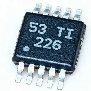
ACS712 - Hall-Effect Linear Current Sensor IC | Allegro MicroSystems
料号: ACS712 ✗ 停产| 数量 | 单价 | 小计 |
|---|---|---|
| 1 | $1.95 | $1.95 |
| 10 | $1.72 | $17.20 |
| 100 | $1.48 | $148.00 |
| 500 | $1.31 | $655.00 |
| 1,000 | $1.16 | $1,160.00 |
ACS712 概述
A Hall-effect current sensor is a non-contact transducer that exploits the Lorentz force principle: current flowing through an internal low-resistance copper conduction path generates a magnetic field proportional to the amperage, which an on-chip Hall element converts into a ratiometric analog output voltage. This places Hall-effect current sensors at the same level in the sensing hierarchy as shunt-resistor amplifiers (e.g., INA219) and current transformers (CTs); Hall sensors are uniquely galvanically isolated, compact, and bidirectional by construction, while shunt amplifiers offer higher bandwidth and CTs require AC excitation.
Key features include a galvanically isolated current path (no shunt resistor required), sub-ohm internal conductor resistance (1.2 mΩ typical) for minimal insertion loss, a 5.0 µs output rise time in response to step input, and a 50 kHz small-signal bandwidth. The device operates from a single 5 V supply, draws a low quiescent current, and provides a stable zero-current output of VCC/2 (≈2.5 V at 5 V supply) for bidirectional measurement around the mid-rail. Proprietary integrated digital temperature compensation trims sensitivity and offset across the −40°C to +85°C operating range.
The architecture uses a precise, low-offset linear Hall circuit placed near the copper conduction path; close proximity between magnetic signal and transducer maximizes device accuracy. Differential sensing cancels external stray fields, and a low-impedance output stage buffers the ratiometric output for direct connection to an ADC input or comparator threshold.
Typical applications include motor control and load detection in robotics and white goods, switched-mode power supply feedback for overcurrent protection, battery management in e-bikes and UPS systems, and 3D printer / CNC spindle current monitoring. The SOIC-8 footprint suits both hand-soldered breakouts and high-density SMT production. When designing, place a low-ESR bypass capacitor close to VCC and route the primary current conductor through the on-package copper trace to maintain specified accuracy; verify the output zero point at no current before each conversion to remove thermal drift.
直接替换替代料: ACS712 ——相同封装,引脚兼容。需要 PCB 改动的不同封装料号已排除。
快速对比工具——选择替代料号进行并排对比:
ACS724LLCTR-05B
✅ 直接替换📋 参考替代料(不在目录中)
ACS724LLCTR-20A
✅ 直接替换📋 参考替代料(不在目录中)
ACS724LLCTR-30A
✅ 直接替换📋 参考替代料(不在目录中)
ACS723LLCTR-05AB
✅ 直接替换📋 参考替代料(不在目录中)
ACS723LLCTR-20AB
✅ 直接替换📋 参考替代料(不在目录中)
ACS758LCB-050B-PFF-T
✅ 直接替换📋 参考替代料(不在目录中)
ACS712 最大额定值与电气特性
| 传感器类型 | Hall-Effect, Linear, Open-Loop |
| Number of Channels | 1 |
| Primary-Side Current Range (±5A variant) | ±5 A (ACS712ELCTR-05B-T) |
| Primary-Side Current Range (±20A variant) | ±20 A (ACS712ELCTR-20A-T) |
| Primary-Side Current Range (±30A variant) | ±30 A (ACS712ELCTR-30A-T) |
| Sensitivity (±5A variant) | 185 mV/A (typical) |
| Sensitivity (±20A variant) | 100 mV/A (typical) |
| Sensitivity (±30A variant) | 66 mV/A (typical) |
| Zero-Current Output Voltage | VCC/2 (≈2.5 V at 5 V supply) |
| Supply Voltage (VCC) | 4.5 V to 5.5 V (5 V typical) |
| Internal Conductor Resistance | 1.2 mΩ (typical) |
| Output Response Time | 5 µs (typical, di/dt = Ip/A) |
| Small-Signal Bandwidth | 50 kHz |
| 工作温度范围 | -40°C to +85°C |
| Current Direction | Bidirectional (AC and DC) |
| 封装 | 8-SOIC (3.90 mm width), surface mount |
ACS712 引脚配置
| 引脚 1 | VCC — 5 V power supply input |
| 引脚 2 | OUT — Ratiometric analog voltage output (VCC/2 at zero current) |
| 引脚 3 | FILTER — External bandwidth-setting capacitor; leave open for full bandwidth or connect 1 nF to GND to limit bandwidth |
| 引脚 4 | GND — Common ground |
| 引脚 5 | IP+ — Primary current input/conduction pin (high-current path) |
| 引脚 6 | IP+ — Primary current input/conduction pin (paralleled internally with pin 5) |
| 引脚 7 | IP- — Primary current return/conduction pin (high-current path) |
| 引脚 8 | IP- — Primary current return/conduction pin (paralleled internally with pin 7) |
典型应用
ACS712 适用于 6 应用s: BLDC Motor Control and Inverter Feedback, Switched-Mode Power Supply Overcurrent Protection, Battery Management and E-Bike Current Monitoring, Robotics and 3D Printer Load Detection, Industrial PLC and Load Monitoring, Mains AC Current Monitoring and Smart Meters.
BLDC Motor Control and Inverter Feedback
The ACS712 is used as a non-isolated analog feedback element in low-voltage brushless DC motor control loops, providing a ratiometric proportional output that scales linearly with phase current. With 50 kHz small-signal bandwidth and 5 µs step response, the device can resolve PWM-edge current ripple for sensorless FOC firmware; the VCC/2 zero-current reference is convenient for ADC sampling around mid-rail. Compared with shunt-resistor amplifiers, the ACS712's galvanically isolated copper conductor introduces no common-mode swing to the low-voltage control electronics, simplifying PCB layout.
推荐
Switched-Mode Power Supply Overcurrent Protection
In AC/DC and DC/DC converters, the ACS712 measures primary-side or secondary-side current with galvanic isolation, enabling safe overcurrent thresholding and hiccup-mode fault response in Switched-Mode Power Supply (SMPS) designs. The 50 kHz bandwidth comfortably spans the typical 50/60 Hz mains and 1-2 kHz switching frequencies used in power-factor-correction circuits, while the 1.2 mΩ internal conductor resistance minimises insertion loss. Its ratiometric output can be compared directly with a comparator reference to trigger a controller's fault pin.
推荐
Battery Management and E-Bike Current Monitoring
The ACS712 measures pack charge and discharge current on electric bicycles, scooters, and uninterruptible power supplies without breaking the high-current loop with a shunt and amplifier. The ±30 B variant monitors up to ±30 A continuously with 66 mV/A sensitivity, providing accurate SoC feedback to the battery management microcontroller. Integrated temperature compensation keeps the reading stable from cold-start (−40°C) to mid-pack discharge, while the bidirectional ratiometric output is sampled directly at the BMS AFE.
推荐
Robotics and 3D Printer Load Detection
In robotic arm and 3D printer motor control, the ACS712 senses per-driver load current to detect end-effector collisions, stalled steppers, and extruder jams. The 185 mV/A sensitivity of the −05B variant gives high-resolution measurement of small motor currents, while the 5 µs response time triggers a stall interrupt inside one PWM cycle of the fault being detected. Galvanic isolation simplifies high-current motor routing and keeps 5 V logic out of the high-current loop, an important factor in low-cost 3D printers.
推荐
Industrial PLC and Load Monitoring
The ACS712 is widely deployed on industrial Programmable Logic Controller (PLC) analogue input modules and load-management relays to measure current on each phase of a motor or heater without external shunts. The wide operating temperature range (−40°C to +85°C) and factory-trimmed sensitivity across variants support multi-load control panels spanning −05B, −20A, and −30B for mixed current ratings. The SOIC-8 surface-mount package suits both wave-soldered backplanes and reflow-printed daughter cards in industrial environments.
推荐
Mains AC Current Monitoring and Smart Meters
For line-voltage AC current sensing in smart meters, energy-monitoring outlets, and home energy displays, the ACS712 measures 50/60 Hz mains current with full galvanic isolation from low-voltage electronics. The 50 kHz bandwidth captures up to several harmonics for power-quality analysis, and the bidirectional centre-tap output directly represents the AC waveform without rectification. Using the ACS712, designers avoid the bulky current transformer footprint or the safety hazard of a direct shunt in line-voltage conductors.
推荐
推荐产品汇总
工程参考数据: ACS712 ——对比、设计指导和合规信息。
选型指南
与替代料对比
| 参数 | 本产品 | ACS724LLCTR-05B | ACS724LLCTR-20A | ACS724LLCTR-30A | ACS723LLCTR-05AB | ACS758LCB-050B-PFF-T |
|---|---|---|---|---|---|---|
| Brand | Allegro MicroSystems | Allegro MicroSystems | Allegro MicroSystems | Allegro MicroSystems | Allegro MicroSystems | Allegro MicroSystems |
| Package | 8-SOIC (LC) | 8-SOIC - same | 8-SOIC - same | 8-SOIC - same | 8-SOIC - same | 8-SOIC - same |
| Primary-Side Current Range (matched variant) | ±5 A / ±20 A / ±30 A | ±5 A | ±20 A | ±30 A | ±5 A | ±50 A |
| Sensitivity (matched variant) | 185 / 100 / 66 mV/A | 80 mV/A (lower than 185 mV/A on -05B) | 40 mV/A (lower than 100 mV/A on -20A) | 26 mV/A (lower than 66 mV/A on -30A) | 264 mV/A (higher than 185 mV/A on -05B) | 40 mV/A (lower than 66 mV/A on -30B) |
| Small-Signal Bandwidth | 50 kHz | 120 kHz (2.4x) | 120 kHz (2.4x) | 120 kHz (2.4x) | 40 kHz (slightly lower) | 120 kHz (2.4x) |
| Internal Conductor Resistance | 1.2 mΩ | 1.2 mΩ (same) | 1.2 mΩ (same) | 1.2 mΩ (same) | 0.6 mΩ (50% lower) | 0.1 mΩ (~12x lower) |
| Supply Voltage | 5.0 V (single) | 3.3 V or 5 V (dual variant) | 3.3 V or 5 V (dual variant) | 3.3 V or 5 V (dual variant) | 3.3 V or 5 V (dual variant) | 3.3 V or 5 V (dual variant) |
| Lifecycle Status | NRND (recommended new designs use ACS724/ACS723) | Active (recommended) | Active (recommended) | Active (recommended) | Active | Active |
关键差异点
- Galvanic isolation with Hall-effect measurement (对比 INA219 (shunt + amplifier))
- Direct ratiometric analog output (对比 INA219 (I2C digital))
- Three factory-trimmed current ranges in one family (对比 DRV425 shunt sensor)
- Higher bandwidth than typical isolation amplifiers (对比 AMC1301 isolation amplifier + shunt)
设计说明
Estimated: Solid two-layer / four-layer PCB thermal management. The ACS712 dissipates power in proportion to primary current squared (P = I² × 1.2 mΩ typical conductor resistance). At ±20 A continuous operation the on-chip loss is roughly 0.48 W; at ±30 A peak load (overload) it approaches 1.08 W. Use 2 oz copper pour on the IP+/IP− traces, copper via arrays under the exposed SOIC thermal land, and minimum 50 mil primary-side trace width on each terminal to keep primary-current trace heating below 10°C rise.
Estimated: ADC sampling and zero-current calibration. The ACS712 has a quiescent zero-current offset that drifts ±20 mV over the −40°C to +85°C range and per-device variations of ±30 mV. Software should average several ADC samples and subtract an at-rest offset, OR use a low-side ADC reference tied to VCC so the VCC/2 ratiometric drift is automatically cancelled. Failing to recalibrate offset after long thermal settling produces apparent ghost currents of ~50-150 mA. Also, never leave FILTER pin floating in noisy environments; tying 1 nF to GND reduces high-frequency noise reaching the output.
Route primary current through all four IP+ / IP− pins and use proper magnetic isolation. The four conduction pins (1-4 group and 5-8 group) must be soldered to a wide PCB trace or pad capable of carrying the full primary current; missing any one will create current crowding and thermal stress. Maintain ≥6 mm clearance between the IP+/IP− high-current traces and OUT/FILTER low-level traces; never place a ground plane directly under the IP+ conductor to avoid creating an unintended low-resistance shunt path. Place the 100 nF VCC bypass and any FILTER capacitor within 5 mm of their respective pins for stable measurement.
合规信息
RoHS and REACH compliant per Allegro product literature; ACS712 is NOT AEC-Q100 qualified - design automotive-grade systems using the ACS724-Q1 or ACS758-Q1 variants with explicit Q1 part numbers.