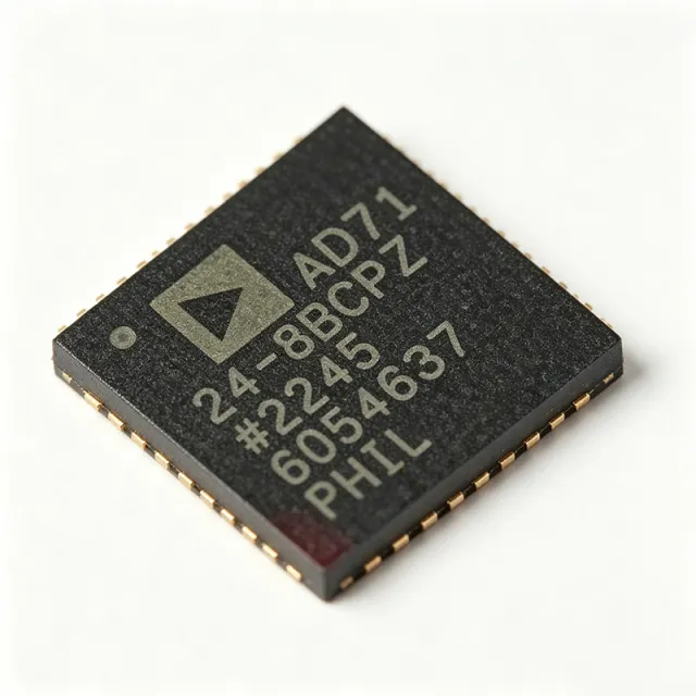
AD7124-8BCPZ - 24-Bit Sigma-Delta AFE, 8-Ch, PGA | Analog Devices
料号: AD7124-8BCPZ ✓ 量产中| 数量 | 单价 | 小计 |
|---|---|---|
| 1 | $11.5 | $11.50 |
| 10 | $10.35 | $103.50 |
| 100 | $8.95 | $895.00 |
| 500 | $8.2 | $4,100.00 |
| 1,000 | $7.45 | $7,450.00 |
| 2,500 | $6.95 | $17,375.00 |
AD7124-8BCPZ 概述
An analog-to-digital converter is a mixed-signal device that converts continuous analog signals into discrete digital codes, and a sigma-delta ADC is one of the most accurate architectures, using oversampling and noise-shaping to push quantization noise out of the signal band. Within the data converter hierarchy, the AD7124-8 is not just an ADC - it is a complete analog front end (AFE) that combines the modulator, digital filter, PGA, and reference into a single die, placing it above simple SAR or stand-alone sigma-delta converters in system integration. By eliminating the external precision reference and most of the input signal conditioning, the AD7124-8 collapses the typical sensor-measurement signal chain into a single device. Key features include 24-bit resolution, RMS noise as low as 1.8 uV at the 25 SPS output data rate, typical full-power-mode current of 1.2 mA, a programmable output data rate from 1.17 SPS to 19.2 kSPS, and an integrated PGA with gains from 1 to 128 for direct connection to low-level sensors such as thermocouples and strain gauges. Three user-programmable power modes (full, mid, low) allow designers to trade off noise against supply current at the system level. Architecturally, the second-order sigma-delta modulator feeds a configurable digital filter, and the device offers simultaneous-50Hz/60Hz-rejection modes for industrial instrumentation. The 24-bit register map and SPI-compatible serial interface simplify integration with microcontrollers and DSPs. Typical applications include direct thermocouple and RTD temperature measurement, weigh scales, pressure and flow transmitters, industrial process-control analog input modules, and battery-cell monitoring. A design tip: bypass AVDD and DVDD with separate 10 uF and 0.1 uF capacitors, use a clean analog ground plane, and populate REFIN+/FOUT inputs with a 10 uF capacitor to keep reference noise below the ADC noise floor. Prices are referenced as of 2026-10-06 from distributor stock.
直接替换替代料: AD7124-8BCPZ ——相同封装,引脚兼容。需要 PCB 改动的不同封装料号已排除。
本系列中的变体
可与以下型号直接替换的同系列型号: AD7124-8BCPZ (相同外形与封装尺寸) ——差异在于 Operating Temperature Range, Package, Analog Supply Voltage, Digital Supply Voltage, Interface.
快速对比工具——选择替代料号进行并排对比:
AD7124-8BCPZ-RL7
✅ 直接替换✓ 有现货
$8.85 / 个
查看数据手册 →AD7124-8WBCPZ
✅ 直接替换📋 参考替代料(不在目录中)
AD7124-8WBCPZ-RL7
✅ 直接替换📋 参考替代料(不在目录中)
AD7175-8BCPZ
✅ 直接替换✓ 有现货
$20.82 / 个
查看数据手册 →AD7175-8BCPZ-RL7
✅ 直接替换✓ 有现货
$8.32 / 个
查看数据手册 →AD7124-8BCPZ 最大额定值与电气特性
| 分辨率 | 24 bits |
| ADC Architecture | Sigma-Delta |
| Number of Input Channels | 8 differential / 15 pseudo-differential |
| Maximum Output Data Rate | 19.2 kSPS |
| Minimum Output Data Rate | 1.17 SPS |
| Analog Supply Voltage (AVDD) | 2.7 V to 3.6 V |
| Digital Supply Voltage (DVDD) | 1.65 V to 3.6 V |
| RMS Noise (lowest, gain = 1) | 1.8 uV at 25 SPS (typical) |
| Integrated PGA Gain Range | 1 to 128 |
| Integrated Reference | Internal 2.5 V low-drift bandgap (with external REF input option) |
| Supply Current (full power mode) | 1.2 mA typical |
| 接口 | SPI (4-wire, serial) |
| 工作温度范围 | -40C to +125C |
| 封装 | 32-lead LFCSP (5x5 mm) |
| 安装类型 | Surface Mount |
| AEC-Q100 Qualification | W grade variant is AEC-Q100 qualified (AD7124-8WBCPZ) |
| RoHS 状态 | Compliant |
| REACH Status | Compliant (REACH Unaffected per third-party data) |
AD7124-8BCPZ 引脚配置
| 引脚 1 | AVDD — Analog supply voltage (2.7V to 3.6V) |
| 引脚 2 | AVSS — Analog ground |
| 引脚 3 | REFIN1+ — Positive reference input 1 |
| 引脚 4 | REFIN1- — Negative reference input 1 |
| 引脚 5 | AIN0 — Analog input 0 |
| 引脚 6 | AIN1 — Analog input 1 |
| 引脚 7 | AIN2 — Analog input 2 |
| 引脚 8 | AIN3 — Analog input 3 |
| 引脚 9 | AIN4 — Analog input 4 |
| 引脚 10 | AIN5 — Analog input 5 |
| 引脚 11 | AIN6 — Analog input 6 |
| 引脚 12 | AIN7 — Analog input 7 |
| 引脚 13 | AIN8 — Analog input 8 (pseudo-differential only) |
| 引脚 14 | AIN9 — Analog input 9 (pseudo-differential only) |
| 引脚 15 | AIN10 — Analog input 10 (pseudo-differential only) |
| 引脚 16 | AIN11 — Analog input 11 (pseudo-differential only) |
| 引脚 17 | AIN12 — Analog input 12 (pseudo-differential only) |
| 引脚 18 | AIN13 — Analog input 13 (pseudo-differential only) |
| 引脚 19 | AIN14 — Analog input 14 (pseudo-differential only) |
| 引脚 20 | REFIN2+ — Positive reference input 2 |
| 引脚 21 | REFIN2- — Negative reference input 2 |
| 引脚 22 | IOVDD — Digital I/O supply voltage |
| 引脚 23 | DOUT/RDY — SPI data output / ready signal |
| 引脚 24 | DIN — SPI data input |
| 引脚 25 | SCLK — SPI serial clock |
| 引脚 26 | SYNC/CSLAVE — SPI chip select / synchronization input |
| 引脚 27 | RESET — Reset input (active low) |
| 引脚 28 | DVDD2 — Digital supply voltage 2 |
| 引脚 29 | DGND — Digital ground |
| 引脚 30 | GPIO0 — General-purpose I/O 0 / crystal oscillator input |
| 引脚 31 | GPIO1 — General-purpose I/O 1 / crystal oscillator output |
| 引脚 32 | AVSS — Analog ground (secondary) |
典型应用
AD7124-8BCPZ 适用于 6 应用s: Thermocouple Temperature Measurement, RTD and Thermistor Conditioning, Weigh Scale / Load Cell Digitization, Industrial Process Control Analog Input Modules, Battery Cell Monitoring (BMS), Pressure and Flow Transmitters.
Thermocouple Temperature Measurement
The AD7124-8BCPZ is ideally suited for thermocouple temperature measurement because its integrated PGA provides gain up to 128 and its 1.8 uV RMS noise floor at 25 SPS is below the thermoelectric voltage of a K-type thermocouple at sub-degree resolution. Placed directly across a type-K, J, or T thermocouple, the device amplifies the millivolt-level signal to a usable range while digitizing at 24-bit resolution, eliminating a dedicated instrumentation amplifier. Designers should configure the device in low-power mode with a 25 SPS or 50 SPS output data rate for simultaneous 50 Hz / 60 Hz mains rejection. According to the Analog Devices datasheet, the integrated cold-junction compensation is supported by tying one channel to a separate silicon diode sensor.
推荐
RTD and Thermistor Conditioning
The AD7124-8BCPZ digitizes both 2-wire, 3-wire, and 4-wire RTDs as well as NTC thermistors by using its pseudo-differential input channels to excite and read the resistive sensor. Its low-drift internal 2.5 V bandgap reference provides the excitation current with better than 10 ppm/C stability, and the integrated PGA enables direct connection to PT100 / PT1000 RTDs without an external instrumentation amplifier. The on-chip matched current sources for RTD excitation reduce calibration complexity, and the digital filter supports 50 Hz and 60 Hz synchronous rejection. Per the AD7124-8 datasheet, the device is suitable for industrial-grade temperature controllers with accuracy better than 0.1 C over the -40C to +125C operating range.
推荐
Weigh Scale / Load Cell Digitization
The AD7124-8BCPZ is well matched to load-cell and strain-gauge weigh scales because the integrated PGA gain of 128 amplifies the few-mV full-scale bridge output to span most of the ADC input range. A 1 kg / 5 kg / 50 kg load cell excited at 5 V produces a few mV full-scale output, well within the AD7124-8BCPZ input range when PGA = 128 is selected. With its 21 noise-free bits at 25 SPS, the device delivers better than 1 part in 100,000 resolution, satisfying OIML and NTEP weigh-scale accuracy requirements. According to the Analog Devices datasheet, the device is suitable for direct bridge excitation of 350 ohm and 1 kohm load cells without an external instrumentation amplifier.
推荐
Industrial Process Control Analog Input Modules
The AD7124-8BCPZ integrates 8 differential inputs in a single 32-LFCSP (5x5 mm) package, which is ideal for multi-channel analog input modules on PLC backplanes and process-control transmitters. The 4-wire SPI interface connects to typical microcontrollers and DSPs used in industrial PLCs, while the integrated PGA simplifies 4-20 mA current-loop voltage digitization. The device operates from -40C to +125C and is suitable for IEC 61000-4 industrial EMC environments. According to the Analog Devices datasheet, the simultaneous 50 Hz / 60 Hz rejection at 25 SPS output data rate improves effective resolution in factory environments.
推荐
Battery Cell Monitoring (BMS)
The AD7124-8BCPZ is suitable for multi-cell battery monitoring in lithium-ion battery packs and UPS systems because the 8 differential input channels digitize individual cell voltages with 24-bit resolution and 1.8 uV noise floor. Placed across each cell of a 4S to 8S lithium pack, the device synchronously samples the cell voltage stack while the integrated PGA handles the 4.2 V max cell voltage at gain = 1. The low-power mode draws under 350 uA per channel, suitable for always-on BMS ICs. According to the AD7124-8 datasheet, the SPI interface enables connection to typical BMS controllers for cell balancing decisions.
推荐
Pressure and Flow Transmitters
The AD7124-8BCPZ is well matched to pressure transmitters and flow meters because the integrated PGA gain of 128 amplifies the millivolt-level bridge output of typical pressure sensors and Coriolis flow tubes. With 21 noise-free bits at 25 SPS, the device delivers the 0.05% accuracy needed by HART-protocol pressure transmitters. The on-chip current sources for sensor excitation and the integrated low-drift reference simplify loop-powered 4-20 mA transmitter designs, while the SPI interface connects to typical low-power MCUs. According to the Analog Devices datasheet, the device operates from -40C to +125C suitable for outdoor field-mount pressure transmitters.
推荐
推荐产品汇总
工程参考数据: AD7124-8BCPZ ——对比、设计指导和合规信息。
选型指南
与替代料对比
| 参数 | 本产品 | AD7124-8BCPZ-RL7 | AD7124-8WBCPZ | AD7124-8WBCPZ-RL7 | AD7175-8BCPZ | AD7175-8BCPZ-RL7 |
|---|---|---|---|---|---|---|
| Brand | Analog Devices | Analog Devices | Analog Devices | Analog Devices | Analog Devices | Analog Devices |
| Package | 32-LFCSP (5x5 mm) | 32-LFCSP (5x5 mm) - same | 32-LFCSP (5x5 mm) - same | 32-LFCSP (5x5 mm) - same | 32-LFCSP (5x5 mm) - same | 32-LFCSP (5x5 mm) - same |
| Resolution | 24-bit | 24-bit | 24-bit | 24-bit | 24-bit | 24-bit |
| Input Channels | 8 diff / 15 pseudo-diff | 8 diff / 15 pseudo-diff | 8 diff / 15 pseudo-diff | 8 diff / 15 pseudo-diff | 8 diff / 16 single-ended | 8 diff / 16 single-ended |
| Maximum Output Data Rate | 19.2 kSPS | 19.2 kSPS | 19.2 kSPS | 19.2 kSPS | 625 kSPS | 625 kSPS |
| Integrated PGA | Yes (gain 1 to 128) | Yes (gain 1 to 128) | Yes (gain 1 to 128) | Yes (gain 1 to 128) | No | No |
| RMS Noise @ lowest rate | 1.8 uV @ 25 SPS | 1.8 uV @ 25 SPS | 1.8 uV @ 25 SPS | 1.8 uV @ 25 SPS | 8.5 uV @ 10 kSPS | 8.5 uV @ 10 kSPS |
| AEC-Q100 Qualified | No (W grade available) | No (W grade available) | Yes | Yes | No | No |
关键差异点
- Highest signal-chain integration in 32-LFCSP (5x5 mm) (对比 AD7124-4BRUZ)
- Integrated PGA (gain up to 128) eliminates external in-amp (对比 AD7175-8BCPZ)
- AEC-Q100 W grade available in same footprint (对比 AD7124-8BCPZ (B grade standard))
- Versus -RL7 (packaging variant) (对比 AD7124-8BCPZ-RL7)
设计说明
Power the AD7124-8BCPZ from a low-noise LDO such as the ADM7150 or ADP150 placed close to the AVDD pin, with separate 10 uF and 0.1 uF ceramic capacitors on each AVDD and DVDD pin pair. The analog and digital grounds must meet at one star-point, ideally beneath the LFCSP exposed pad (EP), which must be soldered to a low-impedance analog ground plane to dissipate thermal dissipation and to provide the lowest-impedance return for the integrated reference.
Route analog input traces as differential pairs with constant 50 ohm or 100 ohm impedance, keeping traces short and matched in length to avoid mismatch errors that degrade common-mode rejection. Place input RC anti-alias filters (typically 1 kohm + 1 nF) within 5 mm of each analog input pin. The REFIN1+/REFIN1- traces should be guarded with analog ground and bypassed with a 10 uF capacitor to keep reference noise below the ADC noise floor.
Do not exceed AVDD = 3.6 V; absolute maximum on AVDD is 5 V only when the overvoltage protection clamps engage, and sustained overvoltage damages the input ESD structures. Do not enable more than 8 differential channels - the pseudo-differential AIN8..AIN14 channels cannot be used as a true differential pair. Configure the SPI SCLK at or below 10 MHz in low-power mode and at or below 20 MHz in full-power mode; faster clocks corrupt the digital filter settling.
Use the simultaneous 50 Hz / 60 Hz rejection mode at 25 SPS output data rate for industrial applications to suppress mains-induced noise on analog inputs. For thermocouple measurements, configure the device with PGA gain = 128 to amplify the millivolt-level thermoelectric voltage to span the ADC input range, and use a separate silicon diode channel for cold-junction compensation. The digital filter settling time requires a full conversion cycle after any input channel or gain change.
合规信息
Standard B grade is not AEC-Q100; AEC-Q100 grade is the AD7124-8WBCPZ. RoHS compliant per Analog Devices product page. REACH unaffected per third-party data (PartGenie).







