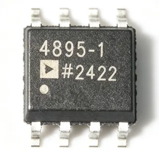
ADA4522-2ARZ-RL7 - Dual 55V Zero-Drift Op Amp | Analog Devices
料号: ADA4522-2ARZ-RL7 ✓ 量产中| 数量 | 单价 | 小计 |
|---|---|---|
| 1 | $3.42 | $3.42 |
| 10 | $3.08 | $30.80 |
| 100 | $2.74 | $274.00 |
| 500 | $2.47 | $1,235.00 |
| 1,000 | $2.19 | $2,190.00 |
ADA4522-2ARZ-RL7 概述
Zero-drift amplifiers, also known as chopper-stabilized or auto-zero amplifiers, are a class of operational amplifiers that continuously correct their input offset voltage and drift, achieving near-zero offset and extremely low offset drift over temperature and time. This makes them ideal for precision signal conditioning, sensor interfaces, and instrumentation where accuracy is paramount. The ADA4522-2 belongs to the family of zero-drift op amps, which are a subset of precision operational amplifiers, which in turn fall under the broader category of linear integrated circuits.
Key features of the ADA4522-2 include a maximum offset voltage of 5 µV, an extremely low offset voltage drift of 22 nV/°C, and a low voltage noise density of 5.8 nV/√Hz typical. The input bias current is only 50 pA typical, and the device provides 117 nV p-p typical noise from 0.1 Hz to 10 Hz. The amplifier also features on-chip EMI filtering, achieving high immunity to electromagnetic interference, and is fully specified over the extended industrial temperature range.
The ADA4522-2 uses a proprietary zero-drift architecture that combines a precision CMOS input stage with a chopper stabilization technique. This results in excellent DC accuracy and low noise, making it suitable for high-resolution data acquisition systems, precision current sensing, and bridge amplifiers. The rail-to-rail output stage allows maximum dynamic range, and the ground-sensing inputs enable true single-supply operation.
Typical applications include precision instrumentation, medical devices, industrial process control, and automotive sensor interfaces. The wide supply voltage range and low noise make it particularly well-suited for battery-powered and high-voltage systems. The device is also available in single (ADA4522-1) and quad (ADA4522-4) versions, providing design flexibility.
When designing with the ADA4522-2, it is important to provide proper decoupling on the power supply pins and to consider the effects of input bias current on high-impedance sources. The device's low offset and drift eliminate the need for external trimming in most applications, simplifying the design and improving long-term reliability.
直接替换替代料: ADA4522-2ARZ-RL7 ——相同封装,引脚兼容。需要 PCB 改动的不同封装料号已排除。
本系列中的变体
可与以下型号直接替换的同系列型号: ADA4522-2ARZ-RL7 (相同外形与封装尺寸) ——差异在于 Package, Amplifier Type, Operating Temperature Range, RoHS Status, Supply Voltage Range.
快速对比工具——选择替代料号进行并排对比:
ADA4522-2ARZ
✅ 直接替换✓ 有现货
$3.9 / 个
查看数据手册 →ADA4522-2ARZ-R7
✅ 直接替换📋 参考替代料(不在目录中)
ADA4522-1ARZ
✅ 直接替换✓ 有现货
$1.42 / 个
查看数据手册 →OPA2189
✅ 直接替换 ⚠️ 规格未核验📋 参考替代料(不在目录中)
LTC2057
✅ 直接替换 ⚠️ 规格未核验📋 参考替代料(不在目录中)
ADA4522-2ARZ-RL7 最大额定值与电气特性
| Number of Channels | 2 |
| Supply Voltage Range | 4.5 V to 55 V |
| Supply Voltage Range (Dual) | ±2.25 V to ±27.5 V |
| Offset Voltage (Max) | 5 µV |
| Offset Voltage Drift (Max) | 22 nV/°C |
| Voltage Noise Density (Typ) | 5.8 nV/√Hz |
| Input Bias Current (Typ) | 50 pA |
| Noise (0.1 Hz to 10 Hz) | 117 nV p-p typical |
| 输出类型 | Rail-to-Rail |
| Input Type | Ground-Sensing |
| EMI Immunity | Enhanced (on-chip filtering) |
| 工作温度范围 | -40°C to +125°C |
| 封装 | 8-Lead SOIC (SOIC-8) |
| 安装类型 | Surface Mount |
| Amplifier Type | Zero-Drift |
ADA4522-2ARZ-RL7 引脚配置
| 引脚 1 | OUT A — Output of amplifier A |
| 引脚 2 | -IN A — Inverting input of amplifier A |
| 引脚 3 | +IN A — Non-inverting input of amplifier A |
| 引脚 4 | V- — Negative supply (or ground in single-supply operation) |
| 引脚 5 | +IN B — Non-inverting input of amplifier B |
| 引脚 6 | -IN B — Inverting input of amplifier B |
| 引脚 7 | OUT B — Output of amplifier B |
| 引脚 8 | V+ — Positive supply |
典型应用
ADA4522-2ARZ-RL7 适用于 6 应用s: Precision Instrumentation, Medical Devices, Industrial Process Control, Automotive Sensor Interfaces, Test and Measurement, Energy Harvesting Systems.
Precision Instrumentation
The ADA4522-2ARZ-RL7's ultra-low offset voltage (5 µV max) and drift (22 nV/°C) make it ideal for precision instrumentation such as data acquisition systems, weigh scales, and bridge amplifiers. Its low noise (5.8 nV/√Hz) ensures accurate measurement of small signals, while the wide supply range (up to 55V) accommodates industrial sensor interfaces. The ground-sensing inputs allow true single-supply operation, simplifying design in battery-powered instruments.
推荐
Medical Devices
In medical devices such as patient monitors and diagnostic equipment, the ADA4522-2ARZ-RL7 provides the accuracy and low noise required for biosignal amplification. Its low input bias current (50 pA) minimizes errors when interfacing with high-impedance electrodes, and the rail-to-rail output maximizes dynamic range for ADC interfaces. The extended temperature range (-40°C to +125°C) ensures reliable operation in clinical environments.
推荐
Industrial Process Control
The ADA4522-2ARZ-RL7 is well-suited for industrial process control loops, where long-term stability and accuracy are critical. Its zero-drift architecture eliminates offset drift over temperature, reducing calibration requirements. The wide supply voltage (up to 55V) allows direct interfacing with 24V industrial buses, and the enhanced EMI immunity ensures reliable operation in noisy factory environments. The device can be used in PID controllers, valve positioners, and pressure transmitters.
推荐
Automotive Sensor Interfaces
For automotive sensor interfaces, the ADA4522-2ARZ-RL7 offers the precision and robustness needed for applications like battery monitoring, motor control, and pressure sensing. Its wide supply range (up to 55V) handles automotive battery voltage transients, and the low offset drift ensures accurate measurement over the -40°C to +125°C temperature range. The ground-sensing inputs enable high-side and low-side current sensing without level shifting.
推荐
Test and Measurement
In test and measurement equipment, the ADA4522-2ARZ-RL7 provides the accuracy and low noise required for high-resolution measurements. Its low offset and drift enable precise DC measurements, while the wide bandwidth and rail-to-rail output support AC signal conditioning. The device is ideal for use in digital multimeters, source measure units, and precision voltage references. The enhanced EMI immunity ensures accurate readings in electrically noisy environments.
推荐
Energy Harvesting Systems
The ADA4522-2ARZ-RL7 is suitable for energy harvesting systems where low power consumption and high accuracy are essential. Its low quiescent current and wide supply range allow operation from variable energy sources such as solar cells and thermoelectric generators. The zero-drift architecture ensures accurate signal conditioning of small sensor outputs, and the rail-to-rail output maximizes the usable signal range for energy-efficient ADCs.
推荐
推荐产品汇总
工程参考数据: ADA4522-2ARZ-RL7 ——对比、设计指导和合规信息。
选型指南
与替代料对比
| 参数 | 本产品 | ADA4522-2ARZ | ADA4522-2ARZ-R7 | OPA2189 | LTC2057 |
|---|---|---|---|---|---|
| Package | 8-SOIC | 8-SOIC | 8-SOIC | 8-SOIC | 8-SOIC |
| Brand | Analog Devices | Analog Devices | Analog Devices | Texas Instruments | Analog Devices |
| Number of Channels | 2 | 2 | 2 | 2 | 2 |
| Supply Voltage Range | 4.5V to 55V | 4.5V to 55V | 4.5V to 55V | 4.5V to 36V | 4.75V to 36V |
| Offset Voltage (Max) | 5 µV | 5 µV | 5 µV | 4 µV | 0.5 µV |
| Offset Drift (Max) | 22 nV/°C | 22 nV/°C | 22 nV/°C | 0.04 µV/°C | 0.01 µV/°C |
| Voltage Noise Density | 5.8 nV/√Hz | 5.8 nV/√Hz | 5.8 nV/√Hz | 5.2 nV/√Hz | 7.5 nV/√Hz |
| Input Bias Current | 50 pA | 50 pA | 50 pA | 150 pA | 20 pA |
关键差异点
- Wide supply voltage range up to 55V (对比 OPA2189)
- Enhanced EMI immunity (对比 LTC2057)
- Ground-sensing inputs (对比 OPA2189)
设计说明
The ADA4522-2ARZ-RL7 operates from 4.5V to 55V. For best performance, use a low-noise power supply and place a 0.1µF ceramic capacitor close to each supply pin (V+ and V-). For single-supply operation, connect V- to ground and ensure the input common-mode range includes ground (ground-sensing inputs).
To minimize noise pickup, keep the input traces short and shielded. Use a solid ground plane under the device and avoid routing high-frequency digital signals near the inputs. The ADA4522-2 has enhanced EMI immunity, but proper layout still improves performance. Place decoupling capacitors as close as possible to the supply pins.
Do not exceed the absolute maximum supply voltage of 60V. Also, ensure the input voltages do not exceed the supply rails. The device has internal ESD protection, but external protection diodes may be needed for harsh environments. For high-impedance sources, consider the input bias current (50 pA) and use a guard ring if necessary.
合规信息
RoHS compliant per Analog Devices product page. Not AEC-Q100 qualified. Lead-free finish.