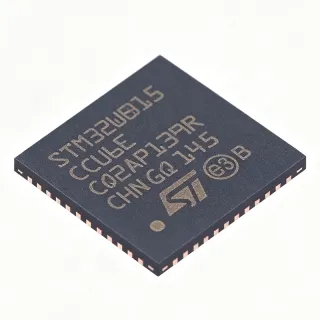
ADF4360-3BCPRL - 1.75GHz Integer-N VCO | Analog Devices
料号: ADF4360-3BCPRL ✓ 量产中ADF4360-3BCPRL 概述
An integer-N synthesizer is a clock and RF signal-generation component that generates an output frequency through feedback locking to a reference frequency. The ADF4360-3 family is intended for wireless communication, test equipment, instrumentation, and other systems requiring a programmable RF carrier with controlled phase and frequency. The divide-by-2 feature provides flexibility for systems operating below the main VCO frequency while retaining a shared synthesizer architecture.
The principal design features include the 1750 MHz VCO center-frequency designation, an RF output range of 800 MHz to 975 MHz in divide-by-2 mode, integrated integer-N operation, and a 3 V to 3.6 V supply range. The device is intended for surface-mount assembly and is identified in product listings as a 24-terminal WFQFN package with an exposed pad. Its integrated VCO reduces the number of external high-frequency components required for a complete local oscillator implementation.
In practice, the ADF4360-3BCPRL is used where a compact programmable RF source is more useful than a fixed crystal oscillator. The on-chip VCO, feedback divider, and phase-locked-loop functions make the device appropriate for RF signal generation, frequency hopping, modulation, communications test equipment, and industrial RF systems. The exact tuning range, reference-frequency limits, output-power characteristics, noise performance, and register map should be confirmed against the manufacturer datasheet before final circuit design.
The exposed-pad package requires careful PCB layout to remove heat from the die and maintain reliable electrical performance at the intended operating temperature. Place power and ground connections according to the recommended land pattern, connect the exposed pad to the appropriate ground plane, and keep sensitive reference and control traces away from noisy RF output paths. The 3 V to 3.6 V supply range also requires stable decoupling close to the device.
This product page combines the manufacturer product information, package identification, application guidance, and practical design considerations. It is intended to help engineers determine whether the ADF4360-3BCPRL matches a required RF frequency range, package footprint, supply requirement, and integration level before requesting a quotation or beginning a hardware design.
直接替换替代料: ADF4360-3BCPRL ——相同封装,引脚兼容。需要 PCB 改动的不同封装料号已排除。
本系列中的变体
可与以下型号直接替换的同系列型号: ADF4360-3BCPRL (相同外形与封装尺寸) ——差异在于 Device Type, Package, Supply Voltage Range.
ADF4360-1BCPRL
✅ 直接替换联系询价
查看数据手册 →ADF4360-4BCPZRL7
✅ 直接替换📋 参考替代料(不在目录中)
ADF4360-3BCPRL 规格参数
| Device Type | Integer-N frequency synthesizer with integrated voltage controlled oscillator |
| VCO Center Frequency | 1750 MHz |
| Divide-by-2 RF Output Range | 800 MHz to 975 MHz |
| Supply Voltage Range | 3 V to 3.6 V |
| Number of Terminals | 24 terminals |
| 封装 | 24-lead WFQFN with exposed pad |
| 安装类型 | Surface mount |
| Terminal Form | No lead |
| Package Shape | Square |
| Package Code | HVQCCN |
| Shipping Format | Tape and reel |
| Temperature Grade | Industrial |
| Frequency Synthesis Architecture | Integer-N |
| VCO Integration | Fully integrated on-chip VCO |
ADF4360-3BCPRL hvqccn 引脚配置指南
ADF4360-3BCPRL(hvqccn 封装)的引脚配置。 引脚编号、功能和连接图在制造商数据手册中定义。请参阅该手册以了解确切的封装尺寸和焊接指南。

暂无详细引脚数据: ADF4360-3BCPRL.
请参阅 数据手册 以查看完整引脚配置。
典型应用
ADF4360-3BCPRL 适用于 6 应用s: RF Communications Local Oscillator, Wireless Transmitter Carrier Generation, Frequency-Hopping Test Equipment, Industrial RF Monitoring, RF Signal-Integrity Lab, Compact RF Communication Module.
RF Communications Local Oscillator
The ADF4360-3BCPRL fits programmable RF communications systems that need an integrated source near the 1750 MHz design center. Its divide-by-2 output mode provides 800 MHz to 975 MHz, which is useful for lower-frequency carrier or local-oscillator paths. The integer-N architecture combines the VCO, feedback divider, and phase-locked-loop functions in one 24-lead WFQFN device, reducing board area and external frequency-generation components. Designers should select the reference frequency and loop settings that meet the required channel spacing, while preserving clean supply decoupling and a short RF return path.
推荐
Wireless Transmitter Carrier Generation
The ADF4360-3BCPRL is appropriate for a wireless transmitter requiring a programmable RF carrier and compact synthesizer integration. The 1750 MHz VCO center-frequency designation and the 800 MHz to 975 MHz divide-by-2 range provide useful starting points for RF front ends operating below the main VCO band. Integrating the synthesizer and VCO shortens the signal path compared with a discrete oscillator arrangement. The final design must account for output drive level, reference phase noise, loop bandwidth, and impedance matching before the carrier is connected to the transmitter chain.
推荐
Frequency-Hopping Test Equipment
The ADF4360-3BCPRL can serve as the programmable RF source in frequency-hopping and automated test equipment because it combines frequency generation with digital control in a single component. A compact WFQFN implementation is valuable where multiple test channels or compact instrumentation modules need local RF sources. The device's integer-N architecture supports programmable frequency changes through its control interface, while the integrated VCO avoids a separate high-frequency resonator network. Validate settling time, frequency accuracy, reference requirements, and permissible output power against the test specification.
推荐
Industrial RF Monitoring
The ADF4360-3BCPRL is suitable for industrial RF monitoring systems that require a stable, programmable source for sensor excitation, calibration, or signal analysis. The 3 V to 3.6 V operating range supports compact embedded equipment, and the integrated synthesizer/VCO arrangement lowers component count compared with a separated reference and VCO design. Use the divide-by-2 output when the instrumentation operates in the 800 MHz to 975 MHz region. Stable reference routing, short control traces, proper exposed-pad grounding, and controlled PCB temperature rise are essential for predictable RF performance.
推荐
RF Signal-Integrity Lab
The ADF4360-3BCPRL can provide the programmable excitation source used in an RF signal-integrity laboratory for measuring gain, filtering, modulation, or frequency response. Its integrated integer-N synthesizer makes it easier to build repeatable automated test sequences with a single compact device. The 1750 MHz design center and lower divide-by-2 range cover useful bands for communications-related measurements. For accurate results, separate sensitive measurement paths from the digital control bus, use a clean reference source, and follow the recommended exposed-pad and decoupling layout.
推荐
Compact RF Communication Module
The ADF4360-3BCPRL fits compact RF communication modules that need a local oscillator without allocating board space for discrete synthesizer components. Its 24-lead WFQFN exposed-pad package supports dense RF layouts, while the integrated integer-N and VCO functions provide a programmable output for modulation and channel-related experiments. The device operates from 3 V to 3.6 V, allowing it to fit systems with a conventional low-voltage RF rail. Care must be taken with thermal design and reference-loop layout, particularly where the synthesizer is expected to deliver high output power into a lossy antenna network.
推荐
推荐产品汇总
工程参考数据: ADF4360-3BCPRL ——对比、设计指导和合规信息。
选型指南
与替代料对比
| 参数 | 本产品 | ADF4360-1BCPRL | ADF4360-4BCPZRL7 |
|---|---|---|---|
| Package | 24-lead WFQFN with exposed pad | 24-lead WFQFN with exposed pad | 24-lead WFQFN with exposed pad |
| Brand | Analog Devices | Analog Devices | Analog Devices |
| Product Type | Integer-N synthesizer with integrated VCO | Integer-N synthesizer with integrated VCO | Integer-N synthesizer with integrated VCO |
| Number of Terminals | 24 terminals | 24 terminals | 24 terminals |
| Frequency Synthesis Architecture | Integer-N | Integer-N | Integer-N |
| Mounting Type | Surface mount | Surface mount | Surface mount |
关键差异点
- Integrated synthesizer and VCO in one compact device (对比 ADF4360-1BCPRL)
- Dedicated divide-by-2 output range (对比 ADF4360-4BCPZRL7)
- Surface-mount RF integration (对比 ADF4360-1BCPRL)
设计说明
Use the Analog Devices recommended land pattern for the 24-lead WFQFN exposed-pad package. Place the exposed-pad vias within or immediately beneath the thermal pad region, keep the ground return continuous, and place supply decoupling capacitors close to the power pins. Do not route the reference clock or digital control traces directly beneath the RF output path.
The exposed pad is the primary heat-spreading connection for this package. Provide adequate exposed-pad vias and connect the pad to the ground plane using the manufacturer's layout recommendation. Estimate junction temperature from the actual dissipation, copper area, via arrangement, and ambient temperature before operating at the upper end of the 3 V to 3.6 V supply range.
Keep the reference input and control bus short and return them through a quiet ground region. Decouple the supply locally and maintain controlled impedance for RF output routing. Because the device integrates a VCO, unstable reference or supply conditions can affect frequency stability and phase noise; validate the reference source, loop settings, and output matching in the final layout.
Do not select a frequency-band alternative solely because it uses a similar 24-lead WFQFN package. Compare the required operating band, reference-frequency limits, output power, tuning range, control-register map, and exposed-pad dimensions before treating ADF4360-1BCPRL or ADF4360-4BCPZRL7 as a replacement.
合规信息
The available product and distributor descriptions identify the device as an industrial-grade Analog Devices component but do not provide verified RoHS, REACH, lead-free, halogen-free, or conflict-minerals statements.