ICS621MIT - 1:4 200MHz Clock Buffer | Renesas Electronics
料号: ICS621MIT ✓ 量产中ICS621MIT 概述
A clock buffer is a digital timing IC that reproduces a clock signal through one or more output stages. Clock buffers and clock drivers belong to the broader clock and timing IC category, where their practical role is to isolate a source from capacitive loading, extend signal reach, and distribute a common timing reference. In a multi-load system, a buffer helps each receiver see a cleaner transition sequence than it would when connected directly to a long or heavily loaded clock trace.
The principal characteristics of ICS621MIT are its 1:4 fanout ratio, 200 MHz maximum clock frequency, low-skew architecture, and 8-SOIC package. A 1:4 ratio means that one incoming clock can feed four output branches, reducing the number of separate distribution stages required in a moderate-complexity system. The 200 MHz operating capability makes the device relevant to designs carrying clock signals in the hundreds-of-megahertz range, subject to the complete electrical limits and layout guidance in the manufacturer datasheet.
Because the ICS621MIT performs digital fanout rather than voltage conversion, its signal path is intended to preserve clock timing relationships across the four outputs. Low skew is particularly relevant when multiple receivers must operate from the same edge, including parallel data converters, sequential logic, communications equipment, and automated test systems. The exact propagation-delay, output-impedance, rise-time, fall-time, supply-voltage, and temperature limits should be taken directly from the 621 datasheet before final timing and power-budget calculations.
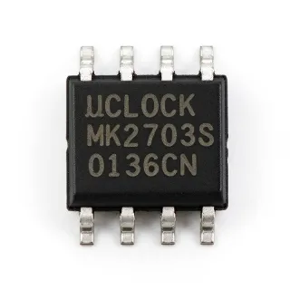
Typical uses include clock distribution for communication equipment, fanout in network interfaces, test-and-measurement systems, and synchronization among multiple digital subsystems. It can also serve as an interface between a central clock source and several low-to-moderate-capacitance loads when the board requires a dedicated fanout stage. Its eight-pin package also keeps the footprint compact while exposing one input, four outputs, power connections, and ground in a conventional small-outline arrangement.
Layout should prioritize short clock traces, a continuous ground reference, and placement of the device near the clock source or the group of receivers it serves. Avoid routing sensitive clock nets beneath unrelated noisy circuitry, and terminate or control unused outputs according to the manufacturer's guidance. Validate timing at the intended frequency, load capacitance, supply voltage, temperature, and process corner because fanout buffers can change edge rate and edge-to-edge alignment as loading changes.
This product page combines the core device identity, verified manufacturer documentation, a same-package replacement candidate, application-oriented engineering guidance, and a structured comparison of the information needed for clock-tree design. It is intended to help engineers identify whether the 1:4, 200 MHz ICS621MIT architecture fits a board before undertaking detailed datasheet verification and board-level qualification.
直接替换替代料: ICS621MIT ——相同封装,引脚兼容。需要 PCB 改动的不同封装料号已排除。
本系列中的变体
可与以下型号直接替换的同系列型号: ICS621MIT (相同外形与封装尺寸) ——差异在于 Package.
ICS621MI
✅ 直接替换联系询价
ICS621MIT 规格参数
| Product Type | Low-skew clock buffer |
| Fanout Ratio | 1:4 |
| 最大时钟频率 | 200 MHz |
| Number of Clock Inputs | 1 input |
| Number of Clock Outputs | 4 outputs |
| Logic Type | Logic clock buffer |
| 封装 | 8-SOIC |
| 安装类型 | Surface mount |
ICS621MIT 8-soic 引脚配置指南
ICS621MIT(8-soic 封装)的引脚配置。 引脚编号、功能和连接图在制造商数据手册中定义。请参阅该手册以了解确切的封装尺寸和焊接指南。

暂无详细引脚数据: ICS621MIT.
请参阅 数据手册 以查看完整引脚配置。
典型应用
ICS621MIT 适用于 6 应用s: Telecommunications Clock Distribution, Network Interface Clock Fanout, Test and Measurement Systems, Parallel Data Converter Synchronization, Industrial Control Module Timing, Server and Storage Interface Clocking.
Telecommunications Clock Distribution
ICS621MIT fits telecommunications equipment requiring one master clock to feed several digital subsystems without connecting every receiver directly to the source. Its 1:4 fanout provides four buffered branches, while the 200 MHz operating limit accommodates high-speed digital clock trees. Place the device near the central clock distribution point, provide a continuous ground plane, and keep each output route short. Confirm input thresholds, output levels, propagation delay, and permitted capacitive loading in the Renesas Electronics 621 datasheet before assigning receivers to individual outputs.
推荐
Network Interface Clock Fanout
ICS621MIT can distribute a common interface clock among multiple network-facing logic blocks within a line card or communications module. The 1:4 ratio provides a practical fanout stage for systems that need more than two synchronized destinations, and the low-skew architecture helps preserve edge alignment between parallel receivers. Keep the buffer close to the clock source, avoid long branches, and maintain a continuous reference plane beneath the clock routes. Validate output loading and worst-case timing at the intended 200 MHz operating point or lower system frequency.
推荐
Test and Measurement Systems
ICS621MIT is applicable in test and measurement equipment where a timing reference must drive several acquisition, conversion, or control sections from one source. Its four outputs support a moderate fanout architecture, and its maximum 200 MHz frequency covers clocking requirements common to high-speed digital test systems. Route outputs directly toward the intended loads, maintain consistent return paths, and avoid sharing sensitive clock traces with noisy switching nodes. Timing margin should be evaluated across load, process, voltage, and temperature conditions using the complete manufacturer electrical tables.
推荐
Parallel Data Converter Synchronization
ICS621MIT can provide a common sampling or conversion clock to four parallel receiver groups when a board requires isolated fanout from a central oscillator or PLL. The 1:4 configuration reduces the number of connections to the original clock source, while the low-skew characteristic supports relative timing between output branches. Keep all four routes similarly terminated and use a low-impedance ground reference to limit edge distortion. Confirm the maximum permissible output capacitance, output transition behavior, and data-converter setup and hold requirements before release to production.
推荐
Industrial Control Module Timing
ICS621MIT is suitable for industrial control modules that must distribute a common clock to processors, counters, communication controllers, or programmable logic. Its 1:4 fanout provides a simple centralized clock tree, and the 200 MHz ceiling permits use in faster digital control domains when system requirements stay within the device limits. Place the buffer at the clock-tree junction, keep stubs short, and avoid routing beneath power converters or motor-control switching nodes. Verify supply voltage, noise margins, temperature range, and timing tolerance for the enclosure environment.
推荐
Server and Storage Interface Clocking
ICS621MIT can serve as a local fanout stage in server, storage, or peripheral-interface circuitry where one clock must reach several digital loads. The four-output configuration allows separate routing strategies for closely and remotely placed receivers, while low skew is important when downstream logic depends on common clock edges. Use a careful hierarchy of clock branches rather than long daisy-chained traces, and account for receiver capacitance at each output. Confirm that the 200 MHz limit, supply requirements, and environmental ratings match the system clock and chassis conditions.
推荐
工程参考数据: ICS621MIT ——对比、设计指导和合规信息。
选型指南
与替代料对比
| 参数 | 本产品 | ICS621MI |
|---|---|---|
| Brand | Renesas Electronics | Renesas Electronics |
| Package | 8-SOIC | 8-SOIC |
| Product Type | Low-skew clock buffer | Clock fanout buffer |
| Fanout Ratio | 1:4 | 1:4 |
| Maximum Clock Frequency | 200 MHz | 200 MHz |
关键差异点
- Provides four clock branches from one input (对比 ICS621MI)
- Supports clock frequencies up to 200 MHz (对比 ICS621MI)
- Uses a compact 8-SOIC footprint (对比 ICS621MI)
- Low-skew clock distribution (对比 ICS621MI)
设计说明
Place the ICS621MIT close to the point where the clock branches diverge. Route each output directly to its intended load, minimize stubs, and maintain a continuous ground reference beneath the clock network. If a receiver is physically distant, use an additional clock distribution stage rather than extending one output into a long branched route. This preserves control over edge rate, capacitance, and inter-output timing.
Validate the clock network at the intended frequency with realistic receiver and board capacitance. The 200 MHz rating identifies the device's maximum clock capability, but usable timing margin also depends on output loading, source edge rate, trace geometry, return path continuity, and the receiver's setup and hold requirements. Evaluate the worst operating corner and avoid using the device near its frequency limit without timing analysis.
Decouple the device according to the Renesas Electronics 621 datasheet, using short supply and ground connections and placing bypass capacitance close to the relevant pins. Confirm the package drawing and pin table before layout because individual pin numbers are not present in the available excerpts. Keep the clock buffer separated from high-current switching paths and maintain symmetrical clock routing where output-to-output timing matters.
Do not assume that any same-package clock buffer is electrically interchangeable. Before substituting another MPN, compare supply voltage, logic thresholds, propagation delay, output skew, output impedance, loading capability, operating temperature, and lifecycle status. Also confirm whether an output is actively held low when disabled or only weakly pulled down, because that behavior affects startup and test-system control.
合规信息
No specific RoHS, REACH, lead-free, halogen-free, or conflict-minerals statements are present in the available product documentation excerpts. AEC-Q100 is not applicable to this general-purpose clock buffer.