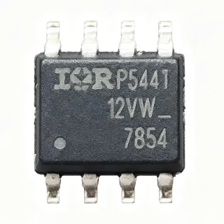
IRF7205PBF - -30V P-Channel HEXFET MOSFET, 4.6A, SO-8 | Infineon
料号: IRF7205PBF ✓ 量产中| 数量 | 单价 | 小计 |
|---|---|---|
| 1 | $0.97 | $0.97 |
| 10 | $0.85 | $8.50 |
| 100 | $0.72 | $72.00 |
| 500 | $0.61 | $305.00 |
| 1,000 | $0.54 | $540.00 |
| 3,000 | $0.47 | $1,410.00 |
IRF7205PBF 概述
A P-channel MOSFET is a voltage-controlled device in which the conducting channel is formed by p-type dopants between the source and drain. Because the channel turns on when the gate is pulled below the source potential, P-channel devices simplify high-side switching by eliminating the need for a boosted gate-drive supply. P-channel MOSFETs sit within the broader transistor family (P-MOSFET -> MOSFET -> discrete semiconductor -> power management) and are commonly used as load switches, battery isolation switches, and level shifters in portable, automotive, and industrial systems.
Key specifications of the IRF7205PBF include a gate threshold voltage typically around -1V to -3V, low gate charge for fast switching, and a planar cell structure that provides a wide safe operating area (SOA). The device is JEDEC-qualified and silicon-optimized for switching frequencies below 100 kHz, which covers most DC-DC converter and power-ORing applications. The ruggedized device design tolerates inductive switching transients, and the SO-8 footprint is one of the most widely adopted surface-mount power packages.
Typical applications include high-side load switching in notebook computers, USB power distribution, battery management systems, motor drive half-bridges (as the high-side switch), and hot-swap controllers. The -30V rating provides comfortable margin for 12V automotive rails and 19V laptop adapters, while the low on-resistance minimizes conduction loss.
When designing with this part, observe the SOA curve from the manufacturer datasheet and ensure that the maximum junction temperature of 150C is not exceeded under worst-case load and ambient conditions. Because P-channel turn-on requires VGS below ground, pay attention to gate-drive headroom, particularly in low-voltage systems below 5V. A gate resistor of 10-100 ohm is typically recommended to control ringing and EMI.
直接替换替代料: IRF7205PBF ——相同封装,引脚兼容。需要 PCB 改动的不同封装料号已排除。
本系列中的变体
可与以下型号直接替换的同系列型号: IRF7205PBF (相同外形与封装尺寸) ——差异在于 Technology, Operating Temperature Range, Package, Mounting Type, Drain-Source Voltage (VDS).
快速对比工具——选择替代料号进行并排对比:
IRF7422D2PBF
✅ 直接替换📋 参考替代料(不在目录中)
Si9407BDY
✅ 直接替换📋 参考替代料(不在目录中)
NTR4101PT1G
✅ 直接替换📋 参考替代料(不在目录中)
IRF7205PBF 最大额定值与电气特性
| Polarity | P-Channel |
| Drain-Source Voltage (VDS) | -30 V |
| Continuous Drain Current (ID) | -4.6 A |
| On-Resistance RDS(on) max at VGS=-10V | 70 mOhm |
| Gate Threshold Voltage VGS(th) | -1 V to -3 V (typical) |
| Technology | IR MOSFET (HEXFET, planar cell) |
| 封装 | SO-8 |
| 安装类型 | Surface Mount |
| 工作温度范围 | -55 C to +150 C (junction) |
| Switching Frequency Optimization | Below 100 kHz |
| Qualification | JEDEC standard |
| RoHS 状态 | Compliant (Pb-free per PBF suffix) |
| Generation | Fourth Generation HEXFET |
IRF7205PBF 引脚配置
| 引脚 1 | S — Source (internally connected to pins 2, 3) |
| 引脚 2 | S — Source (internally connected to pins 1, 3) |
| 引脚 3 | S — Source (internally connected to pins 1, 2) |
| 引脚 4 | G — Gate |
| 引脚 5 | D — Drain (internally connected to pins 6, 7, 8) |
| 引脚 6 | D — Drain (internally connected to pins 5, 7, 8) |
| 引脚 7 | D — Drain (internally connected to pins 5, 6, 8) |
| 引脚 8 | D — Drain (internally connected to pins 5, 6, 7) |
安全工作区
典型应用
IRF7205PBF 适用于 6 应用s: High-Side Load Switch, Notebook Computer Power Management, USB Power Distribution, Battery Isolation and Reverse Polarity Protection, Motor Drive Half-Bridge High-Side Switch, Industrial Switching and Hot-Swap.
High-Side Load Switch
The IRF7205PBF is ideal for high-side load switching in portable electronics because its P-channel structure eliminates the need for a boosted gate-drive supply. With VDS max of -30V and continuous drain current up to -4.6A, it cleanly switches 12V USB rails, LED strings, and peripheral power buses. The 70 mOhm RDS(on) at VGS = -10V keeps conduction loss below 1.5W at full load, while the JEDEC-qualified HEXFET process guarantees a wide SOA. Designers typically place the IRF7205PBF between the upstream regulator and the load, drive the gate from a logic-level GPIO through a 10-100 ohm resistor, and rely on its -30V rating to absorb inductive transients from cabling.
推荐
Notebook Computer Power Management
Inside notebook mainboards, the IRF7205PBF serves as a -30V-rated load switch on 19V adapter rails and battery isolation paths. Its fourth-generation HEXFET technology delivers 70 mOhm RDS(on), minimizing voltage drop and improving battery life when switching between AC adapter and battery sources. The SO-8 footprint drops directly onto existing layouts and handles the 4-5A peak currents typical of USB-PD and display backlight rails. Combined with a small gate pull-up resistor and TVS protection, the IRF7205PBF provides a compact, efficient power-MUX building block for ultrabook and tablet designs.
推荐
USB Power Distribution
The IRF7205PBF is widely used as the high-side switch in USB-A and USB-C VBUS distribution, where its P-channel topology lets a logic-level GPIO control 5V or 12V loads without a charge pump. The -30V VDS rating provides 2.5x safety margin over the 5V USB rail, tolerating ESD-coupled transients and cable-discharge events. The 4.6A continuous current rating comfortably delivers the 3A advertised by USB-PD, while the SO-8 package dissipates ~0.4W at full load without an external heatsink. Designers often pair the IRF7205PBF with a current-sense amplifier and an eFuse controller to build a compliant, hot-swappable USB port.
推荐
Battery Isolation and Reverse Polarity Protection
For battery isolation and reverse-polarity protection, the IRF7205PBF is configured as a high-side switch with its source tied to the battery positive terminal. Because the P-channel MOSFET is on when the gate is pulled to ground, a simple pulldown resistor keeps the system normally on, while a logic signal can override the gate for shutdown. Its -30V rating tolerates automotive load-dump pulses up to 35V when paired with a TVS, and the 70 mOhm on-resistance minimizes voltage drop across the isolation switch. SO-8 packaging and JEDEC qualification make the IRF7205PBF a robust choice for industrial and automotive battery systems.
推荐
Motor Drive Half-Bridge High-Side Switch
The IRF7205PBF functions as the high-side switch in small brushed-DC and stepper motor half-bridges for fans, pumps, and small actuators. Its -30V VDS rating suits 12V and 24V motor rails, while the planar-cell HEXFET structure provides a wide SOA to absorb back-EMF during commutation. The 4.6A continuous current supports motors up to approximately 30W without heatsinking. In a complementary half-bridge, the IRF7205PBF (P-channel high-side) is paired with an N-channel low-side MOSFET such as the BSS123NH6327XTSA1, driven through a bootstrap or gate-driver IC to achieve efficient PWM control at 25 kHz.
推荐
Industrial Switching and Hot-Swap
In industrial 24V systems and hot-swap controllers, the IRF7205PBF serves as the inrush-limiting element on plug-in cards and backplanes. Its -30V VDS rating comfortably exceeds the 24V industrial rail with headroom for transients, while the 70 mOhm RDS(on) limits steady-state dissipation. The wide SOA of the planar-cell HEXFET tolerates the simultaneous high-voltage and high-current conditions that occur during hot-plug events, allowing designers to simplify their hot-swap control loops. The SO-8 package and JEDEC qualification suit the rugged thermal and reliability requirements of factory automation, PLC I/O, and process-control instrumentation.
推荐
推荐产品汇总
工程参考数据: IRF7205PBF ——对比、设计指导和合规信息。
选型指南
与替代料对比
| 参数 | 本产品 | IRF7422D2PBF | IRFR024NTRPBF | Si9407BDY | NTR4101PT1G |
|---|---|---|---|---|---|
| Brand | Infineon | Infineon | Infineon | Vishay Intertechnology | onsemi |
| Package | SO-8 | SO-8 | DPAK (TO-252) | SO-8 | SO-8 |
| Polarity | P-Channel | P-Channel (dual) | P-Channel | P-Channel | P-Channel |
| VDS max | -30 V | -30 V | -55 V | -30 V | -30 V |
| Continuous Drain Current | -4.6 A | -2.6 A per channel | -17 A | -4.0 A | -3.7 A |
| RDS(on) max at VGS=-10V | 70 mOhm | 110 mOhm (per channel) | 75 mOhm | 100 mOhm | 80 mOhm |
| RoHS / Pb-Free | Yes (PBF suffix) | Yes (PBF suffix) | Yes (PBF suffix) | Yes | Yes |
| Single vs Dual P-Channel | Single | Dual | Single | Single | Single |
关键差异点
- Lower on-resistance than dual-channel alternative (对比 IRF7422D2PBF)
- Higher current rating than competing SO-8 P-channel (对比 NTR4101PT1G)
- Fourth-generation HEXFET process for low RDS(on) per area (对比 Si9407BDY)
设计说明
Estimated: at ID = 4.6A and RDS(on) = 70 mOhm, the IRF7205PBF dissipates approximately ID^2 x RDS(on) = 4.6^2 x 0.07 = 1.48W. On a 1 sq-in SO-8 copper pour (theta_JA ~50 C/W), junction temperature rises about 74C above ambient; at 85C ambient, TJ ~159C exceeds the 150C rating. Derate current to ~3A or enlarge the copper pour to 2 sq-in for reliable operation in enclosed enclosures.
Because pins 5-8 are the drain (which connects to the PCB tab and exposed copper on the SO-8 underside), maximize the drain copper pour to share heat between the package and the board. Keep the gate trace short and route it away from the drain switching node to minimize dv/dt-induced turn-on. A 10-100 ohm gate resistor damps ringing and limits peak gate current during fast transients.
Do not exceed VGS of +/-20V; the IRF7205PBF gate oxide can be permanently damaged by over-voltage. For high-side switching with a logic-level 3.3V or 5V GPIO, ensure VGS(th) is exceeded with margin - some IRF7205PBF samples show VGS(th) up to -3V, which may not fully enhance the MOSFET at VGS = -3.3V. Always use VGS = -10V for full enhancement unless a VGS(th)-derated variant is selected.
合规信息
The PBF suffix denotes lead-free (Pb-free) terminal finish compliant with EU RoHS. JEDEC qualified per Infineon datasheet. REACH and halogen-free status not explicitly stated in the verified web data.