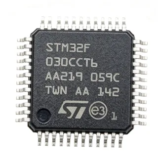
PIC16F722-I/SO - 8-Bit 20MHz Flash MCU, 3.5KB Flash, 28-SOIC | Microchip
料号: PIC16F722-I/SO ✓ 量产中PIC16F722-I/SO 概述
An 8-bit microcontroller is a complete computing core on a single chip: CPU, program memory, data memory, peripherals and I/O in one package. The PIC16 mid-range family sits between the tiny baseline parts and the larger PIC18/enhanced mid-range devices. It executes 35 single-word instructions on a 200 ns instruction cycle, uses a hardware stack 8 levels deep, and pairs that simple core with the low-power nanoWatt XLP feature set for sleep, watchdog and clock gating. In the wider hierarchy it is a microcontroller, then an embedded processor, then an integrated circuit and semiconductor.
Key features include on-chip Flash that can be programmed in-circuit, an internal 16 MHz oscillator that removes the need for an external crystal in most designs, and a peripheral set that includes I2C, SPI, AUSART (USART) and two CCP modules for capture, compare and PWM output. These features make it a compact controller for sensor nodes, actuator interfaces and small serial-bus systems without occupying a large PCB area.
Architecturally the device uses a Harvard-style RISC core with separate program and data memory spaces, so instruction fetch and data access proceed in parallel. The mid-range core is intentionally simple: 35 instructions, 8 hardware stack levels and a 200 ns execution time, which simplifies timing analysis for control loops and keeps interrupt handling predictable for time-sensitive control tasks.
Typical applications include industrial sensor and monitoring modules, low-power IoT and smart-home sensor nodes, battery-operated portable instruments, LED lighting and dimming controllers, small motor or relay control boards, and general-purpose serial-bridging or data-acquisition front ends where a UART, I2C and SPI are all needed on one part.
The key design consideration is decoupling and clock planning: fit the specified input and output bypass capacitors close to VDD and VSS pins, and route the MCLR/VPP programming and reset line away from switching nodes. Because the core is a 3.5 KB Flash part, firmware size planning matters as well; code built around the XLP sleep modes can extend battery life dramatically compared with a busy-wait design.
This page combines manufacturer and distributor documentation, drop-in replacement analysis for the same 28-pin SOIC footprint, side-by-side parameter comparison and practical layout guidance, giving engineers design context that a bare datasheet listing does not provide.
直接替换替代料: PIC16F722-I/SO ——相同封装,引脚兼容。需要 PCB 改动的不同封装料号已排除。
本系列中的变体
可与以下型号直接替换的同系列型号: PIC16F722-I/SO (相同外形与封装尺寸) ——差异在于 Package, ADC, Core, Timers, Family.
PIC16F723-I/SO
✅ 直接替换联系询价
查看数据手册 →PIC16F724-I/SO
✅ 直接替换 ⚠️ 规格未核验📋 参考替代料(不在目录中)
PIC16F726-I/SO
✅ 直接替换 ⚠️ 规格未核验联系询价
查看数据手册 →PIC16F727-I/SO
✅ 直接替换 ⚠️ 规格未核验📋 参考替代料(不在目录中)
PIC16F883-I/SO
✅ 直接替换 ⚠️ 规格未核验联系询价
查看数据手册 →PIC16F722-I/SO 最大额定值与电气特性
| Product Type | 8-bit RISC Flash Microcontroller (MCU) |
| Architecture | PIC16 mid-range core, 35 single-word instructions |
| Instruction Cycle Time | 200 ns |
| Maximum CPU Clock | 20 MHz |
| Internal Oscillator | 16 MHz internal |
| Program Memory (Flash) | 3.5 KB (2K x 14 words) |
| 封装 | 28-pin SOIC (SO-28), 0.50 mm pitch, surface mount |
| Supply Voltage Range | 2.5 V to 5.5 V |
| I/O Pins | 36 |
| Hardware Stack Depth | 8 levels |
| Serial Peripherals | I2C, SPI, AUSART (USART) |
| Timer/Capture Compare Modules | 2 x CCP (Capture/Compare/PWM) |
| Low Power Technology | nanoWatt XLP |
| Temperature Grade | Industrial (-I suffix) |
| 生命周期状态 | Active |
| Lead-Free Status | Lead-free plastic package |
| 安装类型 | Surface mount |
PIC16F722-I/SO 引脚配置
| 引脚 1 | RE3/MCLR/VPP — Programming / reset input (MCLR) and VPP, multiplexed with digital input RE3 |
| 引脚 2 | RA5/CLC1 — Port A digital I/O, also comparator output CLC1 |
| 引脚 3 | RE0/CLC2 — Port E digital I/O, also comparator output CLC2 |
| 引脚 4 | RA3/AN3 — Port A digital I/O, also analog input AN3 |
| 引脚 5 | RA2/AN2 — Port A digital I/O, also analog input AN2 |
| 引脚 6 | RA1/AN1 — Port A digital I/O, also analog input AN1 |
| 引脚 7 | RA0/AN0 — Port A digital I/O, also analog input AN0 |
| 引脚 8 | VSS — Ground reference for the analog and digital domains |
| 引脚 9 | RA7 — Port A digital I/O |
| 引脚 10 | RA6 — Port A digital I/O |
| 引脚 11 | RC0 — Port C digital I/O |
| 引脚 12 | RC1 — Port C digital I/O |
| 引脚 13 | RC2 — Port C digital I/O |
| 引脚 14 | RC3 — Port C digital I/O |
| 引脚 15 | RC4 — Port C digital I/O |
| 引脚 16 | RC5 — Port C digital I/O |
| 引脚 17 | RC6 — Port C digital I/O |
| 引脚 18 | RC7 — Port C digital I/O |
| 引脚 19 | VSS — Ground reference |
| 引脚 20 | VDD — Positive supply input for the digital domain |
| 引脚 21 | RB0/AN4 — Port B digital I/O, also analog input AN4 |
| 引脚 22 | RB1/AN5 — Port B digital I/O, also analog input AN5 |
| 引脚 23 | RB2 — Port B digital I/O |
| 引脚 24 | RB3 — Port B digital I/O |
| 引脚 25 | RB4 — Port B digital I/O |
| 引脚 26 | RB5 — Port B digital I/O |
| 引脚 27 | RB6 — Port B digital I/O |
| 引脚 28 | RB7 — Port B digital I/O |
典型应用
PIC16F722-I/SO 适用于 6 应用s: Industrial Sensor and Condition Monitoring, Low-Power IoT and Smart Home Sensor Nodes, LED Lighting and Dimming Control, Small Motor and Relay Control Boards, Portable Instrumentation and Data Acquisition, Serial Bridging and Protocol Conversion Hubs.
Industrial Sensor and Condition Monitoring
The PIC16F722-I/SO suits compact monitoring modules that read sensors and report results over a serial link. With I2C and SPI both on board, a single device can talk to digital temperature, humidity and pressure sensors over I2C while driving an SPI ADC or display. The 3.5 KB of Flash (2K x 14 words) holds the acquisition, filtering and communication routines, and the 20 MHz clock / 200 ns instruction cycle lets the firmware run periodic sampling loops with tight timing margins. The 28-pin SOIC package gives 36 I/O pins for discrete alarm outputs, status LEDs and sensor interrupt lines, while the 2.5 V to 5.5 V range lets the module sit on either a 3.3 V or 5 V industrial rail. nanoWatt XLP sleep modes are useful for battery-backed field units that sample at long intervals rather than continuously.
推荐
Low-Power IoT and Smart Home Sensor Nodes
Battery-operated IoT nodes benefit from the PIC16F722's combination of a small 28-pin SOIC footprint and the nanoWatt XLP low-power feature set. The 16 MHz internal oscillator removes the cost and area of an external crystal in designs that do not need the full 20 MHz operating point, while the 200 ns instruction cycle keeps reaction time short enough for duty-cycled wake, sample and transmit routines. I2C handles short-range sensor and EEPROM connections, and AUSART provides a simple uplink to a host or gateway over a UART bridge. The 2.5 V to 5.5 V supply range supports both coin-cell boosted rails and 3.3 V systems, and the -I industrial grade of the -I/SO variant suits indoor nodes subject to temperature swings. Firmware architecture should put the core to sleep between events and use watchdog recovery for unattended deployments.
推荐
LED Lighting and Dimming Control
The two CCP (Capture/Compare/PWM) modules on the PIC16F722-I/SO provide independent PWM outputs, which is exactly what constant-current LED drivers and dimming topologies require. A single PIC16F722 can generate a PWM dimming channel, capture a duty-cycle feedback signal from the LED driver, and manage fault signaling on spare I/O. The 20 MHz clock allows high-resolution PWM periods for flicker-free dimming and for driving MOSFET gates in boost or buck-boost LED converters. Its 3.5 KB Flash is enough for a state machine handling driver fault flags, thermal derating and minimum-brightness cutoff logic, while the wide 2.5 V to 5.5 V input tolerates both low-voltage battery strings and 5 V/12 V-referenced supplies after regulation. The SOIC-28 package is easy to route and to hand-solder in lighting modules.
推荐
Small Motor and Relay Control Boards
For stepper, solenoid and relay control, the PIC16F722-I/SO combines the mid-range core's fast 200 ns instruction cycle with two CCP modules and a hardware stack 8 levels deep, which keeps interrupt-driven control routines responsive. Timers can drive step-rate generation, while CCP outputs gate the MOSFET or driver stage; the AUSART accepts set-point commands from a host or panel. Thirty-six I/O pins in the 28-lead SOIC package leave ample room for limit switches, hall-effect inputs and fault flags. Because the Flash program memory is a modest 3.5 KB (2K x 14 words), motion profiles should be computed in RAM tables or offloaded to the host rather than stored as large look-up tables. The 2.5 V to 5.5 V supply range simplifies powering the logic from the same rail as the driver stage's low-side reference.
推荐
Portable Instrumentation and Data Acquisition
Battery-powered handheld instruments and small data-acquisition front ends need mixed signal capability with modest processing, and the PIC16F722-I/SO fits that profile. SPI connects to external ADCs and flash storage, I2C to sensors and calibration EEPROM, and AUSART to a host PC or a display controller. The 20 MHz clock with 200 ns instruction cycles supports averaging and filtering loops, and the on-board 16 MHz oscillator allows a cost-effective reference for timing and sample-rate generation without a crystal. The 28-pin SOIC footprint is compact enough for handheld enclosures and remains easy to hand-assemble for prototype runs. Because the -I/SO variant is the industrial temperature grade, the same board can be used in calibrated test equipment operating across factory and field temperatures, with the 2.5 V to 5.5 V range accepting either a lithium cell with boost or a 3.3 V regulated rail.
推荐
Serial Bridging and Protocol Conversion Hubs
Protocol-conversion and bridging nodes often need several serial interfaces in one small package, which is exactly where the PIC16F722-I/SO stands out. I2C, SPI and AUSART are all present, so the part can read sensors on an I2C bus, push data to SPI flash, and present a UART to a host processor. The mid-range core's 35-instruction set and 8-level stack keep interrupt servicing for three peripherals simple to reason about, and the 3.5 KB Flash holds protocol state machines without forcing an upgrade to a larger PIC. The 28-lead SOIC package with 36 I/O lines is easy to route into a small interface board, and the 2.5 V to 5.5 V range allows direct interfacing to 3.3 V logic or to 5 V legacy peripherals with level shifters only where required. The internal 16 MHz oscillator is adequate for most protocol timing, while an external clock can be fitted if baud-rate accuracy becomes critical.
推荐
推荐产品汇总
工程参考数据: PIC16F722-I/SO ——对比、设计指导和合规信息。
选型指南
与替代料对比
| 参数 | 本产品 | PIC16F723-I/SO | PIC16F724-I/SO | PIC16F726-I/SO | PIC16F727-I/SO | PIC16F883-I/SO |
|---|---|---|---|---|---|---|
| Brand | Microchip Technology | Microchip Technology | Microchip Technology | Microchip Technology | Microchip Technology | Microchip Technology |
| Package | SOIC-28 | SOIC-28 - same footprint | SOIC-28 - same footprint | SOIC-28 - same footprint | SOIC-28 - same footprint | SOIC-28 - same footprint |
| Maximum CPU Clock | 20 MHz | 20 MHz | 20 MHz | 20 MHz | 20 MHz | 20 MHz |
| Internal Oscillator | 16 MHz internal | 16 MHz internal | 16 MHz internal | 16 MHz internal | 16 MHz internal | Internal oscillator |
| Supply Voltage Range | 2.5 V to 5.5 V | 2.5 V to 5.5 V | 2.5 V to 5.5 V | 2.5 V to 5.5 V | 2.5 V to 5.5 V | 2.5 V to 5.5 V |
| Serial Peripherals | I2C, SPI, AUSART | I2C, SPI, AUSART | I2C, SPI, AUSART | I2C, SPI, AUSART | I2C, SPI, AUSART | I2C, SPI, AUSART |
| PWM / Capture Compare Modules | 2 x CCP | 2 x CCP | 2 x CCP | 2 x CCP | 2 x CCP | 2 x CCP |
| Low-Power Technology | nanoWatt XLP | nanoWatt XLP | nanoWatt XLP | nanoWatt XLP | nanoWatt XLP | nanoWatt XLP |
| Lifecycle Status | Active | Active | Active | Active | Active | Active |
关键差异点
- Three serial interfaces plus two PWM channels integrated on a 28-lead SOIC (对比 PIC16F883-I/SO)
- 20 MHz mid-range core with a 200 ns instruction cycle in a small SOIC-28 body (对比 PIC16F727-I/SO)
- Wide 2.5 V to 5.5 V operating range for both 3.3 V and 5 V rails (对比 PIC16F724-I/SO)
- nanoWatt XLP low-power feature set for duty-cycled and battery-operated nodes (对比 PIC16F723-I/SO)
设计说明
The PIC16F722-I/SO runs from a single 2.5 V to 5.5 V supply. Place the manufacturer-specified input bypass capacitor directly across VDD (pin 20) and VSS (pin 19), and add a second decoupling capacitor close to the IC if the board has long supply traces or switching sources nearby. Because the device exposes separate VDD and VSS pins at opposite ends of the 28-lead SOIC, route the ground return as a plane and keep the VDD/VSS pair short; excess supply inductance shows up as brown-out resets during PWM switching edges on adjacent drivers.
Keep the MCLR/VPP pin (pin 1) on a short, quiet trace. It is the programming and reset entry point, and capacitive coupling from adjacent switching nets can cause spurious resets in motor, LED or relay-drive designs. If MCLR is unused in the application, pull it up to VDD through the recommended resistor and avoid routing it near high dv/dt traces. For designs that use an external oscillator, keep the crystal or oscillator close to the oscillator pins and ground the associated caps to the quiet ground reference rather than to a switching return path.
The mid-range core is a 14-bit word architecture, so program memory is quoted as 3.5 KB (2K x 14 words) rather than 2048 bytes; writing firmware without accounting for this wastes a substantial portion of the available Flash. Check the compiler link settings and the actual map file for free space before adding features. Also verify peripheral pin multiplexing in the pin description table, because the family members share a footprint while assigning CCP, comparator and timer functions to different pins.
Estimated: for a design running at 3.3 V with a 5 mA average load, the PIC16F722-I/SO consumes roughly 16.5 mW of device power at the supply rail, excluding I/O drive current and external peripherals. That figure excludes the dominant standby losses, so on battery designs the XLP sleep-mode current, not the active current, usually sets the average consumption. Use sleep with peripheral interrupts for duty-cycled nodes and confirm the idle current in the Microchip electrical characteristics table before sizing the battery.
合规信息
The part is documented as a lead-free plastic package with a life cycle stage of ACTIVE. RoHS, REACH, halogen-free and conflict-minerals declarations are not stated in the available part documentation and must be confirmed with the manufacturer before use in regulated end equipment. The -I suffix denotes the industrial temperature grade; this is not an AEC-Q100 automotive-qualified variant.