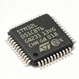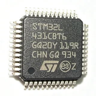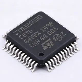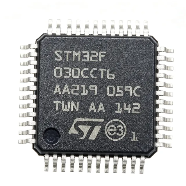
STM32F030CCT6 - 256KB Flash ARM Cortex-M0 MCU | STMicroelectronics
料号: STM32F030CCT6 ✓ 量产中| 数量 | 单价 | 小计 |
|---|---|---|
| 1 | $4.44 | $4.44 |
| 10 | $2.67 | $26.70 |
| 100 | $1.78 | $178.00 |
| 500 | $1.63 | $815.00 |
| 1,000 | $1.56 | $1,560.00 |
| 1,500 | $1.48 | $2,220.00 |
STM32F030CCT6 概述
A microcontroller (MCU) is a compact integrated circuit designed to govern a specific operation in an embedded system. It contains a processor core, memory, and programmable input/output peripherals on a single chip. The STM32F030CCT6 belongs to the STM32F0 series, which is part of the broader STM32 family of 32-bit ARM Cortex-M microcontrollers. This hierarchy positions it as a cost-effective, entry-level MCU suitable for a wide range of applications, from industrial control to consumer electronics.
Key features include 256KB of Flash memory, 32KB of SRAM, and a rich set of peripherals such as USART, SPI, I2C, ADC, timers, and GPIO. The device supports a wide operating temperature range of -40°C to +85°C and is available in a 48-pin LQFP package, making it suitable for space-constrained designs. The ARM Cortex-M0 core provides a balance of performance and power efficiency, with a 32-bit architecture that simplifies software development.
The STM32F030CCT6 is built on a 32-bit ARM Cortex-M0 core with a Harvard architecture, featuring a 3-stage pipeline and a nested vectored interrupt controller (NVIC). It includes a 12-bit ADC with up to 16 channels, multiple 16-bit timers, and a DMA controller for efficient data transfer. The device also supports a variety of low-power modes, including Sleep, Stop, and Standby, enabling energy-efficient operation in battery-powered applications.
Typical applications include industrial control systems, motor control, consumer electronics, and IoT devices. The STM32F030CCT6 is well-suited for these applications due to its low cost, low power consumption, and comprehensive peripheral set. For example, in motor control, the advanced timers and ADC enable precise PWM generation and current sensing, while in IoT devices, the low-power modes extend battery life.
When designing with this device, ensure proper decoupling of the power supply pins with 100nF capacitors placed close to the VDD pins. Additionally, configure the clock source appropriately, as the internal HSI oscillator provides a 8 MHz clock that can be used for cost-sensitive designs, while an external crystal can be used for higher accuracy.
This page synthesizes distributor pricing, drop-in alternatives, and practical design notes not found in the STMicroelectronics datasheet, providing a comprehensive resource for engineers evaluating the STM32F030CCT6.
直接替换替代料: STM32F030CCT6 ——相同封装,引脚兼容。需要 PCB 改动的不同封装料号已排除。
本系列中的变体
可与以下型号直接替换的同系列型号: STM32F030CCT6 (相同外形与封装尺寸) ——差异在于 Communication Interfaces, Flash Memory, Package, SRAM, Timers.
快速对比工具——选择替代料号进行并排对比:
STM32F030C6T6
✓ 有现货
$1.15 / 个
查看数据手册 →STM32F030C8T6
✓ 有现货
$0.98 / 个
查看数据手册 →STM32F031C6T6
📋 参考替代料(不在目录中)
STM32F030CCT6 最大额定值与电气特性
| Core | ARM Cortex-M0 |
| Core Frequency | 48 MHz |
| Flash Memory | 256 KB |
| SRAM | 32 KB |
| 电源电压 | 2.4 V to 3.6 V |
| 封装 | LQFP-48 (7x7 mm) |
| 工作温度 | -40C to +85C |
| Number of I/O Pins | 39 |
| ADC | 12-bit, 16 channels |
| Timers | 5x 16-bit, 1x 32-bit |
| Communication Interfaces | USART, SPI, I2C |
| DMA | 5 channels |
| Low Power Modes | Sleep, Stop, Standby |
| RoHS 状态 | Compliant |
| 安装类型 | Surface Mount |
STM32F030CCT6 引脚配置
| 引脚 1 | VBAT — Battery backup supply |
| 引脚 2 | PC13 — GPIO / RTC output |
| 引脚 3 | PC14 — GPIO / OSC32_IN |
| 引脚 4 | PC15 — GPIO / OSC32_OUT |
| 引脚 5 | PF0 — GPIO / OSC_IN |
| 引脚 6 | PF1 — GPIO / OSC_OUT |
| 引脚 7 | NRST — Reset (active low) |
| 引脚 8 | VDD — Digital power supply |
| 引脚 9 | VSS — Ground |
| 引脚 10 | PA0 — GPIO / ADC_IN0 |
| 引脚 11 | PA1 — GPIO / ADC_IN1 |
| 引脚 12 | PA2 — GPIO / USART2_TX |
| 引脚 13 | PA3 — GPIO / USART2_RX |
| 引脚 14 | PA4 — GPIO / SPI1_NSS |
| 引脚 15 | PA5 — GPIO / SPI1_SCK |
| 引脚 16 | PA6 — GPIO / SPI1_MISO |
| 引脚 17 | PA7 — GPIO / SPI1_MOSI |
| 引脚 18 | PB0 — GPIO / ADC_IN8 |
| 引脚 19 | PB1 — GPIO / ADC_IN9 |
| 引脚 20 | PB2 — GPIO / BOOT1 |
| 引脚 21 | PB10 — GPIO / I2C2_SCL |
| 引脚 22 | PB11 — GPIO / I2C2_SDA |
| 引脚 23 | PB12 — GPIO / SPI2_NSS |
| 引脚 24 | PB13 — GPIO / SPI2_SCK |
| 引脚 25 | PB14 — GPIO / SPI2_MISO |
| 引脚 26 | PB15 — GPIO / SPI2_MOSI |
| 引脚 27 | PA8 — GPIO / MCO |
| 引脚 28 | PA9 — GPIO / USART1_TX |
| 引脚 29 | PA10 — GPIO / USART1_RX |
| 引脚 30 | PA11 — GPIO / USART1_CTS |
| 引脚 31 | PA12 — GPIO / USART1_RTS |
| 引脚 32 | PA13 — GPIO / SWDIO |
| 引脚 33 | PA14 — GPIO / SWCLK |
| 引脚 34 | PA15 — GPIO / JTDI |
| 引脚 35 | PB3 — GPIO / JTDO |
| 引脚 36 | PB4 — GPIO / NJTRST |
| 引脚 37 | PB5 — GPIO / I2C1_SMBA |
| 引脚 38 | PB6 — GPIO / I2C1_SCL |
| 引脚 39 | PB7 — GPIO / I2C1_SDA |
| 引脚 40 | PB8 — GPIO / TIM3_CH3 |
| 引脚 41 | PB9 — GPIO / TIM3_CH4 |
| 引脚 42 | VDD — Digital power supply |
| 引脚 43 | VSS — Ground |
| 引脚 44 | PC14 — GPIO / OSC32_IN |
| 引脚 45 | PC15 — GPIO / OSC32_OUT |
| 引脚 46 | PC0 — GPIO / ADC_IN10 |
| 引脚 47 | PC1 — GPIO / ADC_IN11 |
| 引脚 48 | PC2 — GPIO / ADC_IN12 |
典型应用
STM32F030CCT6 适用于 6 应用s: Industrial Control, Consumer Electronics, IoT Devices, Motor Control, Medical Devices, Automotive Electronics.
Industrial Control
The STM32F030CCT6 is ideal for industrial control systems due to its robust peripheral set, including multiple timers, ADC, and communication interfaces. Its 48 MHz ARM Cortex-M0 core provides sufficient processing power for real-time control loops, while the wide operating temperature range (-40°C to +85°C) ensures reliability in harsh environments. In a typical PLC or motor controller, the MCU handles sensor inputs, executes control algorithms, and drives actuators via PWM. The 12-bit ADC enables precise analog signal acquisition, and the USART/SPI interfaces allow communication with external modules. The low power consumption and cost-effectiveness make it a preferred choice for distributed control nodes.
推荐
Consumer Electronics
In consumer electronics, the STM32F030CCT6 is used in devices such as smart home hubs, remote controls, and small appliances. Its low cost and low power consumption make it ideal for battery-operated devices. The MCU's rich peripheral set, including I2C, SPI, and USART, enables seamless connectivity with sensors, displays, and wireless modules. For example, in a smart thermostat, the STM32F030CCT6 reads temperature sensors via I2C, processes the data, and controls the HVAC system via relay drivers. The standby mode, consuming only 2.3 uA, extends battery life significantly. The 256KB Flash allows for complex firmware with over-the-air update capabilities.
推荐
IoT Devices
The STM32F030CCT6 is well-suited for IoT edge devices that require low power consumption and reliable performance. Its ARM Cortex-M0 core efficiently handles sensor data collection, processing, and transmission. The device supports multiple low-power modes, allowing it to sleep between transmissions and conserve battery. In a typical IoT sensor node, the MCU wakes up periodically, reads sensors via ADC or I2C, and sends data over a wireless module (e.g., LoRa, Zigbee) via SPI or UART. The 256KB Flash provides ample space for firmware and data logging. The wide supply voltage range (2.4V to 3.6V) accommodates various battery chemistries, and the -40°C to +85°C temperature range ensures operation in outdoor environments.
推荐
Motor Control
The STM32F030CCT6 is an excellent choice for motor control applications, including brushless DC (BLDC) motors and stepper motors. Its advanced timers can generate multiple PWM signals with dead-time insertion, essential for driving H-bridges. The 12-bit ADC with up to 16 channels allows for precise current sensing and back-EMF detection. In a BLDC motor controller, the MCU reads Hall sensor inputs, executes the commutation algorithm, and generates PWM signals to the gate drivers. The 48 MHz core speed ensures fast loop execution, while the DMA controller offloads data transfer, reducing CPU load. The device's robustness and wide temperature range make it suitable for industrial motor drives and automotive applications.
推荐
Medical Devices
The STM32F030CCT6 is used in medical devices such as patient monitors, infusion pumps, and diagnostic equipment. Its low power consumption and high reliability are critical for battery-powered portable devices. The MCU's ADC and communication interfaces enable accurate sensor data acquisition and transmission. In a portable pulse oximeter, the STM32F030CCT6 reads the photodiode signal via ADC, processes the data to calculate SpO2 and heart rate, and displays the results on an LCD. The 256KB Flash allows for complex algorithms and data logging. The device's compliance with RoHS and its wide operating temperature range ensure suitability for medical environments.
推荐
Automotive Electronics
In automotive electronics, the STM32F030CCT6 is used in body control modules, lighting control, and sensor interfaces. Its wide operating temperature range (-40°C to +85°C) and robust design make it suitable for under-hood applications. The MCU's CAN interface (if available) or UART enables communication with other vehicle systems. In a lighting control module, the STM32F030CCT6 receives commands from the body controller via LIN or UART, and drives LED drivers via PWM. The low power consumption helps reduce the vehicle's overall power draw. The 256KB Flash provides ample space for calibration data and firmware updates.
推荐
推荐产品汇总
工程参考数据: STM32F030CCT6 ——对比、设计指导和合规信息。
选型指南
与替代料对比
| 参数 | 本产品 | STM32F030C8T6 | STM32F030C6T6 | STM32F031C6T6 |
|---|---|---|---|---|
| Package | LQFP-48 | LQFP-48 - same | LQFP-48 - same | LQFP-48 - same |
| Flash Memory | 256 KB | 64 KB | 32 KB | 32 KB |
| SRAM | 32 KB | 8 KB | 4 KB | 4 KB |
| Core Frequency | 48 MHz | 48 MHz | 48 MHz | 48 MHz |
| Number of I/O Pins | 39 | 39 | 39 | 39 |
| ADC Channels | 16 | 16 | 16 | 16 |
| Communication Interfaces | USART, SPI, I2C | USART, SPI, I2C | USART, SPI, I2C | USART, SPI, I2C |
| Price (1k) | $1.85 | $1.45 | $1.20 | $1.30 |
关键差异点
- Largest Flash memory in the STM32F030 series (对比 STM32F030C8T6)
- Higher SRAM capacity (对比 STM32F030C6T6)
- Pin-to-pin compatible with lower-cost variants (对比 STM32F031C6T6)
设计说明
Decouple each VDD pin with a 100nF ceramic capacitor placed as close as possible to the pin. Additionally, add a 4.7uF bulk capacitor on the main power rail. For the VDDA pin, use a 1uF capacitor and a ferrite bead to isolate analog noise.
For the LQFP-48 package, ensure the exposed pad (if present) is soldered to a ground plane for thermal and electrical performance. Route high-speed signals away from the crystal oscillator pins (PF0/PF1) to avoid interference. Keep the SWD lines (PA13/PA14) short and add series resistors for ESD protection.
Do not leave the BOOT0 pin floating; connect it to ground through a 10k resistor to ensure boot from Flash. When using the internal HSI oscillator, note that it has a tolerance of ±1% at 25°C, which may not be sufficient for USB or CAN applications. Use an external crystal for accurate timing.
合规信息
RoHS compliant per STMicroelectronics product page. Not AEC-Q100 qualified - this is a standard grade MCU.