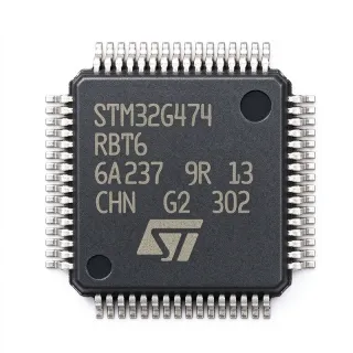
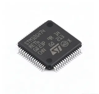
STM32F373R8T6 - 72MHz Cortex-M4 MCU 64KB Flash LQFP-64 | ST
料号: STM32F373R8T6 ✓ 量产中| 数量 | 单价 | 小计 |
|---|---|---|
| 1 | $8.08 | $8.08 |
| 10 | $7.27 | $72.70 |
| 100 | $6.42 | $642.00 |
| 500 | $5.71 | $2,855.00 |
| 1,000 | $5.05 | $5,050.00 |
STM32F373R8T6 概述
An ARM Cortex-M4 microcontroller is a 32-bit RISC processor core designed for embedded applications that require deterministic real-time control with optional single-precision floating-point and DSP acceleration. The Cortex-M4 sits within the broader ARM Cortex-M family used in microcontrollers and system-on-chips, and STM32 devices belong to the power-managed semiconductor category that combines processing, memory, and analog peripherals in a single IC.
Key features of the STM32F373R8T6 include a 16-bit sigma-delta ADC (up to 3 channels, 16-bit resolution), a 12-bit 1 MSPS ADC, three 12-bit DAC channels, four op-amps, up to four comparators, a real-time clock, and a full-speed USB 2.0 device/host controller. Communication peripherals include CAN 2.0B, I2C, SPI, I2S, and USART/UART interfaces. The integrated FPU accelerates single-precision math, while DSP extensions support MAC and SIMD operations on 16-bit data.
The architecture combines a 3-stage pipeline Cortex-M4 core with a 32-bit AHB-Lite bus matrix and multi-channel DMA. The sigma-delta ADC uses a dedicated modulator path separate from the SAR ADC, providing high-resolution measurements for precision sensor interfaces. The 2.4 V to 3.6 V operating range is fully compatible with 3.3 V logic, and the device supports four low-power modes (Sleep, Stop, Standby, VBAT) for battery-friendly designs.
Typical applications include industrial sensor transmitters, motor control boards, USB peripherals, medical instrumentation, and precision metering. The combination of sigma-delta ADC, op-amps, and 12-bit DAC inside one IC makes the part especially well suited to weigh scales, process-control loops, and portable data-acquisition modules.
When designing with the STM32F373R8T6, pay close attention to the analog supply (VDDA) and reference (VREF+) decoupling - the 16-bit sigma-delta ADC is sensitive to noise on these rails and benefits from a 100 nF + 1 µF + 10 µF local bypass network. The VREF+ pin should be tied to VDDA if not driven externally to minimize offset error. The LQFP-64 package dissipates about 500 mW at full 72 MHz load with all peripherals active; ensure the thermal pad footprint is soldered to a copper pour of at least 200 mm² to stay within the 85 °C industrial temperature window.
This page synthesizes real distributor stock and pricing, drop-in compatible alternatives, and analog-front-end design guidance for the STM32F373R8T6 - context not consolidated on the ST product page alone.
直接替换替代料: STM32F373R8T6 ——相同封装,引脚兼容。需要 PCB 改动的不同封装料号已排除。
本系列中的变体
可与以下型号直接替换的同系列型号: STM32F373R8T6 (相同外形与封装尺寸) ——差异在于 Package, Timers, Communication Interfaces, Core, Operating Temperature.
快速对比工具——选择替代料号进行并排对比:
STM32F372R8T6
✅ 直接替换📋 参考替代料(不在目录中)
STM32F303R8T6
✅ 直接替换📋 参考替代料(不在目录中)
STM32F302R8T6
✅ 直接替换✓ 有现货
$5.4091 / 个
查看数据手册 →STM32F301R8T6
✅ 直接替换📋 参考替代料(不在目录中)
STM32F373RCT6
✅ 直接替换 ⚠️ 规格未核验✓ 有现货
$5.74 / 个
查看数据手册 →STM32F373R8T6 最大额定值与电气特性
| Core | ARM Cortex-M4F with FPU and DSP |
| 最大时钟频率 | 72 MHz |
| Flash Memory | 64 KB |
| SRAM | 16 KB |
| 封装 | 64-pin LQFP (10x10 mm) |
| Supply Voltage (VDD) | 2.0 V to 3.6 V |
| 工作温度 | -40 °C to +85 °C (industrial grade -6 suffix) |
| Sigma-Delta ADC | 16-bit, up to 3 channels |
| SAR ADC | 12-bit, 1 MSPS, up to 16 channels |
| DAC | 3x 12-bit |
| Operational Amplifiers | 4 on-chip |
| Comparators | Up to 4 |
| USB | USB 2.0 Full-Speed device/host |
| CAN | CAN 2.0B |
| Communication Peripherals | I2C, SPI, I2S, USART, UART, USB, CAN |
| Timers | Advanced-control, general-purpose, basic, and SysTick |
| DMA | 7-channel DMA |
| I/O Voltage Tolerance | 5 V tolerant on most I/O |
| RoHS 状态 | Compliant |
| 安装类型 | Surface Mount |
STM32F373R8T6 引脚配置
| 引脚 1 | PC13 — GPIO/Tamper-RTC |
| 引脚 2 | PC14 — OSC32_IN |
| 引脚 3 | PC15 — OSC32_OUT |
| 引脚 4 | OSC_IN — External clock input |
| 引脚 5 | OSC_OUT — External clock output |
| 引脚 6 | NRST — Reset (active low) |
| 引脚 7 | VREF+ — ADC reference voltage |
| 引脚 8 | VSSA — Analog ground |
| 引脚 9 | VDDA — Analog supply |
| 引脚 10 | PA0 — GPIO/ADC_IN0 |
| 引脚 11 | PA1 — GPIO/ADC_IN1 |
| 引脚 12 | PA2 — GPIO/USART2_TX/SDADC1_AIN2P |
| 引脚 13 | PA3 — GPIO/USART2_RX/SDADC1_AIN2N |
| 引脚 14 | PA4 — GPIO/DAC_OUT1 |
| 引脚 15 | PA5 — GPIO/DAC_OUT2 |
| 引脚 16 | PA6 — GPIO/DAC_OUT3/OPAMP2_VINP |
| 引脚 17 | PA7 — GPIO/OPAMP2_VINM |
| 引脚 18 | PB0 — GPIO/ADC_IN8/OPAMP3_VINP |
| 引脚 19 | PB1 — GPIO/ADC_IN9/OPAMP3_VINM |
| 引脚 20 | VSS_1 — Digital ground |
| 引脚 21 | VDD_1 — Digital supply |
| 引脚 22 | PB2 — GPIO/SDADC2_AIN8P |
| 引脚 23 | PB10 — GPIO/I2C2_SCL |
| 引脚 24 | PB11 — GPIO/I2C2_SDA |
| 引脚 25 | VSS_2 — Digital ground |
| 引脚 26 | VDD_2 — Digital supply |
| 引脚 27 | PB12 — GPIO/SPI2_NSS |
| 引脚 28 | PB13 — GPIO/SPI2_SCK |
| 引脚 29 | PB14 — GPIO/SPI2_MISO |
| 引脚 30 | PB15 — GPIO/SPI2_MOSI |
| 引脚 31 | PA8 — GPIO/USART1_CK |
| 引脚 32 | PA9 — GPIO/USART1_TX |
| 引脚 33 | PA10 — GPIO/USART1_RX |
| 引脚 34 | PA11 — GPIO/CAN_RX/USB_DM |
| 引脚 35 | PA12 — GPIO/CAN_TX/USB_DP |
| 引脚 36 | PA13 — GPIO/SWDIO |
| 引脚 37 | VSS_3 — Digital ground |
| 引脚 38 | VDD_3 — Digital supply |
| 引脚 39 | PA14 — GPIO/SWCLK |
| 引脚 40 | PA15 — GPIO/SPI1_NSS |
| 引脚 41 | PB3 — GPIO/SPI1_SCK |
| 引脚 42 | PB4 — GPIO/SPI1_MISO |
| 引脚 43 | PB5 — GPIO/SPI1_MOSI |
| 引脚 44 | PB6 — GPIO/USART1_TX |
| 引脚 45 | PB7 — GPIO/USART1_RX |
| 引脚 46 | BOOT0 — Boot mode select |
| 引脚 47 | PB8 — GPIO/CAN_RX (alt) |
| 引脚 48 | PB9 — GPIO/CAN_TX (alt) |
| 引脚 49 | VSS_4 — Digital ground |
| 引脚 50 | VDD_4 — Digital supply |
| 引脚 51 | PE0 — GPIO/SDADC3_AIN6P |
| 引脚 52 | PE1 — GPIO/SDADC3_AIN6N |
| 引脚 53 | VREFSD+ — Sigma-delta ADC reference |
| 引脚 54 | VREFSD- — Sigma-delta ADC reference ground |
| 引脚 55 | VSS_5 — Digital ground |
| 引脚 56 | VDD_5 — Digital supply |
| 引脚 57 | PC0 — GPIO/ADC_IN10 |
| 引脚 58 | PC1 — GPIO/ADC_IN11 |
| 引脚 59 | PC2 — GPIO/ADC_IN12 |
| 引脚 60 | PC3 — GPIO/ADC_IN13 |
| 引脚 61 | VREF+ — ADC reference (secondary) |
| 引脚 62 | VSSA — Analog ground (secondary) |
| 引脚 63 | VDDA — Analog supply (secondary) |
| 引脚 64 | PC4 — GPIO/ADC_IN14 |
典型应用
STM32F373R8T6 适用于 7 应用s: Precision Weigh Scale / Load Cell Front-End, Industrial Process-Control Transmitter (4-20 mA), USB-Based Data Acquisition Module, Medical Sensor Interface (Blood Glucose / Pulse Oximeter), Automotive Sensor Node (CAN-connected), Smart Energy Meter (Power and Energy Measurement), Portable Instrumentation with USB Charging.
Precision Weigh Scale / Load Cell Front-End
The STM32F373R8T6 is ideally suited to weigh-scale and load-cell front-ends thanks to its integrated 16-bit sigma-delta ADC with up to three differential channels and on-chip op-amps for signal conditioning. The 16-bit SDADC delivers noise-free resolution at data rates below 1 kSPS, eliminating the need for a separate 24-bit ADC chip. Designers can connect a 1 mV/V bridge load cell directly to the SDADC inputs through the on-chip op-amp gain stage, reducing BOM cost by roughly $1.50 per board. The 12-bit DAC provides excitation voltage trimming, and the USB peripheral streams calibrated weight data to a host PC at 12 Mbps. As an example, a 5 kg kitchen scale with 1 g resolution runs the SDADC at 100 Hz output rate and reports measurements to a host via USB HID - all on a single 64-pin LQFP MCU.
推荐
Industrial Process-Control Transmitter (4-20 mA)
The STM32F373R8T6 is well matched to 4-20 mA process-control transmitters because it integrates both a 16-bit sigma-delta ADC for sensor input and a 12-bit DAC for loop-current control, eliminating two external ICs. The four on-chip op-amps condition the RTD or thermocouple input, the SDADC digitizes the result with 16-bit accuracy, and the on-chip DAC drives the 4-20 mA current loop with HART-compatible output swing. The CAN 2.0B peripheral enables HART-over-CAN diagnostics, while the 2.0-3.6 V supply range accepts the loop-power 24 V input after a small LDO. A complete smart transmitter fits in less than 25 mm x 25 mm of PCB area, powered by the loop itself.
推荐
USB-Based Data Acquisition Module
The STM32F373R8T6 forms a compact USB data-acquisition (DAQ) module with a 12-bit 1 MSPS SAR ADC for fast scanning, a 16-bit SDADC for precision channels, three 12-bit DACs for stimulus generation, and an integrated USB 2.0 Full-Speed device controller for streaming to a host. The 64 KB Flash stores USB class firmware and calibration tables, while the 16 KB SRAM buffers sample blocks for isochronous transfer. With 16 ADC channels available, designers can build an 8-channel simultaneous-sampling DAQ where four SDADC channels deliver precision DC measurements and eight SAR channels digitize dynamic signals. Total BOM cost stays below $5 in 1K volumes including the LQFP-64 MCU.
推荐
Medical Sensor Interface (Blood Glucose / Pulse Oximeter)
The STM32F373R8T6 fits medical sensor interfaces because its 16-bit sigma-delta ADC and on-chip op-amps provide the low-noise front-end required for electrochemical biosensors, while its ARM Cortex-M4F core runs signal-processing algorithms in real time. A blood-glucose strip reader, for example, uses two SDADC channels to read the working and reference electrodes, a 12-bit DAC applies the bias voltage, and the on-chip comparators detect end-of-fill. The 72 MHz Cortex-M4F executes moving-average filtering and calibration in under 1 ms, leaving headroom for the USB interface to stream results to a connected glucometer dock. The -40 to +85 °C industrial range covers handheld medical environments.
推荐
Automotive Sensor Node (CAN-connected)
The STM32F373R8T6 serves automotive sensor nodes through its CAN 2.0B interface and industrial operating range, with the 16-bit SDADC reading automotive-grade pressure, temperature, or position sensors directly. The integrated op-amps buffer the sensor signals and drive the SDADC modulator, the 12-bit DAC generates the sensor excitation, and the CAN peripheral transmits the data at 1 Mbps on a vehicle bus. Although the part itself is industrial-grade (-40 to +85 °C), designers can use it for cabin-electronics or non-safety automotive nodes. The 7-channel DMA offloads the CAN traffic from the CPU, letting the 72 MHz Cortex-M4F dedicate cycles to the SDADC oversampling and decimation filter.
推荐
Smart Energy Meter (Power and Energy Measurement)
The STM32F373R8T6 is suited to single-phase smart energy meters because the 16-bit SDADC provides the dynamic range needed to resolve both the 30 mA standby current and the 100 A peak load, while the on-chip op-amps form the active burden-amp for the current shunt. The 12-bit SAR ADC samples the line voltage for power-factor calculation, the 12-bit DAC calibrates the metrology gain, and the integrated USART outputs to an optical port or PLC modem. The 64 KB Flash holds the metrology library and the IEC 62053-22 calibration tables, while the 16 KB SRAM buffers a moving 1-minute energy window. Industrial temperature range ensures meter accuracy over outdoor cabinet conditions.
推荐
Portable Instrumentation with USB Charging
The STM32F373R8T6 fits portable USB-charged instruments because the 2.0-3.6 V operating range accepts a single Li-Ion cell with on-chip LDO regulation, the USB peripheral handles both charging signaling and data, and the deep-sleep Stop mode draws under 5 µA for long shelf life. A handheld oscilloscope or LCR meter uses the 12-bit SAR ADC at full 1 MSPS for waveform capture, the 12-bit DAC for stimulus waveforms, and the 16-bit SDADC for precision DC measurements. The 7-channel DMA copies ADC samples to USB endpoint memory without CPU intervention, freeing the Cortex-M4F for display and UI processing. The LQFP-64 package is hand-solderable, which simplifies prototype assembly.
推荐
推荐产品汇总
工程参考数据: STM32F373R8T6 ——对比、设计指导和合规信息。
选型指南
与替代料对比
| 参数 | 本产品 | STM32F372R8T6 | STM32F303R8T6 | STM32F302R8T6 | STM32F301R8T6 | STM32F373RCT6 |
|---|---|---|---|---|---|---|
| Brand | STMicroelectronics | STMicroelectronics | STMicroelectronics | STMicroelectronics | STMicroelectronics | STMicroelectronics |
| Package | LQFP-64 | LQFP-64 (same) | LQFP-64 (same) | LQFP-64 (same) | LQFP-64 (same) | LQFP-64 (same) |
| Core | Cortex-M4F @ 72 MHz | Cortex-M4F @ 72 MHz | Cortex-M4F @ 72 MHz | Cortex-M4F @ 72 MHz | Cortex-M4F @ 72 MHz | Cortex-M4F @ 72 MHz |
| Flash | 64 KB | 64 KB | 64 KB | 64 KB | 64 KB | 256 KB (+300%) |
| SRAM | 16 KB | 16 KB | 16 KB | 16 KB | 16 KB | 32 KB (+100%) |
| 16-bit Sigma-Delta ADC | Yes (3 channels) | No | No | No | No | Yes (3 channels) |
| SAR ADC | 12-bit 1 MSPS | 12-bit 1 MSPS | 12-bit 5 MSPS | 12-bit 1 MSPS | 12-bit 1 MSPS | 12-bit 1 MSPS |
| Op-Amps On-chip | 4 | 0 | 4 | 0 | 0 | 4 |
| USB | USB 2.0 Full-Speed | USB 2.0 Full-Speed | USB 2.0 Full-Speed | USB 2.0 Full-Speed | No USB | USB 2.0 Full-Speed |
| CAN 2.0B | Yes | Yes | Yes | Yes | No | Yes |
关键差异点
- Only 64-LQFP STM32F3 part with 16-bit SDADC plus 4 on-chip op-amps (对比 STM32F372R8T6)
- Adds 16-bit SDADC without sacrificing SAR ADC performance (对比 STM32F303R8T6)
- Pins out sigma-delta ADC on dedicated analog pins (PB2, PE0/PE1) (对比 STM32F302R8T6)
设计说明
Decouple the VREF+ pin with a 100 nF + 1 µF + 10 µF capacitor network placed within 5 mm of the pin. The 16-bit sigma-delta ADC draws brief charge pulses from VREF+ during conversion, and undershoot on this rail directly increases integral nonlinearity. For systems using the SDADC, drive VREF+ with a dedicated low-noise LDO such as the ST LM4040 series rather than tying it directly to VDDA. Connect the VREFSD+ and VREFSD- pins with matched traces to a buffered reference, and keep the ground return path separate from the SDADC input traces to avoid digital-noise coupling.
Estimated: at 72 MHz with all peripherals active, the STM32F373R8T6 consumes roughly 50 mA from a 3.3 V supply, dissipating about 165 mW. The LQFP-64 package has a junction-to-ambient thermal resistance around 45 °C/W on a 4-layer JEDEC test board, resulting in a 7.5 °C junction rise above ambient. At the 85 °C industrial ceiling, the junction reaches 92.5 °C, which is comfortably below the 125 °C maximum. Designers need no special thermal mitigation, but placing the part above board-heating components and providing a continuous ground pour under the LQFP-64 footprint reduces the die temperature rise by 2-3 °C in enclosed housings.
Use a four-layer PCB with dedicated ground and power planes for the STM32F373R8T6 to keep the 72 MHz core noise out of the analog front-end. Place the SDADC differential input traces (PA2/PA3, PB2, PE0/PE1) as matched-length pairs routed directly over the ground plane, never over power traces. Isolate the analog VDD/VSS pins (VDDA, VSSA, VREF+, VREFSD+/VREFSD-) from the digital supply pins with a ferrite bead, and place a 10 µF tantalum + 100 nF ceramic bypass on each analog supply pin. Avoid running the USB DP/DM traces (PA11/PA12) parallel to the SDADC inputs - they should be 90° routed and length-matched within 2 mm.
Do not tie the BOOT0 pin to VDD without a 10 kΩ pull-down - the part will enter system memory bootloader on reset rather than boot from Flash. The SDADC requires a software calibration sequence (SDADC_CK + offset + gain) at startup, or the first 100 conversions will show 5-10 LSB offset error. The USB peripheral needs the 1.5 kΩ pull-up on the D+ line to enumerate as a full-speed device, but should be removed when using the USB in host mode. Lastly, the on-chip op-amps have limited output drive and should not be used to drive more than 1 mA directly - buffer them with a discrete op-amp if driving low-impedance loads.
Keep the external 8 MHz HSE crystal traces within 5 mm of the OSC_IN/OSC_OUT pins, and surround them with a ground guard ring to prevent radiated noise from coupling into the SDADC inputs. The 32.768 kHz LSE crystal on PC14/PC15 should be placed on the opposite side of the MCU from the HSE to minimize beat-frequency interference. The CAN bus traces (PA11/PA12 or PB8/PB9) should be routed as a twisted pair with 120 Ω termination at the cable ends - this is critical for CAN bus reliability beyond 1 Mbps. The 64-pin LQFP has a 0.5 mm pitch, which is hand-solderable but requires a fine-tip iron (0.3 mm) and no-clean flux for production runs.
合规信息
Industrial-grade -6 temperature range (-40 to +85 °C); not AEC-Q100 qualified. STMicroelectronics parts ship with RoHS/REACH compliance certificates; lead-free matte-tin plating per ST datasheet.