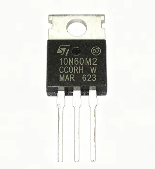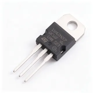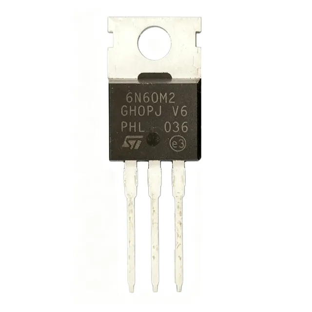
STP6N60M2 - 600V 5A N-Channel Power MOSFET | STMicroelectronics
料号: STP6N60M2 ✓ 量产中| 数量 | 单价 | 小计 |
|---|---|---|
| 1 | $0.8182 | $0.82 |
| 10 | $0.5909 | $5.91 |
| 100 | $0.5227 | $52.27 |
| 500 | $0.5 | $250.00 |
| 1,000 | $0.4773 | $477.30 |
STP6N60M2 概述
A power MOSFET is a type of field-effect transistor optimized for switching and amplification of power in electronic circuits. It operates by controlling the flow of current through a semiconductor channel using an electric field, offering high input impedance and fast switching speeds. Power MOSFETs are fundamental building blocks in power electronics, serving as switches in power supplies, motor drives, and lighting systems. They are part of the broader category of discrete semiconductors, which also includes diodes, thyristors, and IGBTs, each suited to specific power handling and switching requirements.
Key features of the STP6N60M2 include a low gate charge (Qg) of 15nC (typical), which reduces switching losses and enables high-frequency operation. The device also offers a wide safe operating area (SOA) and is avalanche-rated, ensuring robustness in harsh environments. Its low on-resistance minimizes conduction losses, improving overall system efficiency. The TO-220 package allows for easy heatsinking, making it suitable for applications requiring moderate power dissipation.
Technically, the STP6N60M2 utilizes ST's MDmesh M2 technology, which combines a vertical structure with a deep trench gate to achieve low on-resistance and reduced parasitic capacitance. This results in improved figure of merit (FOM) compared to conventional planar MOSFETs. The device has a maximum junction temperature of 150°C and is available in a lead-free, RoHS-compliant version, meeting modern environmental standards.
Typical applications include switch-mode power supplies (SMPS), power factor correction (PFC) circuits, LED lighting drivers, and DC-DC converters. In these applications, the STP6N60M2's high breakdown voltage and low on-resistance enable efficient power conversion, while its fast switching characteristics reduce electromagnetic interference (EMI).
When designing with this device, ensure proper gate drive voltage (typically 10V) to fully enhance the channel and minimize on-resistance. Also, consider the thermal resistance of the TO-220 package (62.5°C/W junction-to-ambient) and use appropriate heatsinking for continuous operation at high currents. Gate resistors may be needed to control switching speed and reduce ringing.
直接替换替代料: STP6N60M2 ——相同封装,引脚兼容。需要 PCB 改动的不同封装料号已排除。
快速对比工具——选择替代料号进行并排对比:
STP6N60M2-1
📋 参考替代料(不在目录中)
STP6N60M2-2
📋 参考替代料(不在目录中)
STP6N60M2-3
📋 参考替代料(不在目录中)
IPP60R099CP
📋 参考替代料(不在目录中)
FDPF5N60UT
📋 参考替代料(不在目录中)
STP6N60M2 最大额定值与电气特性
| Polarity | N-Channel |
| Drain-Source Voltage (VDS) | 600 V |
| Continuous Drain Current (ID) at 25°C | 5 A |
| Continuous Drain Current (ID) at 100°C | 3.2 A |
| Pulsed Drain Current (IDM) | 15 A |
| On-Resistance (RDS(on)) | 1.2 Ω (typical), 1.5 Ω (max) |
| Gate-Source Voltage (VGS) | ±30 V |
| Gate Charge (Qg) | 15 nC (typical) |
| Input Capacitance (Ciss) | 420 pF (typical) |
| Output Capacitance (Coss) | 45 pF (typical) |
| Reverse Transfer Capacitance (Crss) | 3.5 pF (typical) |
| Power Dissipation (PD) | 110 W (at 25°C) |
| 工作温度范围 | -55°C to +150°C |
| 封装 | TO-220 |
| 安装类型 | Through Hole |
| RoHS 状态 | Compliant |
STP6N60M2 引脚配置
| 引脚 1 | Gate — Gate terminal for controlling the MOSFET |
| 引脚 2 | Drain — Drain terminal, connected to the load |
| 引脚 3 | Source — Source terminal, connected to ground |
安全工作区
典型应用
STP6N60M2 适用于 6 应用s: Switch-Mode Power Supplies (SMPS), Power Factor Correction (PFC), LED Lighting Drivers, DC-DC Converters, Motor Drives, Solar Inverters.
Switch-Mode Power Supplies (SMPS)
The STP6N60M2 is ideal for SMPS due to its 600V breakdown voltage and low on-resistance, enabling efficient power conversion. In a typical flyback or forward converter, the MOSFET switches at high frequency, and its low gate charge reduces switching losses. The TO-220 package allows for effective heatsinking, ensuring reliable operation at high power levels. Compared to IGBTs, the MOSFET offers faster switching and lower conduction losses at moderate currents, making it suitable for power supplies up to 150W.
推荐
Power Factor Correction (PFC)
In PFC circuits, the STP6N60M2 operates in continuous conduction mode (CCM) to shape the input current waveform. Its low on-resistance minimizes conduction losses, while the fast switching speed reduces EMI. The device's avalanche rating ensures robustness during transient conditions. With a 600V rating, it can handle the boosted voltage in boost-type PFC stages. The TO-220 package is suitable for heatsink mounting, which is essential for dissipating heat in high-power PFC designs.
推荐
LED Lighting Drivers
The STP6N60M2 is well-suited for LED drivers, particularly in offline applications where high voltage is present. Its low on-resistance and fast switching enable efficient current regulation, reducing power loss and heat generation. The device can be used in buck or flyback topologies to drive LED strings. The TO-220 package allows for easy thermal management, ensuring long LED lifespan. Additionally, the MOSFET's high input impedance simplifies gate drive circuitry.
推荐
DC-DC Converters
In DC-DC converters, the STP6N60M2 is used as a switching element in boost, buck, or flyback topologies. Its 600V rating allows it to handle high input voltages, while the low gate charge enables high-frequency operation, reducing the size of magnetic components. The device's low on-resistance improves efficiency, especially in continuous conduction mode. The TO-220 package is suitable for moderate power levels, and proper heatsinking is recommended for high-current applications.
推荐
Motor Drives
The STP6N60M2 can be used in motor drive circuits for controlling the speed and direction of AC or DC motors. Its high voltage rating and fast switching make it suitable for inverter stages in variable frequency drives (VFDs). The low on-resistance reduces power dissipation, while the avalanche rating ensures robustness during motor transients. The TO-220 package allows for heatsink mounting, which is essential for dissipating heat in continuous operation. The device can be used in half-bridge or full-bridge configurations.
推荐
Solar Inverters
In solar inverters, the STP6N60M2 is used in the DC-AC conversion stage. Its high breakdown voltage (600V) is suitable for the DC bus voltage in photovoltaic systems. The low on-resistance and fast switching reduce losses, improving overall system efficiency. The device's robustness and wide operating temperature range make it suitable for outdoor installations. The TO-220 package allows for effective heatsinking, which is critical in high-power inverters.
推荐
推荐产品汇总
工程参考数据: STP6N60M2 ——对比、设计指导和合规信息。
选型指南
与替代料对比
| 参数 | 本产品 | STP6N60M2-1 | IPP60R099CP | FDPF5N60UT |
|---|---|---|---|---|
| Package | TO-220 | TO-220FP | TO-220 | TO-220 |
| Brand | STMicroelectronics | STMicroelectronics | Infineon | onsemi |
| Drain-Source Voltage (VDS) | 600 V | 600 V | 600 V | 600 V |
| Continuous Drain Current (ID) at 25°C | 5 A | 5 A | 11 A | 5 A |
| On-Resistance (RDS(on)) | 1.2 Ω (typ) | 1.2 Ω (typ) | 0.099 Ω (typ) | 1.5 Ω (typ) |
| Gate Charge (Qg) | 15 nC (typ) | 15 nC (typ) | 38 nC (typ) | 20 nC (typ) |
| Power Dissipation (PD) | 110 W | 30 W | 208 W | 50 W |
| Avalanche Energy (EAS) | 150 mJ | 150 mJ | 200 mJ | 100 mJ |
关键差异点
- Low on-resistance (1.2Ω) for reduced conduction losses (对比 FDPF5N60UT)
- Low gate charge (15nC) for fast switching (对比 IPP60R099CP)
- Higher power dissipation (110W) than TO-220FP variants (对比 STP6N60M2-1)
设计说明
The STP6N60M2 has a junction-to-case thermal resistance of 1.14°C/W and a maximum power dissipation of 110W at 25°C case temperature. For continuous operation at high currents, use a heatsink with adequate thermal resistance. For example, at 5A and 10V drop, power dissipation is 50W, requiring a heatsink with thermal resistance below 2°C/W to keep junction temperature below 150°C.
For TO-220 packages, ensure the mounting tab is properly soldered to a large copper area for heat spreading. Use a thermal pad or heatsink compound to improve thermal contact. Keep the gate drive traces short and use a gate resistor (typically 10-100Ω) to reduce ringing and EMI.
Do not exceed the maximum gate-source voltage of ±30V. Use a zener diode or TVS for gate protection if the gate drive can spike. Also, ensure the drain-source voltage does not exceed 600V, especially during transients. Consider snubber circuits to limit voltage spikes during switching.
合规信息
RoHS compliant per STMicroelectronics datasheet. Not AEC-Q100 qualified.