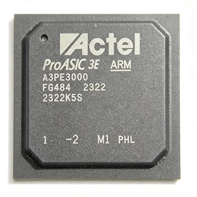
A3PE3000-1FGG484 - 3M-Gate ProASIC3E Flash FPGA | Microchip
MPN: A3PE3000-1FGG484 ✓ نشط| الكمية | سعر الوحدة | الإجمالي |
|---|---|---|
| 1 | $1782.14 | $1,782.14 |
| 10 | $1693.03 | $16,930.30 |
| 100 | $1603.93 | $160,393.00 |
| 500 | $1514.82 | $757,410.00 |
| 1,000 | $1425.71 | $1,425,710.00 |
A3PE3000-1FGG484 نظرة عامة
A flash FPGA is a field-programmable gate array whose configuration is stored in on-chip non-volatile flash memory rather than an external configuration device. Within the programmable logic hierarchy, the ProASIC3E family sits above smaller ProASIC3 parts and is positioned as a single-chip, low-total-cost-of-ownership solution: because the bitstream is stored on-chip, no external flash boot device is required, and the FPGA is inherently secure against bitstream interception.
Key features of the A3PE3000-1FGG484 include instant-on power-up (the fabric is active within microseconds of power application), reprogrammability without a microprocessor, low dynamic power from the 1.5V core, and an abundance of advanced features typical of the ProASIC3E family, including embedded memory blocks and support for the Cortex-M1 soft processor in related M1 ProASIC3 variants. The 341 available user I/O support multiple single-ended and differential standards for flexible board-level integration.
Architecturally, the device uses Microchip (formerly Actel/Microsemi) 130nm flash technology with a fine-grained fabric of versatile logic elements, routing resources, and distributed embedded flash memory totaling 516,096 bits. The 484-ball FBGA with 1 mm pitch balances I/O density with solderability on standard PCB assembly lines.
Typical applications include industrial automation and motor control, aerospace and defense systems requiring non-volatile, secure configuration, medical instrumentation, and communications equipment where single-chip instant-on logic replaces CPLD-plus-FPGA two-chip solutions.
When designing with this device, confirm the industrial temperature variant (A3PE3000-1FGG484I) if the end environment exceeds commercial ranges, and budget power distribution for the 1.5V core rail. Pricing on distributor channels is roughly $1,782 per unit for the industrial variant as of 2026-09-02.
This page synthesizes distributor pricing, same-footprint drop-in alternatives across the ProASIC3E and ProASIC3L families, and practical design notes not found in the manufacturer datasheet.
بدائل مباشرة لـ A3PE3000-1FGG484 — نفس الحزمة، متوافق دبوس بدبوس. تُستثنى القطع ذات الحزم المختلفة التي تتطلب تعديل PCB.
الطرازات في هذه السلسلة
طرازات من نفس السلسلة متوافقة تمامًا مع A3PE3000-1FGG484 (نفس عامل الشكل والبصمة) — يختلف في Package, Family, Process Technology, RoHS Status, Operating Temperature.
أداة المقارنة السريعة — اختر قطعًا بديلة للمقارنة جنبًا إلى جنب:
A3PE3000-1FGG484I
✅ بديل مباشرتواصل لمعرفة السعر
عرض ورقة البيانات ←A3PE3000-FGG484
✅ بديل مباشرتواصل لمعرفة السعر
عرض ورقة البيانات ←A3PE3000-FGG484I
✅ بديل مباشر✗ غير متوفر
$1451.56 / وحدة
عرض ورقة البيانات ←A3PE3000-2FGG484I
✅ بديل مباشرتواصل لمعرفة السعر
عرض ورقة البيانات ←A3PE3000L-1FGG484
✅ بديل مباشرتواصل لمعرفة السعر
عرض ورقة البيانات ←A3PE3000L-FGG484I
✅ بديل مباشرتواصل لمعرفة السعر
عرض ورقة البيانات ←A3PE3000-1FGG484 الحدود القصوى والخصائص الكهربائية
| Family | ProASIC3E |
| System Gates | 3,000,000 |
| Logic Cells | 75264 |
| User I/O | 341 |
| Embedded Memory Bits | 516096 |
| Maximum System Frequency | 231 MHz |
| Process Technology | 130 nm flash |
| Core Supply Voltage | 1.5 V |
| Speed Grade | -1 |
| العلبة | 484-ball FBGA (FGG484) |
| Package Dimensions | 23 x 23 mm |
| Ball Pitch | 1 mm |
| Package Height | 2.23 mm |
| نوع التركيب | Surface Mount |
| Configuration Memory | On-chip flash (non-volatile, single-chip) |
| حالة RoHS | Compliant (lead-free per Kynix listing) |
دليل تكوين أطراف A3PE3000-1FGG484 2.23 mm
تكوين الأطراف لـ A3PE3000-1FGG484 (حزمة 2.23 mm). تتضمن هذه الدائرة المتكاملة الرقمية GPIO وواجهات الاتصال (UART وSPI وI2C) وأطراف الطاقة. راجع ورقة بيانات الشركة المصنعة لوظائف الأطراف البديلة وخيارات التكوين. ضرورية لتصميم الأنظمة المدمجة وتخطيط PCB.

لا تتوفر بيانات مفصلة لمخطط التوصيلات لـ A3PE3000-1FGG484.
راجع ورقة البيانات للحصول على تكوين الأطراف الكامل.
التطبيقات النموذجية
A3PE3000-1FGG484 مناسب لـ 6 التطبيقs: Industrial Automation and Motor Control, Aerospace and Defense Systems, Medical Instrumentation, Communications and Networking Equipment, Secure Single-Chip Embedded Systems, Test and Measurement Instrumentation.
Industrial Automation and Motor Control
The A3PE3000-1FGG484 fits industrial control backplanes and multi-axis motor controllers where deterministic instant-on logic is required at power-up. Its 75,264 logic cells and 341 user I/O provide enough capacity to integrate PWM generation, encoder interfaces, and safety interlock logic in a single chip, while 516,096 bits of embedded memory buffer telemetry and recipe data. Because configuration is stored on-chip in flash, production lines start immediately without a boot sequence, and the 1.5V core keeps dynamic power acceptable in sealed cabinets. Place the FPGA between 24V field-side isolation and the backplane interface, using its I/O banks for 3.3V/2.5V standards; the 231 MHz-class fabric comfortably closes timing on 100 MHz-class control loops.
موصى به
Aerospace and Defense Systems
ProASIC3E flash FPGAs are a mainstay in avionics, satellites, and defense electronics because the configuration bitstream resides in secure on-chip flash with no external configuration device to read, intercept, or fail. The A3PE3000-1FGG484 supplies 3 million system gates and 341 I/O for payload data formatting, bus bridging, and telemetry aggregation, with instant-on behavior valuable in power-cycled flight scenarios. The 484-ball 23 x 23 mm FBGA supports reliable solder attachment on high-reliability assembly lines. For programs with wide temperature requirements, the pin-compatible A3PE3000-1FGG484I industrial variant is the standard substitution; verify screening requirements against program specifications before final selection.
موصى به
Medical Instrumentation
Medical imaging front-ends, patient monitors, and diagnostic analyzers benefit from the A3PE3000-1FGG484's single-chip, non-volatile architecture: no configuration PROM means one fewer component to qualify and a reduced failure surface in long-lifecycle instruments. The 75,264 logic elements implement sensor timing controllers, filter accelerators, and interface bridges, while 341 I/O banks connect ADCs, displays, and communication modules at 3.3V/2.5V/1.8V standards. The 1.5V core reduces dynamic power, simplifying thermal design in fanless bedside equipment. Designers should allocate I/O banks so analog-adjacent signals use the quietest banks and follow Microchip's layout guidance for the 1 mm-pitch FBGA escape routing.
موصى به
Communications and Networking Equipment
In line cards, aggregation switches, and wireless infrastructure, the A3PE3000-1FGG484 serves as glueless bridge logic between MACs, PHYs, and backplanes, using its 341 I/O to span multiple voltage domains. The 516,096-bit embedded memory implements FIFOs and descriptor rings, and the 231 MHz-class fabric closes timing for 125-156 MHz interface clocks common in MII/GMII-adjacent designs. Because the fabric is active within microseconds of power application, link supervision and safety shut-off logic operate before software boots, an advantage over SRAM FPGAs that wait for configuration. Estimated: dynamic power scales with toggle rate - use SmartPower analysis when budgeting the 1.5V core rail.
موصى به
Secure Single-Chip Embedded Systems
Applications that must resist cloning and bitstream theft - payment terminals, license-control hardware, cryptographic accelerators - choose the A3PE3000-1FGG484 because flash-based configuration cannot be read out like SRAM configuration bits, and no external boot flash exists to dump. The 3M-gate fabric hosts AES-class logic and system controllers, and 516,096 bits of embedded memory stores keys and counters. Instant-on operation means security logic enforces policy from the first microsecond of power. The 484-ball FBGA (23 x 23 mm, 1 mm pitch) suits both cost-sensitive and high-reliability assembly; pair with Microchip secure memory or authentication ICs for device-identity architectures.
موصى به
Test and Measurement Instrumentation
Bench instruments, protocol analyzers, and automated test equipment use the A3PE3000-1FGG484 as a flexible timing, trigger, and interface engine. Its 341 I/O connect to probe front ends, pattern generators, and host interfaces across multiple I/O standards, while the 231 MHz-class fabric and 75,264 logic elements implement deep trigger state machines and timestamping with the 516,096-bit embedded memory as capture buffers. Non-volatile configuration lets instruments pass calibration self-test immediately at power-up, and field firmware updates are applied through JTAG using Microchip Libero tooling. The industrial -1FGG484I variant suits portable instruments exposed to wide ambient ranges in the identical 484-ball footprint.
موصى به
ملخص المنتجات الموصى بها
بيانات مرجعية هندسية لـ A3PE3000-1FGG484 — المقارنة وإرشادات التصميم ومعلومات الامتثال.
دليل الاختيار
المقارنة مع البدائل
| المعامل | هذا المنتج | A3PE3000-1FGG484I | A3PE3000-FGG484 | A3PE3000-2FGG484I | A3PE3000L-1FGG484 |
|---|---|---|---|---|---|
| Package | 484-ball FBGA (FGG484), 23 x 23 mm | 484-ball FBGA (FGG484) - same | 484-ball FBGA (FGG484) - same | 484-ball FBGA (FGG484) - same | 484-ball FBGA (FGG484) - same |
| Brand | Microchip Technology | Microchip Technology | Microchip Technology | Microchip Technology | Microchip Technology |
| System Gates | 3,000,000 | 3,000,000 | 3,000,000 | 3,000,000 | 3,000,000 |
| Speed Grade | -1 | -1 | Standard (slower) | -2 (faster) | -1 class |
| User I/O | 341 | 341 | 341 | 341 | 341 |
| Core Supply Voltage | 1.5 V | 1.5 V | 1.5 V | 1.5 V | 1.5 V |
| Temperature Range | Commercial | Industrial (-40C to +100C class) | Commercial | Industrial (-40C to +100C class) | Commercial |
| Power Profile | Standard ProASIC3E dynamic power | Same as this product | Lower (slower speed grade) | Higher (faster speed grade) | Lower (ProASIC3L low-power process) |
أبرز الفروقات
- Faster -1 speed grade at identical footprint (مقابلA3PE3000-FGG484)
- Industrial temperature option without redesign (مقابلA3PE3000-1FGG484I)
- Lower power alternative in the same package (مقابلA3PE3000L-1FGG484)
- Single-chip non-volatile configuration (مقابلXC6SLX9 (Xilinx Spartan-6, cross-brand))
ملاحظات التصميم
The A3PE3000-1FGG484 requires a regulated 1.5V core supply plus per-bank VCCI rails for the I/O standards in use. Estimated: dynamic core current scales with clock frequency and logic toggle rate - run Microchip SmartPower in Libero SoC with your post-place-and-route design to size the core regulator before committing hardware. Decouple each VCCI bank with local ceramic capacitors (10uF bulk plus 0.1uF per bank) placed within a few millimeters of the associated balls. Sequence supplies so external drivers do not back-power I/O banks before their rails stabilize.
Escape routing for the 484-ball, 1 mm-pitch FBGA (23 x 23 mm) typically requires via-in-pad or dog-bone escapes with 4-mil trace/space on at least a 4-layer board; dedicate internal layers to a solid ground plane under the package for return-current integrity. Solder the package with a standard lead-free reflow profile compatible with RoHS SAC305 balls, and inspect with X-ray given the 1 mm pitch. Do not route high-speed signals on the outer layer directly beneath the die area without an adjacent reference plane.
Order the correct temperature suffix: the commercial A3PE3000-1FGG484 and industrial A3PE3000-1FGG484I share the same footprint and pinout, so a commercial part specified into an industrial build will not be caught by layout review. Also confirm speed grade in the Libero constraint file matches the purchased device (-1 here); a mismatch causes timing closure to be optimistic. Finally, remember that unlike SRAM FPGAs, no external configuration flash is needed - do not copy boot-flash circuitry from Spartan-6 reference designs.
With 341 user I/O across multiple banks, assign simultaneous-switching groups carefully: distribute high-toggle-count buses across banks and VCCI domains to reduce ground bounce on the shared return path. The 1 mm ball pitch introduces stub inductance; for the fastest single-ended standards, use Microchip's IBIS models from the product page in your board-level simulations. Differential pairs should be length-matched from ball to receiver, keeping the escape region symmetrical to avoid skew introduced by via stubs.
معلومات الامتثال
Kynix listing marks A3PE3000-1FGG484 as LEAD FREE; Xecor database records RoHS Code Yes for the FGG484 package (23 x 23 mm, green package description). REACH and halogen-free declarations not found in provided data.
