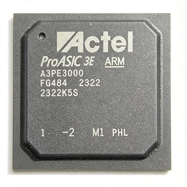
A3PE3000-1FGG484 - 3M-Gate ProASIC3E Flash FPGA | Microchip
부품 번호: A3PE3000-1FGG484 ✓ 활성| 수량 | 단가 | 합계 |
|---|---|---|
| 1 | $1782.14 | $1,782.14 |
| 10 | $1693.03 | $16,930.30 |
| 100 | $1603.93 | $160,393.00 |
| 500 | $1514.82 | $757,410.00 |
| 1,000 | $1425.71 | $1,425,710.00 |
A3PE3000-1FGG484 개요
A flash FPGA is a field-programmable gate array whose configuration is stored in on-chip non-volatile flash memory rather than an external configuration device. Within the programmable logic hierarchy, the ProASIC3E family sits above smaller ProASIC3 parts and is positioned as a single-chip, low-total-cost-of-ownership solution: because the bitstream is stored on-chip, no external flash boot device is required, and the FPGA is inherently secure against bitstream interception.
Key features of the A3PE3000-1FGG484 include instant-on power-up (the fabric is active within microseconds of power application), reprogrammability without a microprocessor, low dynamic power from the 1.5V core, and an abundance of advanced features typical of the ProASIC3E family, including embedded memory blocks and support for the Cortex-M1 soft processor in related M1 ProASIC3 variants. The 341 available user I/O support multiple single-ended and differential standards for flexible board-level integration.
Architecturally, the device uses Microchip (formerly Actel/Microsemi) 130nm flash technology with a fine-grained fabric of versatile logic elements, routing resources, and distributed embedded flash memory totaling 516,096 bits. The 484-ball FBGA with 1 mm pitch balances I/O density with solderability on standard PCB assembly lines.
Typical applications include industrial automation and motor control, aerospace and defense systems requiring non-volatile, secure configuration, medical instrumentation, and communications equipment where single-chip instant-on logic replaces CPLD-plus-FPGA two-chip solutions.
When designing with this device, confirm the industrial temperature variant (A3PE3000-1FGG484I) if the end environment exceeds commercial ranges, and budget power distribution for the 1.5V core rail. Pricing on distributor channels is roughly $1,782 per unit for the industrial variant as of 2026-09-02.
This page synthesizes distributor pricing, same-footprint drop-in alternatives across the ProASIC3E and ProASIC3L families, and practical design notes not found in the manufacturer datasheet.
드롭인 대체품: A3PE3000-1FGG484 — 동일 패키지, 핀 호환. PCB 재작업이 필요한 다른 패키지 부품은 제외됩니다.
이 시리즈의 변형
다음과 드롭인 호환되는 동일 시리즈 모델: A3PE3000-1FGG484 (동일 폼 팩터 및 풋프린트) — 차이점: Package, Family, Process Technology, RoHS Status, Operating Temperature.
빠른 비교 도구 — 나란히 비교할 대체 부품을 선택하십시오:
A3PE3000-1FGG484I
✅ 드롭인✓ 재고 있음
$1336.6 / 개
데이터시트 보기 →A3PE3000-FGG484
✅ 드롭인✓ 재고 있음
$152.6 / 개
데이터시트 보기 →A3PE3000-FGG484I
✅ 드롭인✓ 재고 있음
$1451.56 / 개
데이터시트 보기 →A3PE3000-2FGG484I
✅ 드롭인✓ 재고 있음
$89.4 / 개
데이터시트 보기 →A3PE3000L-1FGG484
✅ 드롭인✓ 재고 있음
$134 / 개
데이터시트 보기 →A3PE3000L-FGG484I
✅ 드롭인✓ 재고 있음
가격 문의
데이터시트 보기 →A3PE3000-1FGG484 최대 정격 & 전기적 특성
| Family | ProASIC3E |
| System Gates | 3,000,000 |
| Logic Cells | 75264 |
| User I/O | 341 |
| Embedded Memory Bits | 516096 |
| Maximum System Frequency | 231 MHz |
| Process Technology | 130 nm flash |
| Core Supply Voltage | 1.5 V |
| Speed Grade | -1 |
| 패키지 | 484-ball FBGA (FGG484) |
| Package Dimensions | 23 x 23 mm |
| Ball Pitch | 1 mm |
| Package Height | 2.23 mm |
| 실장 유형 | Surface Mount |
| Configuration Memory | On-chip flash (non-volatile, single-chip) |
| RoHS 상태 | Compliant (lead-free per Kynix listing) |
A3PE3000-1FGG484 2.23 mm 핀 구성 가이드
A3PE3000-1FGG484(2.23 mm 패키지)의 핀 구성입니다. 이 디지털 IC에는 GPIO, 통신 인터페이스(UART, SPI, I2C), 전원 핀이 포함되어 있습니다. 대체 핀 기능과 구성 옵션은 제조사 데이터시트를 참조하십시오. 임베디드 시스템 설계와 PCB 레이아웃에 필수적입니다.

다음에 대한 상세 핀아웃 데이터 없음: A3PE3000-1FGG484.
다음을 참조하십시오: 데이터시트 전체 핀 구성은 다음을 참조하십시오.
일반적인 애플리케이션
A3PE3000-1FGG484 적합 용도: 6 애플리케이션s: Industrial Automation and Motor Control, Aerospace and Defense Systems, Medical Instrumentation, Communications and Networking Equipment, Secure Single-Chip Embedded Systems, Test and Measurement Instrumentation.
Industrial Automation and Motor Control
The A3PE3000-1FGG484 fits industrial control backplanes and multi-axis motor controllers where deterministic instant-on logic is required at power-up. Its 75,264 logic cells and 341 user I/O provide enough capacity to integrate PWM generation, encoder interfaces, and safety interlock logic in a single chip, while 516,096 bits of embedded memory buffer telemetry and recipe data. Because configuration is stored on-chip in flash, production lines start immediately without a boot sequence, and the 1.5V core keeps dynamic power acceptable in sealed cabinets. Place the FPGA between 24V field-side isolation and the backplane interface, using its I/O banks for 3.3V/2.5V standards; the 231 MHz-class fabric comfortably closes timing on 100 MHz-class control loops.
추천
Aerospace and Defense Systems
ProASIC3E flash FPGAs are a mainstay in avionics, satellites, and defense electronics because the configuration bitstream resides in secure on-chip flash with no external configuration device to read, intercept, or fail. The A3PE3000-1FGG484 supplies 3 million system gates and 341 I/O for payload data formatting, bus bridging, and telemetry aggregation, with instant-on behavior valuable in power-cycled flight scenarios. The 484-ball 23 x 23 mm FBGA supports reliable solder attachment on high-reliability assembly lines. For programs with wide temperature requirements, the pin-compatible A3PE3000-1FGG484I industrial variant is the standard substitution; verify screening requirements against program specifications before final selection.
추천
Medical Instrumentation
Medical imaging front-ends, patient monitors, and diagnostic analyzers benefit from the A3PE3000-1FGG484's single-chip, non-volatile architecture: no configuration PROM means one fewer component to qualify and a reduced failure surface in long-lifecycle instruments. The 75,264 logic elements implement sensor timing controllers, filter accelerators, and interface bridges, while 341 I/O banks connect ADCs, displays, and communication modules at 3.3V/2.5V/1.8V standards. The 1.5V core reduces dynamic power, simplifying thermal design in fanless bedside equipment. Designers should allocate I/O banks so analog-adjacent signals use the quietest banks and follow Microchip's layout guidance for the 1 mm-pitch FBGA escape routing.
추천
Communications and Networking Equipment
In line cards, aggregation switches, and wireless infrastructure, the A3PE3000-1FGG484 serves as glueless bridge logic between MACs, PHYs, and backplanes, using its 341 I/O to span multiple voltage domains. The 516,096-bit embedded memory implements FIFOs and descriptor rings, and the 231 MHz-class fabric closes timing for 125-156 MHz interface clocks common in MII/GMII-adjacent designs. Because the fabric is active within microseconds of power application, link supervision and safety shut-off logic operate before software boots, an advantage over SRAM FPGAs that wait for configuration. Estimated: dynamic power scales with toggle rate - use SmartPower analysis when budgeting the 1.5V core rail.
추천
Secure Single-Chip Embedded Systems
Applications that must resist cloning and bitstream theft - payment terminals, license-control hardware, cryptographic accelerators - choose the A3PE3000-1FGG484 because flash-based configuration cannot be read out like SRAM configuration bits, and no external boot flash exists to dump. The 3M-gate fabric hosts AES-class logic and system controllers, and 516,096 bits of embedded memory stores keys and counters. Instant-on operation means security logic enforces policy from the first microsecond of power. The 484-ball FBGA (23 x 23 mm, 1 mm pitch) suits both cost-sensitive and high-reliability assembly; pair with Microchip secure memory or authentication ICs for device-identity architectures.
추천
Test and Measurement Instrumentation
Bench instruments, protocol analyzers, and automated test equipment use the A3PE3000-1FGG484 as a flexible timing, trigger, and interface engine. Its 341 I/O connect to probe front ends, pattern generators, and host interfaces across multiple I/O standards, while the 231 MHz-class fabric and 75,264 logic elements implement deep trigger state machines and timestamping with the 516,096-bit embedded memory as capture buffers. Non-volatile configuration lets instruments pass calibration self-test immediately at power-up, and field firmware updates are applied through JTAG using Microchip Libero tooling. The industrial -1FGG484I variant suits portable instruments exposed to wide ambient ranges in the identical 484-ball footprint.
추천
추천 제품 요약
엔지니어링 참조 데이터: A3PE3000-1FGG484 — 비교, 설계 지침 및 규정 준수 정보.
선택 가이드
대체품과의 비교
| 파라미터 | 이 제품 | A3PE3000-1FGG484I | A3PE3000-FGG484 | A3PE3000-2FGG484I | A3PE3000L-1FGG484 |
|---|---|---|---|---|---|
| Package | 484-ball FBGA (FGG484), 23 x 23 mm | 484-ball FBGA (FGG484) - same | 484-ball FBGA (FGG484) - same | 484-ball FBGA (FGG484) - same | 484-ball FBGA (FGG484) - same |
| Brand | Microchip Technology | Microchip Technology | Microchip Technology | Microchip Technology | Microchip Technology |
| System Gates | 3,000,000 | 3,000,000 | 3,000,000 | 3,000,000 | 3,000,000 |
| Speed Grade | -1 | -1 | Standard (slower) | -2 (faster) | -1 class |
| User I/O | 341 | 341 | 341 | 341 | 341 |
| Core Supply Voltage | 1.5 V | 1.5 V | 1.5 V | 1.5 V | 1.5 V |
| Temperature Range | Commercial | Industrial (-40C to +100C class) | Commercial | Industrial (-40C to +100C class) | Commercial |
| Power Profile | Standard ProASIC3E dynamic power | Same as this product | Lower (slower speed grade) | Higher (faster speed grade) | Lower (ProASIC3L low-power process) |
주요 차별점
- Faster -1 speed grade at identical footprint (vs A3PE3000-FGG484)
- Industrial temperature option without redesign (vs A3PE3000-1FGG484I)
- Lower power alternative in the same package (vs A3PE3000L-1FGG484)
- Single-chip non-volatile configuration (vs XC6SLX9 (Xilinx Spartan-6, cross-brand))
설계 노트
The A3PE3000-1FGG484 requires a regulated 1.5V core supply plus per-bank VCCI rails for the I/O standards in use. Estimated: dynamic core current scales with clock frequency and logic toggle rate - run Microchip SmartPower in Libero SoC with your post-place-and-route design to size the core regulator before committing hardware. Decouple each VCCI bank with local ceramic capacitors (10uF bulk plus 0.1uF per bank) placed within a few millimeters of the associated balls. Sequence supplies so external drivers do not back-power I/O banks before their rails stabilize.
Escape routing for the 484-ball, 1 mm-pitch FBGA (23 x 23 mm) typically requires via-in-pad or dog-bone escapes with 4-mil trace/space on at least a 4-layer board; dedicate internal layers to a solid ground plane under the package for return-current integrity. Solder the package with a standard lead-free reflow profile compatible with RoHS SAC305 balls, and inspect with X-ray given the 1 mm pitch. Do not route high-speed signals on the outer layer directly beneath the die area without an adjacent reference plane.
Order the correct temperature suffix: the commercial A3PE3000-1FGG484 and industrial A3PE3000-1FGG484I share the same footprint and pinout, so a commercial part specified into an industrial build will not be caught by layout review. Also confirm speed grade in the Libero constraint file matches the purchased device (-1 here); a mismatch causes timing closure to be optimistic. Finally, remember that unlike SRAM FPGAs, no external configuration flash is needed - do not copy boot-flash circuitry from Spartan-6 reference designs.
With 341 user I/O across multiple banks, assign simultaneous-switching groups carefully: distribute high-toggle-count buses across banks and VCCI domains to reduce ground bounce on the shared return path. The 1 mm ball pitch introduces stub inductance; for the fastest single-ended standards, use Microchip's IBIS models from the product page in your board-level simulations. Differential pairs should be length-matched from ball to receiver, keeping the escape region symmetrical to avoid skew introduced by via stubs.
규정 준수 정보
Kynix listing marks A3PE3000-1FGG484 as LEAD FREE; Xecor database records RoHS Code Yes for the FGG484 package (23 x 23 mm, green package description). REACH and halogen-free declarations not found in provided data.
