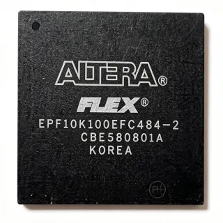
LFE2-20E-5F484C - 21K LUT FPGA, 331 I/O | Lattice
MPN: LFE2-20E-5F484C ✗ انتهى عمره الإنتاجيLFE2-20E-5F484C نظرة عامة
An FPGA is a programmable semiconductor whose lookup tables, registers, interconnect, and dedicated blocks can be configured after manufacture. The LFE2-20E-5F484C belongs to the ECP2 FPGA family and provides a hardware platform for parallel logic, state machines, interfaces, control logic, and DSP pipelines. Its 331 I/O make the package especially useful when the design requires substantial external connectivity.
The supplied distributor information identifies the device as an ECP2 FPGA with 21K LUTs, 331 I/O, DSP support, 1.2 V operation, and a -5 speed designation. The package is identified as 484-BBGA. Detailed timing, memory, configuration, electrical, and temperature data are not present in the supplied source excerpts, so those values are not asserted here. The design should be checked against the manufacturer datasheet before layout, power budgeting, or production qualification.
A -5 FPGA speed designation indicates the manufacturer’s speed-grade family, but the operating-temperature grade and timing margins are not stated in the verified excerpts. The 1.2 V core supply is the confirmed supply value, while external I/O supply requirements, configuration voltage, and power consumption require the full manufacturer documentation. The 484-BBGA package requires a PCB footprint and thermal design appropriate for a large fine-pitch BGA.
Typical design uses include industrial automation, communications equipment, video and image processing, embedded control, and general-purpose programmable logic. The large I/O count can support external memory, parallel buses, sensor interfaces, transceiver connections, and control peripherals. DSP capability can reduce external processing hardware when the design uses fixed-point or parallel signal-processing functions implemented within the FPGA.
For a new PCB, preserve the exact Lattice package pinout and ball assignment, define clean power and ground planes, and validate high-speed routing with the complete timing and pinout documentation. Do not treat distributor snippets as a substitute for the manufacturer datasheet. This page consolidates the verified distributor identity, package, density, I/O, voltage, and sourcing information while explicitly separating unknown technical details.
The practical advantage of this part is its combination of moderate FPGA logic density, extensive I/O, DSP support, and a 1.2 V core architecture. It is more suitable than a small logic device when a design needs substantial parallel connectivity, while the -5 grade should be selected only after confirming timing requirements against the complete Lattice documentation.
بدائل مباشرة لـ LFE2-20E-5F484C — نفس الحزمة، متوافق دبوس بدبوس. تُستثنى القطع ذات الحزم المختلفة التي تتطلب تعديل PCB.
الطرازات في هذه السلسلة
طرازات من نفس السلسلة متوافقة تمامًا مع LFE2-20E-5F484C (نفس عامل الشكل والبصمة) — يختلف في Package, Package Type, Speed Grade, DSP Capability, Terminal Count.
LFE2-20E-5F484I
✅ بديل مباشرتواصل لمعرفة السعر
عرض ورقة البيانات ←LFE2-20E-5FN484C
✅ بديل مباشر📋 بديل مرجعي (غير موجود في الكتالوج)
LFEC20E-5F484C
✅ بديل مباشر📋 بديل مرجعي (غير موجود في الكتالوج)
LFE2M20SE-5F484C
✅ بديل مباشر📋 بديل مرجعي (غير موجود في الكتالوج)
LFE2-20E-5F484C
✅ بديل مباشرتواصل لمعرفة السعر
عرض ورقة البيانات ←LFE2-20E-5F484C الحدود القصوى والخصائص الكهربائية
| Device Type | ECP2 Field Programmable Gate Array (FPGA) |
| Logic Cell Density | 21K LUTs |
| Input/Output Count | 331 I/O |
| Core Supply Voltage | 1.2 V |
| Speed Grade | -5 |
| DSP Capability | DSP |
| العلبة | 484-BBGA |
| Package Type | BGA |
| Terminal Count | 484 balls |
| نوع التركيب | Surface Mount |
| Programmable Device | Yes |
| FPGA Family | LatticeECP2 |
| Logic Technology | 90 nm CMOS |
دليل تكوين أطراف LFE2-20E-5F484C bga
تكوين الأطراف لـ LFE2-20E-5F484C (حزمة bga). تتضمن هذه الدائرة المتكاملة الرقمية GPIO وواجهات الاتصال (UART وSPI وI2C) وأطراف الطاقة. راجع ورقة بيانات الشركة المصنعة لوظائف الأطراف البديلة وخيارات التكوين. ضرورية لتصميم الأنظمة المدمجة وتخطيط PCB.

لا تتوفر بيانات مفصلة لمخطط التوصيلات لـ LFE2-20E-5F484C.
راجع ورقة البيانات للحصول على تكوين الأطراف الكامل.
التطبيقات النموذجية
LFE2-20E-5F484C مناسب لـ 6 التطبيقs: Industrial Automation Control, Communications and Network Interface, Video and Image Processing, Embedded Control and Data Acquisition, DSP Accelerator and Signal Processing, Test and Measurement Equipment.
Industrial Automation Control
LFE2-20E-5F484C fits industrial automation designs that combine parallel control logic with numerous external fieldbus, sensor, actuator, and machine-interface signals. Its verified 21K LUT capacity provides substantial programmable logic for sequencing, state machines, interlocks, and diagnostics, while 331 I/O can reduce the need for external interface expansion. The 484-BBGA package also provides a high pin count for routed control buses and dedicated peripheral connections. Before release, verify timing margins, I/O standards, power rails, and the exact pin map in the Lattice documentation.
موصى به
Communications and Network Interface
The ECP2 FPGA architecture of LFE2-20E-5F484C is suitable for communications equipment requiring parallel packet handling, fixed-function protocol logic, and flexible I/O allocation. The 21K LUT figure supports moderate protocol processing and control functions, while the 331 I/O count can accommodate data buses, control signals, and multiple external interfaces. The -5 speed designation should be validated against the required clock rate using the complete family timing data. Confirm the FPGA’s supported I/O standards, configuration method, and signal-integrity requirements before layout.
موصى به
Video and Image Processing
LFE2-20E-5F484C can serve as a programmable front end for image and video systems that require parallel pixel, timing, control, and data-processing logic. Its 21K LUTs and DSP capability are useful for deterministic filtering, feature extraction, color processing, or test-pattern generation, while 331 I/O provides connectivity to sensors, memory, serializers, and display controllers. The exact supported I/O voltage, memory interface, and maximum video timing must be verified in the manufacturer datasheet. The 484-BBGA footprint requires careful ball-escape and signal-integrity planning.
موصى به
Embedded Control and Data Acquisition
The LFE2-20E-5F484C is appropriate for embedded control systems that require deterministic hardware logic alongside sensor acquisition and actuator control. A design can use LUTs and registers for timing, filtering, sequencing, and protocol handling, while DSP blocks can accelerate fixed-point arithmetic. The 331 I/O figure allows direct connection to multiple sensors, switches, memories, and converters, reducing external glue logic when pin resources are carefully assigned. Verify electrical limits, configuration storage, clocking, and power sequencing in the full manufacturer documentation.
موصى به
DSP Accelerator and Signal Processing
The verified DSP capability of LFE2-20E-5F484C makes it useful for fixed-point filtering, waveform generation, correlation, and parallel signal-processing pipelines. The 21K LUT capacity allows surrounding control, addressing, and data-format logic to be integrated with the DSP blocks, reducing the need for separate programmable logic in suitable designs. Performance depends on the exact DSP architecture, clocking, memory resources, and speed grade, which are not supplied in the excerpts. Confirm those details and the I/O budget before committing to the device.
موصى به
Test and Measurement Equipment
LFE2-20E-5F484C can support programmable test and measurement systems that coordinate sequencing, acquisition, pattern generation, and result analysis. Its 331 I/O can connect test fixtures, status signals, clocks, memories, and communication ports, while 21K LUTs support timing and control logic around the DSP resources. The large 484-BBGA package demands careful thermal, power, and escape-routing design. Timing margins, I/O standards, and any high-speed interface requirements must be validated with the complete Lattice documentation before production.
موصى به
ملخص المنتجات الموصى بها
بيانات مرجعية هندسية لـ LFE2-20E-5F484C — المقارنة وإرشادات التصميم ومعلومات الامتثال.
دليل الاختيار
المقارنة مع البدائل
| المعامل | هذا المنتج | LFE2-20E-5F484I | LFE2-20E-5FN484C | LFEC20E-5F484C | LFE2M20SE-5F484C | LFE2-20E-5F484C |
|---|---|---|---|---|---|---|
| Package | 484-BBGA | 484-BBGA family candidate | 484-BBGA | 484-BBGA family candidate | 484-BBGA family candidate | 484-BBGA |
| Brand | Lattice Semiconductor | Lattice Semiconductor | Lattice Semiconductor | Lattice Semiconductor | Lattice Semiconductor | Lattice Semiconductor |
أبرز الفروقات
- High verified I/O availability for parallel systems (مقابلLFE2-20E-5F484I)
- DSP capability is explicitly identified for the target (مقابلLFEC20E-5F484C)
- Confirmed core supply and speed designation (مقابلLFE2M20SE-5F484C)
ملاحظات التصميم
Start the layout by obtaining the manufacturer’s exact 484-BBGA ball map, land pattern, and escape-routing guidance. Reserve continuous power and ground planes, place decoupling close to the relevant supply balls, and route high-speed signals with controlled impedance. Because the verified data confirms the package and ball count but not the full pinout or stack-up requirements, do not finalize the PCB footprint from distributor summaries alone.
Build the power tree around the verified 1.2 V core requirement, then confirm every auxiliary and I/O supply from the complete Lattice datasheet. Separate noisy digital activity from sensitive analog or external interface sections where practical, and validate power sequencing against configuration requirements. The supplied excerpts do not state current consumption, tolerance, startup behavior, or decoupling values, so those values must not be guessed.
A 484-BBGA design requires disciplined escape routing and signal-integrity planning. Keep clock and configuration paths short, avoid routing high-speed signals through power-plane splits, and use the manufacturer’s recommended ball assignments and I/O standards. Establish a timing-closure plan around the -5 speed designation and the actual clock targets. The verified excerpts do not provide maximum frequency or I/O timing values, so validation must use the complete family documentation.
Do not substitute a related Lattice MPN solely because it has a similar 484-BBGA package. Confirm logic resources, I/O count, voltage rails, speed grade, temperature grade, configuration method, memory resources, and qualification. The cross-reference results name several candidates, but search snippets are not proof of drop-in equivalence. Verify the exact ordering table and pin map before releasing a replacement or respin.
معلومات الامتثال
The supplied verified data does not state RoHS, REACH, lead-free, halogen-free, conflict-mineral, or automotive qualification status for LFE2-20E-5F484C. AEC-Q100 is recorded as not applicable because the verified data does not identify this device as an automotive-qualified part.