What Is the A3PE3000-FGG484I and Why Does It Matter for Your Design?
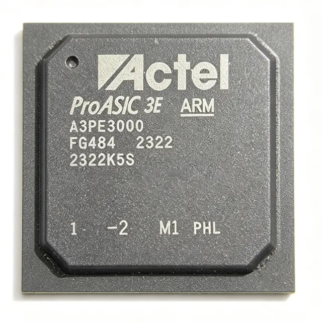
The Microchip Technology (Microsemi) A3PE3000-FGG484I is a ProASIC3E flash-based FPGA delivering 3 million system gates (75,264 logic cells), 341 user I/Os, and 516,096 bits of embedded RAM in a 484-ball Fine-Pitch Ball Grid Array (FBGA) package measuring 23 x 23 mm with a 1 mm ball pitch. It operates from a single 1.5V core on 130nm flash-based CMOS technology and is rated for the industrial temperature range of -40C to +100C. Because configuration lives in on-chip nonvolatile flash cells, the device is live at power-up with no external boot PROM or configuration flash — a single-chip solution that lowers BOM cost, saves board space, and improves configuration security versus SRAM FPGAs that must reload a bitstream at every power cycle.
Availability is strong on XAIPART: the part is lifecycle-active with deep stock on hand (over 99,999 units listed), MOQ of 1, and tiered pricing starting at $1,782.14 at quantity 1, stepping down to $1,451.56 at quantity 1,000, as of 2026-09-02. The ProASIC3E family is distinguished from SRAM FPGAs by its nonvolatile flash configuration cells, which eliminates bitstream interception risk at the configuration-storage level and supports systems with fast-start requirements. Typical applications include industrial automation and motor control, aerospace and defense subsystems, medical instrumentation, communications bridging, and test equipment — precisely the environments where nonvolatile, secure, instant-on programmable logic is required.
Quick Answers — What Do Buyers and Engineers Most Need to Know?
Buyers evaluating the A3PE3000-FGG484I most frequently ask about price, stock, substitutes, and whether the part still fits new designs. The verified facts: it is an industrial-grade (-40C to +100C) 484-ball FBGA ProASIC3E part, priced from $1,782.14 (qty 1) to $1,451.56 (qty 1,000) as of 2026-09-02 on XAIPART, lifecycle status active, and supported by Microchip's Libero SoC design suite. Same-footprint drop-in replacements within the Microchip ProASIC3 family include A3PE3000-2FGG484I (faster '-2' speed grade), A3PE3000-FG484I, and the low-power A3PE3000L-FGG484I / A3PE3000L-1FGG484I variants — all pin-compatible in the 484-BGA footprint. There is no true cross-brand drop-in equivalent: Lattice MachXO2, Xilinx Spartan-6 XC6SLX9, and Intel MAX 10 are only functional alternatives requiring PCB rework and design recompilation. Two database gaps to close before BOM approval: RoHS status and moisture sensitivity level (MSL) are not confirmed in our records — see the verification notes on this page and validate against the official Microchip datasheet.
How Do You Select and Design In the A3PE3000-FGG484I?
Confirm the Package, Temperature Grade, and Speed Grade First
The FGG484 package is a 484-ball FBGA, 23 x 23 mm, 1 mm pitch, surface-mount with ball terminals. The trailing 'I' suffix is critical: it denotes the industrial grade (-40C to +100C), while the non-suffixed A3PE3000-FGG484 is the commercial grade (0C to +85C). Both share the identical die, 3M gates, 341 I/Os, and 484-ball FGG484 package, so they are pin-compatible drop-ins — but only the -I part is qualified for industrial temperature environments. Speed grades matter too: the standard-grade FGG484I is the baseline, and the A3PE3000-2FGG484I carries the faster '-2' speed grade in the same pinout. Validate I/O switching characteristics at your target interface rates against the '-1', standard, or '-2' speed grade selection before finalizing the BOM.
Plan the Power Architecture Around the 1.5V Core
The A3PE3000-FGG484I operates from a single 1.5V core on 130nm flash technology. I/O bank voltages support multiple standards across the 341 user I/Os; verify I/O bank voltages against the datasheet for mixed-voltage sensor or backplane interfaces. For low-power designs, note the trade-off: the standard A3PE3000 draws higher static power than the A3PE3000L low-power variant, which uses a lower core voltage. Budget thermal margins accordingly in convection-cooled or enclosed systems, or evaluate the A3PE3000L-FGG484I in the same footprint where the power budget allows.
Leverage the Flash Fabric at the Board Level
Because configuration is stored in on-chip flash, no configuration controller or boot device consumes board space. This shortens system boot: the flash fabric is live at power-up, so safety interlock logic and backplane handshaking are active within microseconds of power application, versus SRAM FPGAs that spend milliseconds reloading bitstreams. In-system reprogrammability supports field firmware updates without hardware changes or boot-device swaps. For high-pin-count interfaces — wide memory buses, many peripherals — the full 341 user I/Os of the FGG484I are the deciding factor; the A3PE3000-PQ208I exposes far fewer I/O pins and suits only I/O-light designs, with identical 3M-gate logic density.
Pin Assignment and Design Flow
The complete 484-ball pinout is published in the ProASIC3E family datasheet's package/pinout tables on the Microchip product page. Given 484 ball positions, reproduce the map only from the official document: use the Microchip datasheet package chapter together with Libero SoC's I/O constraint editor for bank-accurate pin assignments. Avoid third-party datasheet mirror sites, as their revisions may be outdated relative to Microchip's current release.
Export Control and Compliance Checks
The ECCN classification is 3A001.A.2.C, which applies to export control. Procurement teams on aerospace and defense programs should validate licensing requirements early in the program rather than at production release. REACH compliance is listed as compliant per parametric records for the A3PE3000 family; RoHS status and MSL are unconfirmed in our database and must be verified against the official Microchip datasheet before finalizing BOM approvals.
What Are the Drop-in Alternatives and How Do They Compare?
Only same-family Microchip/Microsemi ProASIC3 parts in the 484-ball FGG484 package are pin-compatible drop-ins. Verified substitutes from our records: A3PE3000-2FGG484I (faster '-2' speed grade, similar substitute per FindIC classification with consistent functional characteristics but different electrical/timing characteristics), A3PE3000-FG484I, and the ProASIC3L low-power variants A3PE3000L-FGG484I and A3PE3000L-1FGG484I (same package, same 3M-gate density and 341 I/Os, lower core voltage and reduced static power — verify timing closure and power supply sequencing with your Libero design before swapping). The table below shows the verified spec set for the A3PE3000-FGG484I; detailed electrical parameters for the substitutes are not in our database and must come from their own datasheets.
| Parameter | A3PE3000-FGG484I |
|---|---|
| Family | ProASIC3E |
| System Gates | 3,000,000 |
| Logic Cells | 75,264 |
| User I/O | 341 |
| Embedded RAM Bits | 516,096 |
| Core Voltage | 1.5 V |
| Technology | 130 nm flash-based CMOS |
| Package | 484-ball FBGA (FGG484), 23 x 23 mm, 1 mm pitch |
| Operating Temperature | -40C to +100C (Industrial) |
| Configuration Memory | Nonvolatile Flash (live at power-up) |
| Terminal Count / Form | 484 / Ball |
| Mounting Type | Surface Mount |
| ECCN | 3A001.A.2.C |
| REACH Compliance | Compliant (per parametric records for A3PE3000 family) |
| RoHS Status | [DATA_NEEDED: RoHS status of A3PE3000-FGG484I] |
| Moisture Sensitivity Level | [DATA_NEEDED: MSL level] |
Cross-brand note: Web comparisons suggest Lattice MachXO2, Xilinx Spartan-6 XC6SLX9, and Intel MAX 10 as functional alternatives of broadly similar class, but these use different packages, pinouts, voltage rails, and toolchains (Libero vs Diamond/ISE/Quartus). A functional replacement requires PCB rework and design recompile — no cross-brand FPGA substitutes on the existing 484-BGA footprint.
What Is the Market Position, Lifecycle Status, and Supply Situation of the A3PE3000-FGG484I?
The A3PE3000-FGG484I is listed with an active part life-cycle code in parametric databases as of 2026-09-02, and Microchip maintains the ProASIC3E family including Libero SoC design suite support. Supply signals on XAIPART are strong: over 99,999 units in stock with MOQ 1, and tiered pricing from $1,782.14 (qty 1) down to $1,451.56 (qty 1,000) as of 2026-09-02. Octopart tracks availability across 7 distributors as of 2026-09-02, and the FAQ records note that high-density ProASIC3E parts frequently show long lead times — mature Microsemi/Microchip ProASIC3E parts often carry multi-week to multi-month factory lead times when distributor stock is exhausted. Check the availability indicator on the product page before committing a build. Lead time is not fixed and depends on distributor stock position. [DATA_NEEDED: unit shipment and market share data for the ProASIC3E family — not provided in verified data.]
What Trends Should Buyers Watch for This Component?
First, watch speed-grade strategy: because A3PE3000-2FGG484I is a pin-compatible drop-in with faster timing, dual-sourcing your BOM across the standard and '-2' grades protects schedules when interface-rate timing budgets tighten. Second, watch the power trade-off: the ProASIC3L low-power variants (A3PE3000L-FGG484I, A3PE3000L-1FGG484I) offer the same footprint and density with reduced core power, making them the natural second source for battery or convection-cooled designs — but verify timing closure and power-supply sequencing in Libero before swapping. Third, watch configuration security requirements: the on-chip flash configuration of the A3PE3000-FGG484I eliminates the externally readable boot device that SRAM FPGA designs require, and live-at-power-up behavior removes boot-time windows — a growing procurement criterion in secure embedded control. Fourth, manage the maturity risk: this is a 130nm product family, so for new designs evaluate stock depth and factory lead times proactively, and quote multiple distributors in parallel. Finally, close the compliance gaps: RoHS status and MSL remain unconfirmed in our database, and the 3A001.A.2.C ECCN requires export-license validation on controlled programs.
Comments
Be the first to comment.
🔐 Please sign in to post a comment.
Don't have an account? Sign up