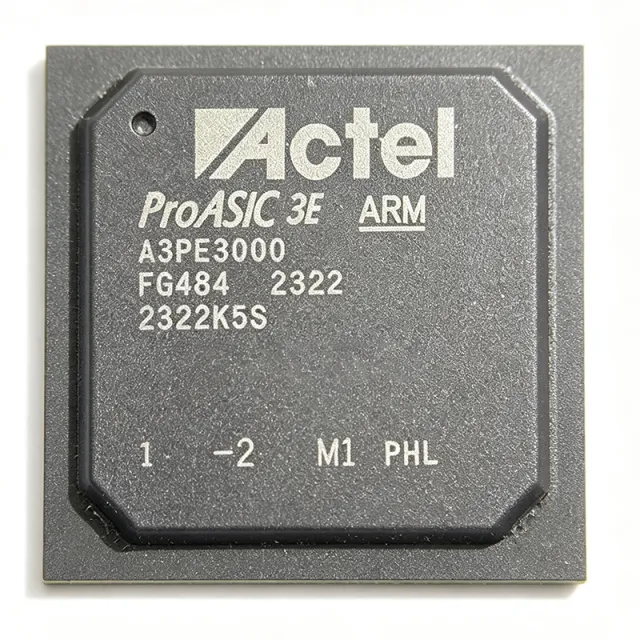
A3PE3000-FGG484I - ProASIC3E FPGA 3M Gates 484-FBGA | Microchip
MPN: A3PE3000-FGG484I ✓ Active| Qty | Unit Price | Extended |
|---|---|---|
| 1 | $1782.14 | $1,782.14 |
| 10 | $1693.03 | $16,930.30 |
| 100 | $1608.38 | $160,838.00 |
| 500 | $1527.96 | $763,980.00 |
| 1,000 | $1451.56 | $1,451,560.00 |
A3PE3000-FGG484I Overview
A field-programmable gate array (FPGA) is a semiconductor device containing a fabric of programmable logic blocks and interconnects that designers configure in the field. The ProASIC3E family sits in the flash-based FPGA hierarchy: FPGA -> programmable logic device -> programmable SoC/system logic, distinguished from SRAM FPGAs by its nonvolatile flash configuration cells.
Key features include flash-based live-at-power-up operation with no external configuration device, single 1.5V core operation on 130nm flash technology, low total cost of ownership through single-chip integration, and reprogrammability without a boot PROM. The 341 I/Os support multiple standards, and the 23x23 mm FBGA footprint suits high-IO industrial designs.
Architecturally, the A3PE3000 uses a sea-of-vanilla logic tile fabric with Versatile routing, flash switch blocks, and embedded SRAM blocks totalling 516,096 bits. Because configuration is stored in flash, the device is inherently secure against bitstream interception and instantly active at power-up - critical for systems with fast-start requirements.
Typical applications include industrial automation and motor control, aerospace and defense subsystems, medical instrumentation, communications bridging, and test equipment where nonvolatile, secure, instant-on programmable logic is required.
A key design consideration: the FGG484I is the industrial-grade, RoHS-code-No variant in some parametric databases, so verify environmental compliance requirements against the official Microchip datasheet before finalizing BOM approvals.
This page synthesizes distributor pricing signals, drop-in same-footprint alternatives, and practical design notes not found on the manufacturer product page alone.
Drop-in alternatives for A3PE3000-FGG484I — same package, pin-to-pin compatible. Different-package parts requiring PCB rework are excluded.
Variants in this series
Same-series models that are drop-in compatible with A3PE3000-FGG484I (same form factor and footprint) — differing in Package, Family, Configuration Memory, Process Technology, RoHS Status.
Quick Comparison Tool — Select alternative parts for side-by-side comparison:
A3PE3000-2FGG484I
✓ In Stock
$89.4 / Unit
View Datasheet →A3PE3000-1FGG484I
✓ In Stock
$1336.6 / Unit
View Datasheet →A3PE3000-FG484I
✓ In Stock
$98.6 / Unit
View Datasheet →A3PE3000L-FGG484I
✓ In Stock
Contact for price
View Datasheet →A3PE3000L-1FGG484I
✓ In Stock
$104.5 / Unit
View Datasheet →A3PE3000L-FG484I
✓ In Stock
Contact for price
View Datasheet →A3PE3000-FGG484I Maximum Ratings & Electrical Characteristics
| Family | ProASIC3E |
| System Gates | 3000000 |
| Logic Cells | 75264 |
| User I/O | 341 |
| Embedded RAM Bits | 516096 |
| Core Voltage | 1.5 V |
| Technology | 130 nm flash-based CMOS |
| Package | 484-ball FBGA (FGG484), 23 x 23 mm, 1 mm pitch |
| Operating Temperature | -40C to +100C (Industrial) |
| Configuration Memory | Nonvolatile Flash (live at power-up) |
| Mounting Type | Surface Mount |
| Terminal Form | Ball |
| Terminal Count | 484 |
| REACH Compliance | Compliant (per parametric records for A3PE3000 family) |
| ECCN | 3A001.A.2.C |
A3PE3000-FGG484I 484-ball fbga (fgg484), 23 x 23 mm, 1 mm pitch Pin Configuration Guide
Pin configuration for A3PE3000-FGG484I (484-ball fbga (fgg484), 23 x 23 mm, 1 mm pitch package). This digital IC includes GPIO, communication interfaces (UART, SPI, I2C), and power pins. Refer to the manufacturer datasheet for alternate pin functions and configuration options. Essential for embedded system design and PCB layout.

No detailed pinout data available for A3PE3000-FGG484I.
Refer to the datasheet for full pin configuration.
Typical Applications
A3PE3000-FGG484I is suitable for 6 applications: Industrial Automation and Motor Control, Aerospace and Defense Subsystems, Medical Instrumentation, Communications Bridging and Line Cards, Test and Measurement Equipment, Secure Embedded Control Systems.
Industrial Automation and Motor Control
The A3PE3000-FGG484I fits industrial automation because its -40C to +100C industrial rating and 3M-gate flash fabric handle PLC, drive, and motion-control logic without external configuration memory. The 341 user I/Os let one device interface encoder inputs, PWM outputs, and multiple fieldbus transceivers simultaneously, while 516,096 bits of embedded RAM buffer control tables and communication frames. Because the flash fabric is live at power-up, safety interlock logic is active within microseconds of power application - a quantified advantage over SRAM FPGAs that spend milliseconds reloading bitstreams. Place it between a main MCU and high-pin-count I/O conditioning circuits; the trade-off is higher static power than the low-power A3PE3000L variant, so budget thermal margins accordingly.
Recommended
Aerospace and Defense Subsystems
Aerospace and defense designs value the A3PE3000-FGG484I for its nonvolatile flash configuration, which eliminates the external bitstream storage that SRAM FPGAs require and reduces attack surface for configuration tampering. The 3M-gate capacity accommodates glue logic consolidation, bus bridging (MIL-STD-class interfaces implemented in fabric), and payload data formatting, while 341 I/Os support wide parallel interfaces in a single 23x23 mm package. Single 1.5V core operation simplifies power supply design in size- and weight-constrained avionics boxes. The ECCN classification 3A001.A.2.C applies to export control, so procurement teams should validate licensing requirements early in the program rather than at production release.
Recommended
Medical Instrumentation
Medical diagnostic and monitoring equipment benefits from the A3PE3000-FGG484I's instant-on flash fabric for patient-safety interlocks and deterministic acquisition sequencing. The 3M-gate density implements multichannel signal-conditioning state machines, trigger logic, and interface bridging between analog front ends and host processors, with 516,096 bits of embedded SRAM used for capture FIFOs. The 484-ball FGG484 footprint provides 341 I/Os, enough to connect numerous sensor channels and control lines without external fan-out logic, reducing board count in portable and cart-based instruments. Verify I/O bank voltages against the datasheet for mixed-voltage sensor interfaces, and consider the A3PE3000L variant when battery operation or reduced heat in an enclosed enclosure is a requirement.
Recommended
Communications Bridging and Line Cards
In communications equipment, the A3PE3000-FGG484I serves as a protocol and backplane bridge: its 341 I/Os and 3M gates handle parallel-to-serial adaptation, framing, and multi-standard I/O termination across card interfaces. The embedded 516,096-bit SRAM implements elastic buffers and descriptor FIFOs between asynchronous clock domains, a common requirement in line-card designs. Because the flash fabric is live at power-up, backplane handshaking is available immediately, and no configuration controller consumes board space on dense cards. The single-chip flash solution also simplifies field firmware logistics - reprogramming happens in-system without swapping boot devices. Designers should validate I/O switching characteristics at their target interface rates against the '-1', standard, or '-2' speed grade selection.
Recommended
Test and Measurement Equipment
Bench and automated test instruments use the A3PE3000-FGG484I as timing, trigger, and channel-control fabric. The 3M-gate capacity implements per-channel pattern generators and comparators, while 341 I/Os drive dense connector interfaces directly - important where channel counts determine instrument value. Embedded SRAM supports deep capture buffers between the analog/digital front end and a host CPU, and the deterministic, instant-on flash configuration guarantees repeatable instrument startup sequences required in calibration-sensitive measurements. The industrial temperature range suits both laboratory and field-deployed testers. When the timing budget is tight, choose the '-2' speed grade drop-in; when the tester is battery or convection-cooled, evaluate the A3PE3000L low-power variant in the same footprint.
Recommended
Secure Embedded Control Systems
Embedded controllers that must resist configuration cloning or bitstream interception choose the A3PE3000-FGG484I because configuration lives in on-chip flash cells rather than an externally readable flash device. The 3M-gate fabric consolidates microcontroller peripherals, custom accelerators, and interface glue into one 484-ball device, cutting BOM count and simplifying supply-chain security audits. Live-at-power-up behavior removes boot-time windows that attackers or fault monitors could exploit, and in-system reprogrammability supports field firmware updates without hardware changes. The industrial -40C to +100C rating covers unconditioned enclosures. Trade-off: flash FPGAs of this generation are 130nm, so for compute-heavy workloads a modern SRAM FPGA may offer more raw performance at the cost of configuration-security complexity.
Recommended
Recommended Products Summary
Engineering reference data for A3PE3000-FGG484I — comparison, design guidance, and compliance information.
Selection Guide
Comparison with Alternatives
| Parameter | This Product | A3PE3000-2FGG484I | A3PE3000-1FGG484I | A3PE3000L-FGG484I | A3PE3000L-1FGG484I |
|---|---|---|---|---|---|
| Package | 484-ball FBGA (FGG484) | 484-ball FBGA (FGG484) - same | 484-ball FBGA (FGG484) - same | 484-ball FBGA (FGG484) - same | 484-ball FBGA (FGG484) - same |
| Brand | Microchip Technology | Microchip Technology | Microchip Technology | Microchip Technology | Microchip Technology |
| System Gates | 3,000,000 | 3,000,000 | 3,000,000 | 3,000,000 | 3,000,000 |
| User I/O | 341 | 341 | 341 | 341 | 341 |
| Speed Grade | Standard | -2 (faster) | -1 (slower) | Standard (L family) | -1 (slower, L family) |
| Family / Power | ProASIC3E (standard power) | ProASIC3E (standard power) | ProASIC3E (standard power) | ProASIC3L (low power) | ProASIC3L (low power) |
| Operating Temperature | -40C to +100C (Industrial) | -40C to +100C (Industrial) | -40C to +100C (Industrial) | -40C to +100C (Industrial) | -40C to +100C (Industrial) |
Key Differentiators
- Standard speed grade at lower cost than fast grade (vs A3PE3000-2FGG484I)
- Full industrial temperature qualification (vs A3PE3000-FGG484)
- Standard power fabric for maximum timing headroom (vs A3PE3000L-FGG484I)
Design Notes
The A3PE3000-FGG484I operates from a 1.5V core on the ProASIC3E fabric. Estimate total power using Microchip's Libero SoC SmartPower tool with your post-place-and-route netlist rather than worst-case datasheet numbers - static and dynamic power depend heavily on utilization, toggle rates, and I/O standards. Because the standard ProASIC3E draws more static power than the ProASIC3L low-power variant, verify that your supply and thermal budget accommodate the difference if you migrate between the two same-footprint parts.
The FGG484 is a 1 mm-pitch, 23x23 mm FBGA requiring controlled-impedance fan-out; plan at least one inner layer for the ball breakout fan vias. Decouple each VCC/VCCIO bank with a network of 0.1 uF ceramics placed within 2-3 mm of the bank balls, plus bulk capacitance per supply domain. Follow Microchip's ProASIC3E user I/O bank guide to keep bank voltage domains consistent before committing the ball assignment, since changing bank assignments after layout is costly.
Common pitfalls when substituting within the A3PE3000 family: (1) the '-1', standard, and '-2' speed grades share the package footprint but not timing - re-run static timing analysis in Libero SoC after any speed-grade swap; (2) migrating to the A3PE3000L changes core power characteristics and requires power-rail re-verification even though the footprint is identical; (3) the FGG484I is industrial grade while non-suffixed parts are commercial - do not substitute in -40C designs. Always confirm RoHS/finish requirements (FG vs FGG) against current Microchip documents.
Compliance Information
Parametric records for the A3PE3000 family list REACH compliant and ECCN 3A001.A.2.C; RoHS code conflicts across sources (some records show 'No' for FGG484I, 'Yes' for related variants) - verify against the official Microchip product page before BOM approval.







