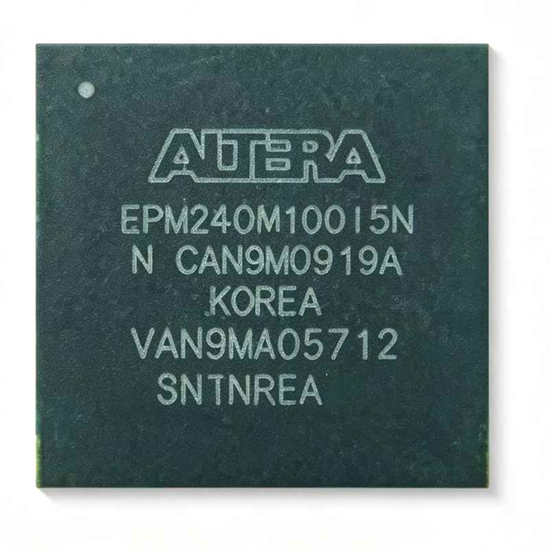
Quick Answers: What Is the EPM240GM100I5N and Is It Available?
The Intel EPM240GM100I5N is a non-volatile MAX II complex programmable logic device (CPLD) with 240 logic elements, 192 equivalent macrocells, 80 user I/O pins, and a 4.7 ns pin-to-pin propagation delay (tPD1). It ships in a 100-ball Micro FineLine BGA (MBGA) measuring 6 mm x 6 mm with 0.5 mm ball pitch, runs from a 1.8 V core supply (VCCINT), and supports MultiVolt I/O banks at 1.5 V, 1.8 V, 2.5 V, 3.3 V, or 5 V across an industrial -40 C to +105 C range. Availability is strong: the part is in active production with 99,999 units in XAIPART stock at MOQ 1, priced from $68.1818 (qty 1) down to $39.7727 (qty 1,000) as of 2026-09-16.
Flash-based configuration makes the device instant-on. It comes out of power-on reset fully configured within microseconds and needs no external configuration PROM and no boot loader. An embedded 8-Kbit User Flash Memory (UFM) block stores serial numbers, calibration constants, or boot parameters that user logic reads at startup. In-system programming runs over JTAG (IEEE 1149.1) from Intel Quartus Prime or legacy Quartus II with a USB-Blaster or Byte-Blaster download cable.
The table below consolidates the verified specification set for this ordering code.
| Parameter | Verified value |
|---|---|
| Family | MAX II |
| Logic elements | 240 |
| Equivalent macrocells | 192 |
| User I/O pins | 80 |
| User Flash Memory (UFM) | 8 Kbits |
| Pin-to-pin delay (tPD1) | 4.7 ns |
| Maximum internal operating frequency | 300 MHz |
| Process technology | 0.18 um 6-layer-metal flash CMOS |
| Configuration memory | On-chip non-volatile flash (instant-on) |
| Core supply (VCCINT) | 1.8 V |
| MultiVolt I/O (VCCIO) | 1.5 V / 1.8 V / 2.5 V / 3.3 V / 5 V |
| Package | 100-ball Micro FineLine BGA, 6 mm x 6 mm, 0.5 mm pitch |
| Operating temperature | -40 C to +105 C (industrial) |
| Mounting type | Surface mount |
| RoHS / lead-free | Lead-free per package marking |
| Programming interface | JTAG (IEEE 1149.1) ISP |
| Lifecycle status | Active |
| XAIPART stock / MOQ | 99,999 units / 1 |
| XAIPART pricing (as of 2026-09-16) | $68.1818 @ 1; $49.2424 @ 10; $43.5606 @ 100; $41.6667 @ 500; $39.7727 @ 1,000 |
That combination of 36 mm2 of board area, 80 user I/O pins, and mixed 1.8 V to 5 V interfacing on a single die is what lets the part replace discrete 74-series glue logic, older MAX 7000-series CPLDs that required external boot memory, and small gate arrays. The MAX II family itself spans 240 to 2,210 logic elements on the same 0.18 um flash process, so designs that outgrow 240 LEs can move up within the family without changing the configuration methodology.
Supply looks healthy today. XAIPART holds 99,999 units at MOQ 1, the XAIPART database lists the device as active (not NRND and not obsolete), and authorized distributors including DigiKey (part number EPM240GM100I5N-ND) and Mouser Electronics list MBGA-100 inventory in cut-tape and full-reel quantities as of 2026-09-12. Factory-direct lead time for production reels is approximately 8-12 weeks. You can check current tier pricing and quantity breaks on the EPM240GM100I5N product page.
How Do You Select and Design In the EPM240GM100I5N?
Start with the power architecture
The device needs one 1.8 V core rail (VCCINT) and up to four independent VCCIO bank rails. In the MBGA-100 pin-out, VCCINT is sourced from balls C4, C6, F4, F7, J5, and J7; VCCIO1 from B2 and B8; VCCIO2 from D3, D8, and E5; VCCIO3 from E6 and H4; and VCCIO4 from H5, H7, K2, and K8. Each bank can be powered independently at 1.5 V, 1.8 V, 2.5 V, 3.3 V, or 5 V, so a single 6 mm x 6 mm CPLD can bridge a 5 V legacy microcontroller bus and a 1.8 V application processor without external level shifters.
Decoupling must include at least one 0.1 uF X7R ceramic capacitor per VCC pin, placed as close as possible to the package balls. That guidance matters more here than on a large TQFP because the fine 0.5 mm ball pitch limits the space available for via fan-out on the inner power balls. Build the decoupling plan before you finalize the ball map, not after.
Plan the JTAG and configuration interface
JTAG pin assignments are fixed on this device: TMS on F5, TCK on F6, TDI on G4, TDO on G6. The nCONFIG ball (G5) is a configuration control input with a pull-up, and nSTATUS (G7) is a configuration status output with a pull-up. Route a standard four-signal JTAG header plus power and ground, and keep the JTAG chain separate from high-speed I/O to avoid injected noise on TCK.
Because the configuration bitstream lives in on-chip non-volatile flash, no external configuration PROM is required and zero boot latency is introduced. Design work is done in Intel Quartus Prime or the legacy Altera Quartus II toolchain, which handles synthesis, place-and-route, timing analysis, JTAG programming, and generation of the in-system programmability file. Quartus Prime Lite edition supports the MAX II family at no cost, which keeps non-recurring engineering cost low for small-volume and educational builds - a real advantage over FPGA architectures that need external boot devices plus a larger package.
Commit to the MBGA-100 footprint early
The 100-ball MBGA occupies 36 mm2, with 80 balls dedicated to user I/O and the remaining 20 assigned to power, ground, JTAG, and configuration. The package eliminates the lead-footprint concerns of larger TQFP packages, but it does require PCB-level fine-pitch assembly capability at 0.5 mm ball pitch. Frame the land pattern and stencil aperture design before layout freeze; changing between MBGA-100 and FBGA-100 later forces a full board redesign.
Signal integrity deserves explicit attention. Validate high-speed outputs above 100 MHz on the bench, because the small ball pitch can introduce crosstalk onto adjacent traces. Keep high-slew outputs away from sensitive analog or clock nets, and use ground-referenced stripline routing where the I/O count allows it.
Close timing with real numbers
The 4.7 ns pin-to-pin delay (tPD1) and 300 MHz maximum internal operating frequency are the two figures that drive most selection decisions. For address latching, chip-select generation, and bus arbitration, the 4.7 ns tPD1 comfortably handles 50-100 MHz bus speeds, including the 155 MHz side-band signaling used on telecom line cards. Use the Quartus timing analyzer output rather than the headline tPD1 alone, because fan-out and routing choices extend worst-case delay in a real design. After any device substitution, re-run timing closure to confirm setup and hold margins.
Use the UFM for identity and constants
The 8-Kbit UFM block is the feature that separates this part from simple glue logic. Store line-card serial numbers and manufacturing traceability data, timing calibration constants the decoder references at startup, or boot configuration words for a host processor. Memory content is accessible over the JTAG chain, which means field service can read board identity without powering the full system into application mode.
Match the device to the application
The application profile that fits best is I/O expansion and bus bridging between a low-pin-count microcontroller and external SRAM, NOR flash, or parallel-port peripherals, where 80 MultiVolt I/O pins absorb address latching, chip-select, and bus-arbitration duties. Power-up and power-down sequencing for multi-rail FPGA and SoC boards is a second strong fit: the CPLD boots instantly and its 80 I/O pins drive enable signals, power-good inputs, and reset lines in parallel. Industrial control glue logic in PLCs and motor controllers benefits from the -40 C to +105 C rating and the JTAG in-system programming path that allows field firmware updates without pulling a module from service. Telecom line-card framing and alarm aggregation, plus display and set-top-box control tasks such as EDID access, HDMI hot-plug-detect logic, and front-panel key-scan matrices, round out the verified application set.
Worked example: a power-up sequencing controller
A multi-rail board with an FPGA, DDR memory, and a legacy 5 V peripheral bus needs deterministic sequencing. Configure the EPM240GM100I5N as the sequencing controller: assign a 3.3 V VCCIO bank to the power-good inputs and a second bank to the enable outputs, then implement sequence delays and fault monitoring in the logic fabric. The 4.7 ns tPD1 is negligible against millisecond-scale rail rise times, so sequence accuracy is set by the counter clock, not by the CPLD. With a 300 MHz maximum internal frequency, the internal clock period is 3.33 ns, giving fine-grained timer resolution if a fast watchdog re-trigger path is required. The 80 user I/O pins support dozens of enable, power-good, and reset signals without I/O expansion. Explore the wider device set in the FPGA and CPLD category.
What Are the Drop-In Alternatives to the EPM240GM100I5N?
The alternatives that matter are the same-die variants inside the MAX II family. The EPM240GM100C5N uses the identical MBGA-100 footprint and the same MAX II G 192-macrocell die, differing only in temperature grade. The EPM240M100I5N is pin-compatible in the 100-pin Micro FineLine BGA with identical pin-outs and timing specifications; the G variant adds a separate VCCIO bank configuration that can further reduce power in mixed-voltage designs, so the difference is a power profile rather than a logic change. The EPM240F100I5N and EPM240GF100I5N are electrically similar but use the FBGA-100 ball map, which makes them non-drop-in on an MBGA-100 land pattern.
| Parameter | EPM240GM100I5N | EPM240GM100C5N | EPM240M100I5N | EPM240F100I5N |
|---|---|---|---|---|
| Manufacturer / family | Intel, MAX II G | Intel, MAX II G | Intel, MAX II (non-G) | Intel, MAX II G |
| Die / logic capacity | 240 LEs, 192 macrocells | Same MAX II G 192-macrocell die | Pin-compatible with identical pin-outs and timing specifications | Same MAX II G 192-macrocell die |
| Package | 100-ball Micro FineLine BGA, 6 mm x 6 mm, 0.5 mm pitch | Identical MBGA-100 footprint | 100-pin Micro FineLine BGA (pin-compatible) | FBGA-100 (different ball map) |
| Operating temperature | -40 C to +105 C (industrial, I5) | 0 C to +85 C (commercial, C5) | Industrial I5 suffix | Industrial I5 suffix |
| Pin-to-pin delay (tPD1) | 4.7 ns | Same tPD1 timing bin as the I5N | Identical timing specifications to the I5N | Electrically similar per verified FAQ data |
| VCCIO / MultiVolt behavior | Four banks at 1.5 V / 1.8 V / 2.5 V / 3.3 V / 5 V | MultiVolt I/O on the same die | Non-G variant; G adds separate VCCIO bank configuration for lower power in mixed-voltage designs | MultiVolt I/O on the same die |
| Drop-in status | Reference part | Drop-in footprint, commercial temperature only | Pin-compatible drop-in, marginally different power profile | Not a drop-in - board re-layout required |
Cross-brand substitution is a different matter. Lattice and Xilinx do not produce a pin-compatible replacement for this part in the MBGA-100 footprint with the same 192-macrocell count. Lattice ispMACH 4000ZE devices and Xilinx CoolRunner-II devices use different ball maps, different JTAG IDs, and different design toolchains, so switching to them requires a board redesign plus full re-implementation of the HDL source. They are functional equivalents, not drop-in parts. The XAIPART verified alternatives dataset for this ordering code contains no additional pin-compatible cross-brand entries beyond the MAX II family parts described above.
Whichever path you take, re-run Quartus timing closure after substitution to confirm hold and setup margins, and re-check the JTAG chain order if the replacement part sits in the middle of a scan chain. For more background on choosing between programmable logic classes, see the MAX II CPLD design guide.
Where Does the EPM240GM100I5N Stand in the Market and Supply Chain?
Lifecycle status in the XAIPART database is active. The part is not listed as NRND and not listed as obsolete, and it remains in volume production. XAIPART holds 99,999 units with an MOQ of 1, so prototyping and production pulls can be filled from the same inventory position.
Verified tier pricing as of 2026-09-16 runs $68.1818 at quantity 1, $49.2424 at 10, $43.5606 at 100, $41.6667 at 500, and $39.7727 at 1,000. The 1,000-piece price is about 41.7 percent below the single-unit price, a spread worth planning purchase orders around.
On the distribution side, DigiKey (part number EPM240GM100I5N-ND) and Mouser Electronics carry MBGA-100 inventory in cut-tape and full-reel quantities as of 2026-09-12, and Octopart aggregates live multi-distributor pricing and on-order quantities. Factory-direct lead time for production reels is approximately 8-12 weeks as of 2026-09-12. For high-volume programs of 10,000 units or more, a scheduled volume agreement through an Intel or Altera field applications engineer is the standard route to lock pricing and lead time.
Competitively, the MAX II series targets the lowest-power, lowest-cost segment of the programmable logic market. It displaces discrete 74-series glue logic and small gate arrays, and its 0.18 um process with a 1.8 V core delivers lower dynamic and standby current than earlier MAX 7000-series CPLDs that also required external boot memory. Two caveats are worth stating plainly. First, the verified dataset used for this article does not include units-shipped or market-share figures for the MAX II family, so third-party market-size claims should be validated independently. Second, automotive-grade AEC-Q100 qualification is not claimed on the MAX II family, so this part is intended for industrial, consumer, and communications applications rather than automotive safety systems.
What Should Buyers Watch in the CPLD Market?
Watch the price ladder, not the list price. With a verified spread of $68.1818 at quantity 1 versus $39.7727 at quantity 1,000 as of 2026-09-16, consolidating demand into fewer, larger releases is the single highest-leverage cost action on this part. Buffer inventory is cheap relative to the tier step between 10 and 100 pieces.
Match the temperature grade to the environment, not to habit. The I5N suffix designates the industrial -40 C to +105 C grade. The C5N variant shares the same MBGA-100 footprint and the same MAX II G 192-macrocell die but is rated for the commercial 0 C to +85 C range. Don't over-specify the industrial grade for indoor equipment, but don't shop on price assumptions either - the verified pricing in this dataset covers the I5N part only. Outdoor telecom, factory automation, and digital-signage kiosks are the cases that justify industrial grade.
Lock the footprint before layout freeze. The MBGA-100 land pattern (6 mm x 6 mm, 0.5 mm pitch) and the FBGA-100 land pattern are not interchangeable despite sharing the die and logic capacity. Selection between the GM100 and F100 ordering codes is purely a PCB-footprint decision, and getting it wrong is a re-layout, not a re-order.
Plan VCCIO banks with the modern interface in mind. MultiVolt I/O at 1.5 V through 5 V is the reason this device survives in designs that mix legacy 5 V peripherals with 1.8 V processors. Note that the G variant adds separate VCCIO bank configuration that can further reduce power in mixed-voltage designs - relevant if the board has strict thermal or power budgets, such as a NEBS-constrained telecom line card.
Budget bench time for signal integrity above 100 MHz. The 0.5 mm ball pitch is the trade-off for the 36 mm2 footprint. Crosstalk validation on adjacent traces is not optional at high toggle rates, and it is cheaper to fix in layout than in EMC testing.
Keep the toolchain and the alternate part in the AVL. Quartus Prime Lite supports the MAX II family at no cost, so there is no licensing barrier to keeping a second source programmed and tested. Because the device is flash-configured with no external boot PROM, a pin-compatible alternate can be validated with a single JTAG re-program rather than a board change. Monitor Intel product change notices against the current datasheet revision to catch packaging or marking changes early, and treat the 8-Kbit UFM as part of the migration plan - serial numbers and calibration constants must be re-programmed whenever the device is swapped.
Comments
Be the first to comment.
🔐 Please sign in to post a comment.
Don't have an account? Sign up