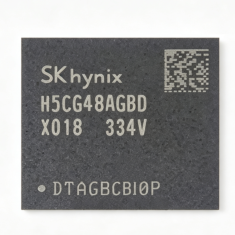
The SK hynix H5CG48AGBDX018N is a 16Gb DDR5 SDRAM memory IC organized as 2Gx8 with an 8-bit data bus, operating at data rates up to 5600 Mbps from a 1.1V nominal supply in an 82-ball FCBGA (JEDEC DDR5 78/82-ball) surface-mount package rated for -40C to +85C operation. The part belongs to SK hynix's A-die generation of DDR5 and is currently active in the lifecycle with strong availability: XAIPART lists 99,999 units in stock with MOQ 1, priced at $87.42 per unit as of 2026-09-12, and aggregate distributor availability exceeded 50,000 pieces as of early September 2026. Typical applications include server main memory, AI and high-performance computing modules, industrial controllers, embedded logging memory, and consumer computing platforms. This guide consolidates verified specifications, design-in guidance, validated drop-in alternatives, and sourcing strategy for this constrained DDR5 line item.
Quick Answers: What Is the H5CG48AGBDX018N?
The H5CG48AGBDX018N is SK hynix's 16Gb (2G x 8) DDR5 SDRAM in the A-die generation, delivering DDR5-5600 signaling on a JEDEC DDR5 interface with a 1.1V core supply. Like all DDR5 devices, it supports on-die ECC, decision-feedback equalization (DFE) on the DQ receivers, and an I3C-based sideband bus for host control — generation-standard features that sustain signal integrity at 5600 Mbps on conventional PCB stackups. The x8 organization simplifies memory controller configuration and ECC implementation in both module and solder-down designs.
Compared with DDR4, DDR5 doubles the bank count, moves the power management IC (PMIC) onto the memory module, reduces the per-channel word length to 16 bits, and lowers the operating voltage from 1.2V to 1.1V — raising bandwidth while improving power efficiency. The H5CG48AGBDX018N's -40C to +85C rating per distributor data extends its use beyond consumer computing into industrial environments.
Key verified specifications at a glance:
| Parameter | Value |
|---|---|
| Memory Type | DDR5 SDRAM |
| Density | 16 Gb (2G x 8) |
| Organization | 2G x 8 |
| Data Rate | 5600 Mbps |
| Supply Voltage | 1.1 V |
| Bus Width | 8 bit |
| Package | 82-ball FCBGA (JEDEC DDR5 78/82-ball) |
| Mounting Type | Surface Mount |
| Operating Temperature | -40C to +85C |
| Interface | JEDEC DDR5 |
| Memory Generation | DDR5 (SK hynix A-die) |
| Price / Stock | $87.42, 99,999 units, MOQ 1 (as of 2026-09-12) |
Technical Guide: How Do You Design In the H5CG48AGBDX018N?
Power Delivery: Why the 1.1V Rail Matters
DDR5 moves the power management function from the host board onto memory modules. When you solder the H5CG48AGBDX018N die directly to a custom PCB (a non-DIMM design), you must supply a regulated 1.1V rail (VDD) with dedicated decoupling, since the DDR5 die no longer tolerates the loose tolerance of a shared rail. Provide local bulk capacitance plus high-frequency ceramic decoupling near each ball group to maintain 5600 Mbps signal integrity.
Signal Routing and Training
Follow JEDEC fly-by routing for CA and DQ signals, implement JEDEC-recommended DQ/CA length matching, and keep traces short by placing the FCBGA near the SoC — the JEDEC DDR5 78/82-ball footprint supports compact memory placement that improves signal integrity at 5600 Mbps. Enable the controller's DFE equalization and configure on-die ECC to protect data integrity, particularly in logging and long-uptime workloads. SoCs with integrated DDR5 controllers typically auto-train this class of device at boot; verify that 5600 Mbps speed-grade support appears in your SoC's memory compatibility list, or plan for the 4800 Mbps M-die fallback.
Thermal Design
The part is rated -40C to +85C. Sustained operation near the upper limit at full 5600 Mbps bandwidth may require airflow across the FCBGA package, and DRAM refresh rates may need adjustment (1x to 2x refresh) at elevated temperatures per DDR5 standard practice. In sealed industrial enclosures with passive cooling, the 1.1V supply helps keep thermal budgets modest.
Density Planning
One 16Gb single-die device minimizes board area versus stacking multiple lower-density parts. Eight devices provide 16 GB per channel group when ganged for 64-bit or 128-bit AI/HPC channels, and the 2Gx8 organization supports flexible configurations from a single x8 device to fully ganged arrays.
Alternatives & Comparison: What Are the Validated Drop-In Options?
During the 2026 DDR5 allocation environment, cross-reference resources identify two validated replacement paths: the SK hynix H5CG48MEBDX014N (same-brand, pin-compatible, lower speed grade) and the Samsung K4RAH086VB-BCQK (cross-brand counterpart under the same JEDEC DDR5 footprint).
| Parameter | H5CG48AGBDX018N | H5CG48MEBDX014N | K4RAH086VB-BCQK |
|---|---|---|---|
| Manufacturer | SK hynix | SK hynix | Samsung |
| Density / Organization | 16Gb, 2Gx8 | [DATA_NEEDED: density/organization] | 16Gb, x8 |
| Data Rate | 5600 Mbps | 4800 Mbps | [DATA_NEEDED: data rate] |
| Package | 82-ball FCBGA (JEDEC DDR5 78/82-ball) | 82-ball FCBGA DDR5 (same footprint) | JEDEC DDR5 78/82-ball FCBGA |
| Drop-in Status | Reference part | Pin-compatible drop-in (icallin, April 2026) | Board-level drop-in candidate (htelec, July 2026) |
| Substitution Note | — | BIOS/controller must support DDR5-4800; re-run memory training; no PCB change | Re-validate speed grade, die revision, and training behavior |
The H5CG48MEBDX014N runs roughly 17% lower data rate than the A-die part (4800 vs 5600 Mbps) but is the strategic shortage-mitigation swap in the identical 82-ball FCBGA footprint. The Samsung K4RAH086VB-BCQK is treated by July 2026 comparison guides as a direct cross-brand counterpart for server, industrial, and AI computing designs; memory-controller retraining and speed-grade validation are mandatory before production substitution.
Industry Insight: What Is the Supply and Lifecycle Situation?
The H5CG48AGBDX018N is classified as active in the XAIPART database. Availability is strong but moving quickly in the 2026 DDR5 allocation environment: XAIPART stocks 99,999 units with MOQ 1 at $87.42 (as of 2026-09-12). Distributor stock snapshots include icDirectory at 31,250 pcs (updated Aug 31, 2026), Wolfchip at 18,750 pcs (updated Sep 02, 2026), and LCSC at 1,509 pcs — aggregate availability exceeded 50,000 pieces across tracked channels as of early September 2026. [DATA_NEEDED: manufacturer-confirmed lifecycle status, last-time-buy notice, and end-of-life schedule] — confirm with SK hynix or via XAIPART RFQ for long-term commitments.
Pricing is flat across all quantity tiers at $87.42 (qty 1 through 1000+) as of 2026-09-12, but DDR5 pricing varies significantly with market allocation, so XAIPART offers this part on a quote basis; request bulk pricing via RFQ for 100+ pieces.
Trends & Outlook: What Should Buyers Watch?
Three trends anchored to verified data should shape your procurement strategy. First, the DDR5 allocation crisis: cross-reference guides published in 2026 (icallin, April 2026; htelec, July 2026) specifically address replacement sourcing for this part, indicating constrained supply on many BOMs. Qualify the H5CG48MEBDX014N and K4RAH086VB-BCQK now — run memory-controller training validation and burn-in at your target temperature before a shortage forces an unvalidated swap. Second, the speed-grade trade-off: the 4800 Mbps M-die fallback is pin-compatible but costs roughly 17% bandwidth, so confirm your platform's minimum acceptable data rate early. Third, dual-sourcing geometry: because JEDEC DDR5 standardizes the interface and ballout across SK hynix and Samsung 78/82-ball FCBGA parts, cross-brand second sources are board-level candidates — but always re-validate speed grade, die revision, and DRAM training behavior with your memory controller. With 99,999 units at XAIPART (as of 2026-09-12) and >50,000 aggregate distributor stock, current availability supports immediate builds, but DDR5 inventory moves quickly during allocation periods — confirm real-time stock before committing a production build.
Comments
Be the first to comment.
🔐 Please sign in to post a comment.
Don't have an account? Sign up