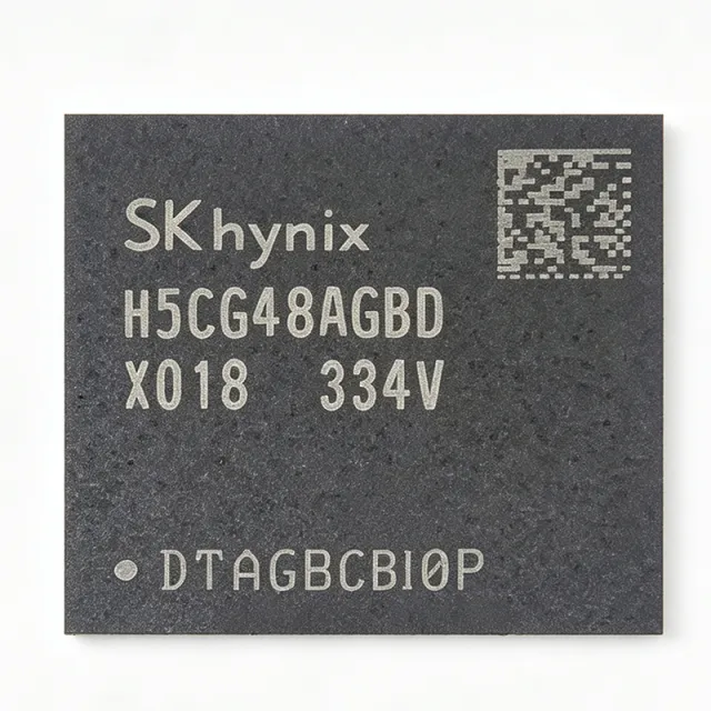
H5CG48AGBDX018N - DDR5 16Gb 5600Mbps DRAM | SK hynix
MPN: H5CG48AGBDX018N ✓ Active| Qty | Unit Price | Extended |
|---|---|---|
| 1 | $87.42 | $87.42 |
| 10 | $87.42 | $874.20 |
| 100 | $87.42 | $8,742.00 |
| 500 | $87.42 | $43,710.00 |
| 1,000 | $87.42 | $87,420.00 |
H5CG48AGBDX018N Overview
DDR5 SDRAM is the fifth generation of Double Data Rate synchronous dynamic random-access memory, a class of volatile memory ICs within the broader memory and power-management hierarchy of modern computing systems. Compared with DDR4, DDR5 doubles the bank count, moves the power management IC (PMIC) onto the memory module, reduces the per-channel word length to 16 bits, and lowers the operating voltage from 1.2V to 1.1V, which together raise bandwidth and improve power efficiency for servers, workstations, and AI computing platforms.
Key features of the H5CG48AGBDX018N include the 16Gb (2G x 8) single-die density, DDR5-5600 speed grade with an 8-bit data bus width, and a nominal 1.1V core supply that reduces dynamic power versus DDR4-class parts. The x8 organization simplifies memory controller configuration for embedded and module designs, and the device is rated for operation across a -40C to +85C temperature range per distributor data, supporting industrial environments in addition to consumer and computing applications.
Technically, the part is manufactured on SK hynix advanced DRAM process technology (the A-die generation per cross-reference sources) and follows the JEDEC DDR5 SDRAM standard interface, including on-die ECC support, decision-feedback equalization (DFE) on the DQ receivers, and an I3C-based sideband bus for host control, all standard characteristics of the DDR5 generation. These features maintain signal integrity at 5600 Mbps pin speeds on conventional PCB stackups.
Typical applications include server main memory, AI and high-performance computing modules, industrial controllers requiring firmware boot and embedded logging memory, computing modules and consumer electronics, and replacement sourcing for DDR5-based BOM lines.
A key design consideration: DDR5 does not run from a fixed 1.1V rail in module designs - the on-module PMIC regulates the rail, so discrete (solder-down) designs must provide a dedicated 1.1V supply with proper decoupling and follow JEDEC fly-by routing for CA and DQ signals.
This page synthesizes distributor pricing, drop-in alternatives, design notes, and lifecycle context not consolidated in the manufacturer datasheet.
Drop-in alternatives for H5CG48AGBDX018N — same package, pin-to-pin compatible. Different-package parts requiring PCB rework are excluded.
Variants in this series
Same-series models that are drop-in compatible with H5CG48AGBDX018N (same form factor and footprint) — differing in Package, Interface, Data Rate, Organization, Density.
Quick Comparison Tool — Select alternative parts for side-by-side comparison:
H5CG48MEBDX014N
✓ In Stock
$41.68 / Unit
View Datasheet →H5CG48AGBDX018
✓ In Stock
$63.9844 / Unit
View Datasheet →K4RAH086VB-BCQK
✓ In Stock
$41.0156 / Unit
View Datasheet →MT62F3G32D8DV-023
✓ In Stock
$55.7 / Unit
View Datasheet →H5CG48AGBDX018N Maximum Ratings & Electrical Characteristics
| Memory Type | DDR5 SDRAM |
| Density | 16 Gb (2G x 8) |
| Organization | 2G x 8 |
| Data Rate | 5600 Mbps |
| Supply Voltage | 1.1 V |
| Bus Width | 8 bit |
| Package | 82-ball FCBGA (JEDEC DDR5 78/82-ball) |
| Mounting Type | Surface Mount |
| Operating Temperature | -40C to +85C |
| Interface | JEDEC DDR5 |
| Memory Generation | DDR5 (SK hynix A-die) |
| Clock Frequency | up to 5600 MHz (data rate 5600 Mbps) |
| Application Class | Computing, industrial controllers, embedded logging |
H5CG48AGBDX018N 82-ball fcbga (jedec ddr5 78/82-ball) Pin Configuration Guide
Pin configuration for H5CG48AGBDX018N (82-ball fcbga (jedec ddr5 78/82-ball) package). This digital IC includes GPIO, communication interfaces (UART, SPI, I2C), and power pins. Refer to the manufacturer datasheet for alternate pin functions and configuration options. Essential for embedded system design and PCB layout.

No detailed pinout data available for H5CG48AGBDX018N.
Refer to the datasheet for full pin configuration.
Typical Applications
H5CG48AGBDX018N is suitable for 6 applications: Server Main Memory, AI and High-Performance Computing Modules, Industrial Controllers and Edge Systems, Embedded Firmware Boot and Logging Memory, Consumer Electronics and Computing Systems, Replacement Sourcing and BOM Risk Mitigation.
Server Main Memory
Data center servers rely on DDR5-class DRAM for their combination of bandwidth, density, and power efficiency, and the H5CG48AGBDX018N fits this role directly with 16Gb density, 2Gx8 organization, and 5600 Mbps data rate. In solder-down server designs or RDIMM-style modules, the x8 organization simplifies ECC implementation since error-correction can be computed over single x8 devices, and the 1.1V rail cuts per-bit dynamic power versus DDR4 at comparable bandwidth. Placed in a fly-by-routed DDR5 channel with the controller DFE equalization enabled, this part sustains 5600 Mbps signaling on conventional PCB stackups. Thermal design should target airflow across the FCBGA balls, as sustained near-peak bandwidth at elevated ambient temperature may require 2x refresh mode.
Recommended
AI and High-Performance Computing Modules
AI accelerator and HPC compute modules demand maximum memory bandwidth close to the processor, and the H5CG48AGBDX018N's 5600 Mbps pin speed on the JEDEC DDR5 interface delivers high aggregate bandwidth when multiple devices are ganged per 64-bit or 128-bit channel. The A-die 16Gb density allows compact solder-down arrays - eight devices provide 16 GB per channel group - within the thermal envelope of compute modules. Because DDR5 moves the PMIC to the memory subsystem, module designers should pair this DRAM with a dedicated DDR5 PMIC and follow JEDEC fly-by clocking for training stability. The -40C to +85C industrial rating adds margin for high-power operation where local board temperatures rise above consumer norms.
Recommended
Industrial Controllers and Edge Systems
Industrial controllers benefit from the H5CG48AGBDX018N's -40C to +85C operating range, a wider window than typical consumer DDR5, which is essential for factory-floor and outdoor edge equipment facing temperature extremes. The 16Gb 2Gx8 density supports embedded logging and data buffering workloads common in automation and test systems, while the 1.1V supply keeps thermal budgets modest in sealed enclosures with passive cooling. In solder-down designs, the JEDEC DDR5 78/82-ball FCBGA footprint allows compact memory placement near the SoC, shortening trace lengths and improving signal integrity at 5600 Mbps. Designers should implement the JEDEC-recommended DQ/CA length matching and provide a dedicated regulated 1.1V rail with local decoupling since no on-board PMIC exists in discrete designs.
Recommended
Embedded Firmware Boot and Logging Memory
Systems that use DRAM as runtime storage for firmware boot staging, embedded logging, and high-cycle data capture can deploy the H5CG48AGBDX018N where 2 GB-class volatile buffering is needed alongside NAND flash. The 16Gb single-die density in one 82-ball FCBGA device minimizes board area versus stacking multiple lower-density parts, and the DDR5 interface provides burst bandwidth adequate for rapid log dumps and boot-image decompression. Pairing this DRAM with SPI NOR flash for persistent boot code is a common architecture; the DRAM holds the decompressed runtime image while the NOR provides non-volatile startup storage. Memory controllers should configure on-die ECC to protect logging data integrity over long uptime periods.
Recommended
Consumer Electronics and Computing Systems
Desktop platforms, mini-PCs, set-top boxes, and gaming peripherals that use solder-down (memory-on-board) DRAM can adopt the H5CG48AGBDX018N to reach DDR5-5600 performance without SO-DIMM connectors, saving height and cost in thin form factors. The 2Gx8 organization allows flexible channel configurations from a single x8 device to 64-bit ganged arrays, and the 1.1V operation directly improves battery-run time in portable computing designs versus 1.2V DDR4. Consumer SoCs with integrated DDR5 controllers typically auto-train this class of device at boot, so integration effort is low. Designers should still verify speed-grade support (5600 Mbps) in the SoC memory compatibility list, or fall back to the 4800 Mbps M-die variant where needed.
Recommended
Replacement Sourcing and BOM Risk Mitigation
The 2026 DDR5 allocation environment has made the H5CG48AGBDX018N a constrained line item on many BOMs, driving demand for validated replacement paths. Cross-reference resources published in 2026 identify the SK hynix H5CG48MEBDX014N (4800MT/s M-die) as a strategic pin-compatible drop-in in the identical 82-ball FCBGA package, and the Samsung K4RAH086VB-BCQK as the leading cross-brand 16Gb DDR5 x8 counterpart under the same JEDEC DDR5 78/82-ball footprint. For BOM resilience, qualify both alternatives now: run memory-controller training validation and burn-in at your target temperature before a shortage forces an unvalidated swap. Stock levels tracked across distributors exceeded 50,000 pieces as of early September 2026.
Recommended
Recommended Products Summary
Engineering reference data for H5CG48AGBDX018N — comparison, design guidance, and compliance information.
Selection Guide
Comparison with Alternatives
| Parameter | This Product | H5CG48MEBDX014N | H5CG48AGBDX018 | K4RAH086VB-BCQK | MT62F3G32D8DV-023 |
|---|---|---|---|---|---|
| Package | 82-ball FCBGA (DDR5) | 82-ball FCBGA (DDR5) - same | 82-ball FCBGA (DDR5) - same | 82-ball FCBGA (DDR5) - same | 200-ball FBDGA - different (not drop-in) |
| Brand | SK hynix | SK hynix | SK hynix | Samsung Electronics | Micron Technology |
| Density | 16 Gb | 16 Gb | 16 Gb | 16 Gb | 24 Gb |
| Organization | 2G x 8 | 2G x 8 | 2G x 8 | 2G x 8 | 3G x 32 |
| Supply Voltage | 1.1 V | 1.1 V | 1.1 V | 1.1 V | 1.1 V |
Key Differentiators
- Highest speed grade in the 16Gb DDR5 x8 drop-in group (vs H5CG48MEBDX014N)
- Extended industrial temperature range (vs K4RAH086VB-BCQK)
- Single-die 16Gb density in one 82-ball package (vs H5CG48AGBDX018)
- Trade-off: higher cost per Gb than M-die (vs H5CG48MEBDX014N)
Design Notes
In discrete (solder-down) DDR5 designs there is no on-board PMIC, so you must generate a dedicated 1.1V VDD rail for the H5CG48AGBDX018N. Estimate: eight devices at typical DDR5-5600 active currents of several hundred mA each imply an aggregate rail of multiple amps - size the regulator with at least 30% headroom. Place bulk capacitance (22-47 uF group) near the regulator and 0.1 uF ceramics at each ball group to suppress di/dt droop during burst accesses.
Follow JEDEC DDR5 fly-by routing for clock/command/address and length-matched DQ/DBI groups per the manufacturer layout guidelines. At 5600 Mbps, DQ trace length matching within a few mils and controlled impedance (approximately 40 ohms single-ended typical DDR5 practice) are required for training stability. Use a solid reference plane under all DDR5 signals and avoid splitting return paths across the FCBGA ball field.
Estimated: sustained 5600 Mbps operation with continuous read/write traffic raises junction temperature above ambient by a modest margin for a single FCBGA die, but ganged arrays of 8-16 devices concentrate heat in one board region. Target airflow or a spreader over the memory array when ambient exceeds 60C, and configure 2x refresh mode above 85C per DDR5 standard practice. Verify with thermal imaging during memory stress testing.
Do not assume cross-generation compatibility: DDR4 controllers cannot train DDR5 devices, so the H5CG48AGBDX018N cannot replace DDR4 parts on an existing board. When substituting the H5CG48MEBDX014N (4800 Mbps M-die) or Samsung K4RAH086VB-BCQK for this A-die part, re-run controller memory training and verify speed-grade support in firmware - the footprint is identical but timing tables differ.
Compliance Information
Compliance declarations were not present in the captured distributor data. Request RoHS/REACH certificates of conformance from SK hynix or XAIPART with your RFQ.



