DC-DC Converters
Products (207)
TPS53622RSBT - VR13 Dual-Channel D-CAP+ Controller | TI
The Texas Instruments TPS53622RSBT is a fully VR13 SVID-compliant dual-channel step-down controller designed for server VCCIO and VMCP rails. It supports 2+0 or 1+1 phase configurations and integrates non-volatile memory (NVM) and a PMBus interface for flexible configuration and telemetry. The device provides two outputs suitable for Intel VR13 processor power delivery, packaged in a 40-pin WQFN (RSB, 5x5 mm) package rated from -40C to 125C. A step-down controller is a power management IC that generates a regulated output voltage lower than its input by driving external power stage MOSFETs. It sits in the voltage regulator hierarchy as the control brain of a multiphase buck converter, converting the 12V server bus into low-voltage core, I/O, and memory rails. The TPS53622 uses D-CAP+ architecture with undershoot reduction (USR), delivering fast transient response, low output capacitance, and good current sharing without external loop compensation. Key features include dual-channel operation in 2+0/1+1 phase configurations, built-in NVM for storing configuration settings, and a PMBus interface for telemetry and control. The controller is fully compatible with TI NexFET power stages such as the CSD95490Q5MC, enabling high-efficiency, highly integrated power conversion solutions with minimal external component count. The TPS53622 integrates SVID logic, allowing direct communication with Intel VR13 processors. Its D-CAP+ control loop provides excellent load transient performance, critical for modern CPUs with rapidly changing current demands. NVM storage reduces boot time and ensures consistent behavior across power cycles, while PMBus enables real-time monitoring of voltage and current for system optimization. Typical applications include server VCCIO and VMCP rails, high-performance computing, data center power delivery, and storage systems. A TI reference design demonstrates 12V input to 1V output at 40A using two CSD95490Q5MC power stages. When designing with the TPS53622, ensure proper layout of the power stage and decoupling capacitors to minimize parasitic inductance, and follow TI's VR13 reference designs for SVID timing compliance.
TPS53624 - Dual-Phase D-CAP+ Buck Controller | Texas Instruments
The Texas Instruments TPS53624 is a dual-phase step-down DC-DC buck controller with integrated gate drivers, packaged in a thermally enhanced, RoHS-compliant 40-pin VQFN (6x6 mm) and rated for operation from -10C to +105C. It targets point-of-load power conversion in servers, storage, networking, and telecom infrastructure. A step-down (buck) controller is a type of switching voltage regulator that converts a higher input voltage to a lower output voltage using MOSFETs, an inductor, and a feedback control loop. Within the power management IC hierarchy, the TPS53624 sits at the controller level - it integrates the control loop and gate drivers but requires external power MOSFETs, giving designers flexibility to scale output current beyond what integrated converters achieve. Key features include the D-CAP+ control architecture, which enables fast transient response with low output capacitance, and OSR (oversampled ripple regulation) for tight regulation with low-ESR output capacitors. The PCNT pin allows selection between dual-phase and single-phase operation, optimizing light-load efficiency versus full-load capability. An integrated 8-bit DAC sets the output voltage digitally, and TI Eco-mode supports high efficiency at light loads. Technically, the dual-phase topology interleaves two switching phases, reducing input and output ripple current, allowing smaller passives, and spreading thermal dissipation across two MOSFET pairs. With integrated drivers, the part eliminates external driver ICs, shortening the gate loop and improving switching behavior. Output voltage, current limit, and switching behavior are programmed via pin straps and the voltage DAC, minimizing external component count. Typical applications include CPU and ASIC core power rails, DDR memory VDDQ supplies, network switch and router POL rails, and distributed 12V bus point-of-load conversion where a controller plus discrete FETs offers the best cost-per-amp. Design tip: keep the gate-drive loops short to the integrated drivers, size the inductor per datasheet recommendations, and use PCNT phase selection deliberately - single-phase saves quiescent power at light loads but doubles per-phase current stress at peak load.

TPS53632 - 3-2-1 Phase D-CAP+ Step-Down Controller | TI
The Texas Instruments TPS53632 is a 3-2-1 phase D-CAP+ step-down driverless controller designed for low-voltage, high-current point-of-load applications. It integrates control logic and gate-drive functions for external power stages in a 32-pin VQFN (4x4 mm) package, eliminating separate driver ICs and reducing BOM count and board area. A step-down (buck) controller is a switching DC-DC converter that regulates a lower output voltage from a higher input rail. Within the power management IC hierarchy, the TPS53632 sits in the voltage regulator > DC-DC converter > multiphase controller family. Its flexible 3-2-1 phase configuration lets designers scale output current while balancing efficiency and thermal performance, and dynamic phase add/drop optimizes light-load efficiency. Key features include the D-CAP+ control architecture, which delivers fast transient response, lowest output capacitance, and high efficiency. The standard I2C Rev 3.0 serial interface enables dynamic output voltage control (dynamic voltage scaling) and current-monitor telemetry for advanced power management. Integrated protection includes overcurrent, overvoltage, and thermal shutdown, supporting robust operation in computing environments. Technically, the driverless architecture pairs the controller with external smart power stages or discrete MOSFETs, giving designers flexibility in current rating and cost. Telemetry via I2C enables real-time load-current reporting, useful for server power capping and health monitoring. Typical applications include server and datacenter VRM power supplies, networking and telecom equipment, storage systems, and high-performance computing core rails (for example, 12V or 5V input down to processor, FPGA, and ASIC core voltages). When designing with the TPS53632, prioritize a clean power-stage layout: keep high-current switching loops short, place decoupling close to the pins, and provide generous copper area for thermal relief. The I2C bus needs pull-up resistors and correct address pin configuration. Pricing varies by distributor, with LCSC listing TPS53632RSMR from about $6.27 as of 2026-08-29.

TPS53632GRSMT - 48V GaN Half-Bridge D-CAP+ Controller | TI
The Texas Instruments TPS53632GRSMT is a half-bridge PWM controller with D-CAP+ architecture, optimized for 48-V GaN-based DC/DC converters in a 32-pin VQFN (RSM) 4x4 mm package with exposed pad. It performs single-stage conversion directly from a 48-V bus, providing fast transient response, minimal output capacitance, and high efficiency. A DC/DC switching controller is a power management IC that regulates output voltage by driving external power switches (here, GaN FETs) through a feedback-controlled PWM loop. Within the power-management hierarchy, the TPS53632G sits in the switching controller family above simple buck converters, targeting LLC-like half-bridge topologies for high-voltage server and telecom power systems. Key features include D-CAP+ control for ultra-fast load transients without complex loop compensation, an I2C Rev 3.0 interface for dynamic output voltage control and current-monitor telemetry, and compatibility with TI GaN power stages for 48-V input conversion. FindIC lists conversion from 2.5 V to 24 V control supply with a step-down single output of 0.5 V to 1.52 V at up to 60 A, making it well suited to low-voltage, high-current CPU/ASIC core rails fed from 48-V infrastructure. Technically, the D-CAP+ architecture combines a constant-on-time modulator with internal ripple compensation, delivering low output ripple and excellent transient behavior even with all-ceramic output capacitor banks. The I2C telemetry loop supports fault status readback, enabling power-system monitoring in datacenter and base-station designs. Typical applications include 48-V server power shelves, GaN-based point-of-load converters, telecom rectifiers, and high-density networking equipment where a single-stage 48-V-to-1-V conversion eliminates an intermediate bus converter stage, improving efficiency and power density. When designing, follow the TI datasheet layout guidelines: keep the switch-node loop compact, place GaN power stages adjacent to the controller, and use the exposed thermal pad soldered to a solid ground plane for heat spreading and EMI control.
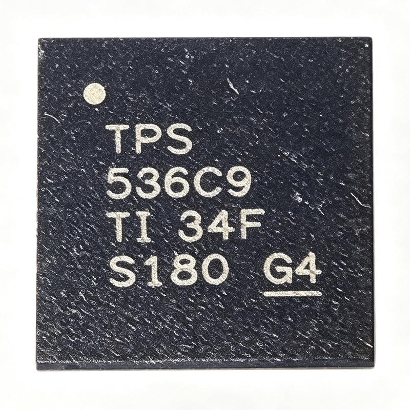
TPS536C9RSLR - Dual-Channel 12-Phase D-CAP+ Controller | TI
The Texas Instruments TPS536C9RSLR is a dual-channel, up to 12-phase step-down digital multiphase D-CAP+ controller with Intel VR14 SVID and PMBus interfaces, packaged in a thermally enhanced 48-pin VQFN (RSL) measuring 6x6 mm. It is designed for high-current, low-voltage CPU and ASIC core power conversion in servers, datacenter, and high-performance computing platforms. A multiphase buck controller is a switching-voltage-regulator controller that interleaves multiple power stages, sharing current across phases to distribute thermal load, reduce input and output ripple, and enable very fast transient response. Multiphase controllers sit at the top of the power management hierarchy, orchestrating NexFET power stages that each integrate driver and FET functions. Key features include the D-CAP+ control architecture with undershoot reduction (USR) and overshoot reduction (OSR) for fast transient response with low output capacitance; built-in non-volatile memory (NVM) for configuration storage; full PMBus command support for telemetry and control; and Intel VR14 SVID compliance for direct communication with Intel processors. The two channels (N + M) can be flexibly phase-assigned up to 12 total phases, supporting dual-rail designs such as VCORE plus VSOC. The device is fully compatible with TI NexFET power stages (such as the CSD and TPS power-stage families), enabling a complete controller-plus-power-stage solution with differential remote voltage sensing and per-phase current balance. Digital loop control provides programmable transient behavior and startup sequencing without external compensation components. Typical applications include Intel server CPU core rails (VR14), AI accelerator and GPU core power, high-current ASIC and FPGA point-of-load conversion, and storage or networking processor supplies. Design consideration: the controller requires configuration via NVM programming (TI Fusion Digital Power Designer) and careful layout of the differential remote sense lines and current-sense routing to the power stages; follow the TI datasheet layout guidelines for SW, VOSNS, and CS pins to achieve specified transient accuracy.

TPS536C9T - Dual-Channel 12-Phase D-CAP+ Controller | TI
The Texas Instruments TPS536C9T is a dual-channel (N + M <= 12 phase) D-CAP+ step-down multiphase buck controller with TLVR (trans-inductor voltage regulator) topology support, PMBus, and VR14 SVID interfaces, housed in a 48-pin VQFN (RSL) package measuring 6.00 mm x 6.00 mm with exposed pad. It operates from a 4.5 V to 17 V input range and regulates outputs down to 0.25 V, supporting up to 765 A total output current when paired with TI smart power stages. A multiphase buck controller is a power management IC that distributes a high-current step-down conversion across several interleaved phases, reducing input/output ripple, spreading thermal load, and improving transient response compared with a single-phase regulator. In the power management hierarchy, the TPS536C9T sits at the controller layer: it drives external smart power stages rather than integrating FETs, enabling server-class current levels far beyond what monolithic converters achieve. Key features include the D-CAP+ control architecture for fast transient response, low output capacitance, and strong dynamic current sharing; native TLVR support for modern CPU load-transient profiles; an integrated non-volatile memory (NVM) for pin-free configuration; and compliance with the Intel VR14 SVID specification alongside a full PMBus interface for telemetry, fault management, and runtime adjustment. Technically, the digital controller loops monitor per-phase current and temperature, and firmware-configurable parameters (stored in NVM) define phase count, switching behavior, and protection thresholds such as overcurrent, overvoltage, and overtemperature. The device is fully compatible with TI smart power stages (e.g., CSD95xxx family), simplifying design-in for multi-rail server and accelerator boards. Typical applications include VR14-compliant CPU core power for servers and workstations, ASIC/FPGA accelerator rails, high-current point-of-load conversion in networking and datacenter equipment, and 12-phase TLVR evaluation platforms such as the TPS536C7EVM-051. Design tip: because TLVR coupling and layout strongly affect transient performance, follow the TI layout guidelines for the SYNC/RESET and current-sense pins, and verify SVID boot sequencing against the platform's VR14 requirements.
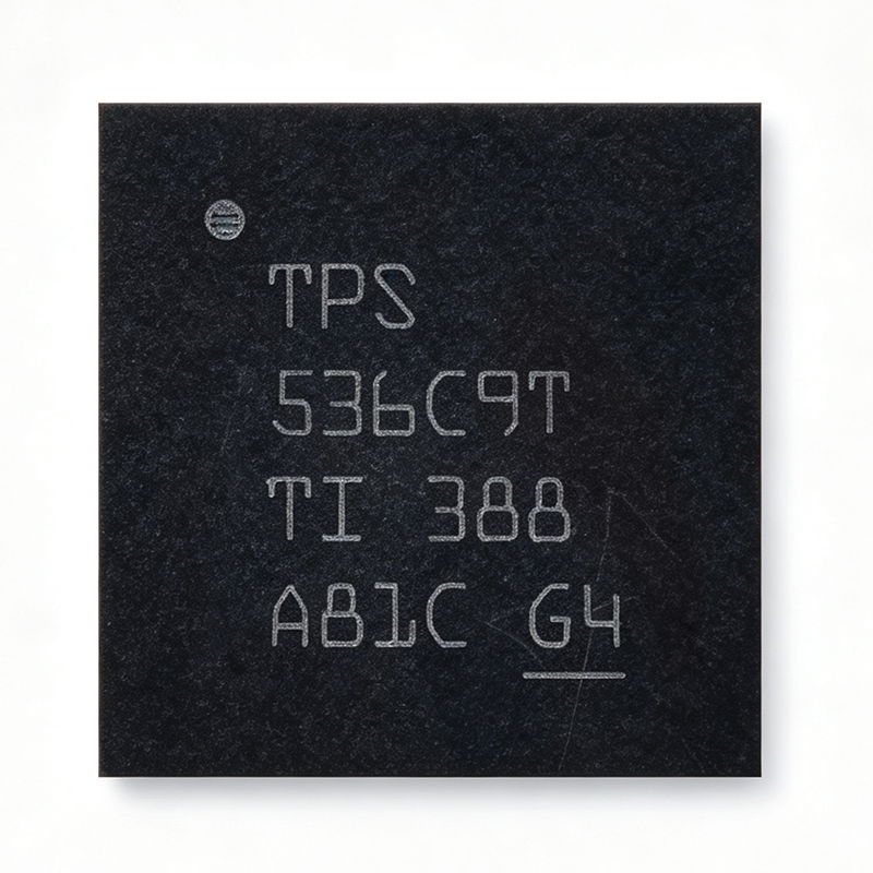
TPS536C9TRSLR - 12-Phase TLVR Buck Controller, 765A | TI
The Texas Instruments TPS536C9TRSLR is a dual-channel (N + M <= 12 phase) D-CAP+ step-down multiphase switching controller supporting up to 765A total output current in a thermally enhanced 48-pin VQFN (RSL) package with exposed pad. It supports input voltages from 4.5V to 17V and output voltages from 0.25V to 5.5V. A multiphase buck controller is a power-management IC that orchestrates multiple power stages in parallel to deliver high current at low voltage, dividing current among phases for reduced ripple, better thermal distribution, and fast transient response. The TPS536C9T sits within the hierarchy of switching regulators as a controller-class device, pairing with external TI NexFET smart power stages to form a complete voltage regulator solution (VR) for processors. Key features include native trans-inductor voltage regulator (TLVR) topology support with LC open and short protection, VR14 SVID interface compliance, and a PMBus interface for telemetry and configuration. Built-in non-volatile memory (NVM) stores configuration, and the D-CAP+ architecture provides fast transient response, low output capacitance, and accurate dynamic current sharing across phases. The controller is fully compatible with TI NexFET smart power stages, allowing flexible N+M phase allocation (N+M <= 12, M <= 6) between the two channels. This scalability suits both compact dual-rail designs and high-current single-rail configurations used by modern server CPUs and GPUs. Typical applications include server CPU core power (VR14 SVID rails), ASIC and FPGA point-of-load power, AI accelerator power delivery, and networking line-card processors requiring sub-1V, multi-hundred-amp rails with PMBus manageability. Design tip: TI recommends keeping at least 800 mil distance between controller and power stages, sharing a common ground plane, and using the PMBus/NVM configuration flow during bring-up to tune loop response before production. This page synthesizes verified datasheet parameters, drop-in alternatives, and practical design guidance not found on the manufacturer product page.
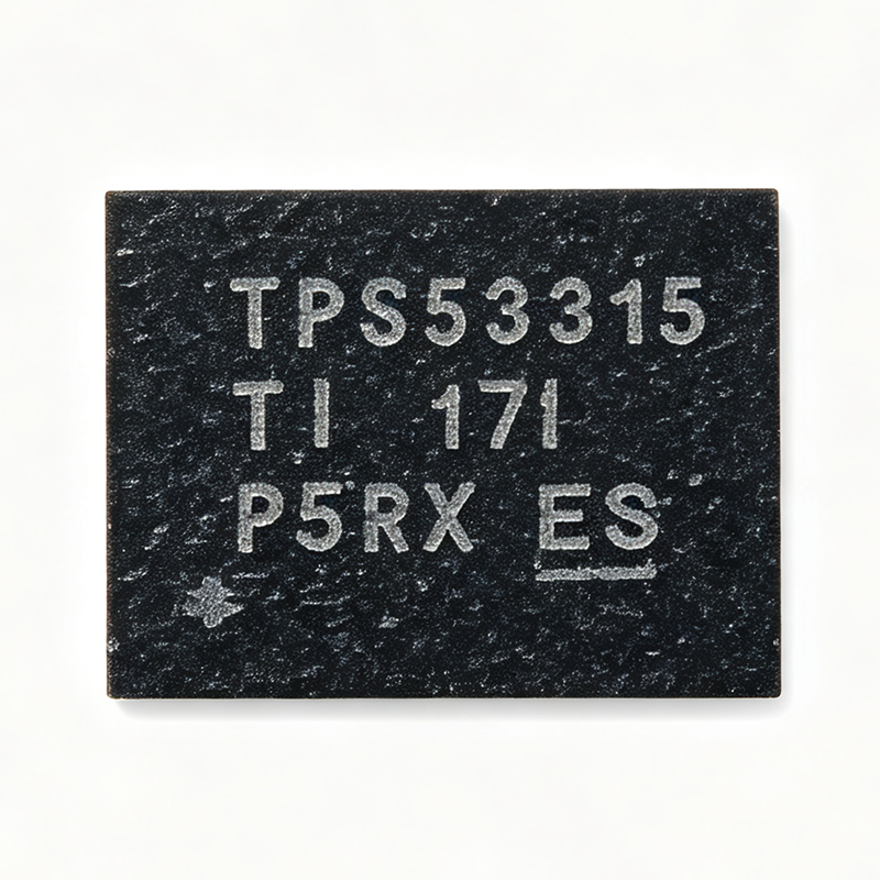
TPS53915RVER - 12A Sync Buck D-CAP3 Regulator | TI
The Texas Instruments TPS53915RVER is a 12-A synchronous step-down (buck) switching regulator with an adaptive on-time D-CAP3 control mode, supplied in a 28-pin VQFN package with exposed thermal pad. It operates from a 1.5-V to 18-V input (4.5-V to 25-V bias) and produces an adjustable 0.6-V to 5.5-V output with 0.5% reference accuracy. A synchronous buck converter is a DC/DC switching regulator that uses two internal MOSFETs plus an inductor to step a higher input voltage down to a lower, well-regulated output. Within the power management hierarchy (regulator -> switching regulator -> SWIFT point-of-load converter), buck converters deliver high efficiency compared to linear regulators because power is transferred through inductive switching rather than dissipated as heat. Key features include integrated 13.8-mOhm high-side and 5.9-mOhm low-side MOSFETs supporting 12-A continuous output current, PMBus-based configuration of voltage margining, soft-start time, power-on delay, VDD UVLO level and fault reporting, and an integrated boost switch for the high-side gate drive. The D-CAP3 adaptive on-time topology provides fast transient response with very low external component count, simplifying layouts in space-conscious systems. Technically, the TPS53915 is trimmed at the factory to enable PMBus commands with a default switching frequency of 400 kHz. The device uses a current-consuming strategy for stability with low-ESR ceramic output capacitors and supports a wide duty cycle range, making it flexible across 5-V, 12-V and intermediate bus rails down to sub-1-V core voltages. Typical applications include point-of-load power for DSPs, FPGAs and ASICs, industrial and enterprise server power rails, and telecom/datacom 12-V distributed power systems requiring fast transient response and high current density. Design tip: ensure adequate PCB copper area on the exposed pad for heat dissipation at full 12-A load, and verify PMBus resistor straps or serial configuration choices against datasheet sequencing guidance before layout. Pricing shown is as of 2026-08-29.
TPS54120 - Low-Noise 1A Buck + LDO Power Supply | TI
The Texas Instruments TPS54120 is a low-noise, 1-A integrated power supply that combines a high-efficiency step-down (buck) DC-DC converter with a high power-supply-rejection, low-dropout regulator (LDO) in a single 24-pin VQFN (RGY, 5.5 x 3.5 mm) package. The two-stage architecture delivers an ultra-low-noise regulated output for noise-sensitive analog loads while retaining the efficiency of switching conversion. An integrated power supply, or PMIC-style power stage, combines multiple regulation stages so a single IC replaces a discrete converter-plus-LDO chain. In the system power hierarchy, the TPS54120 sits within power management ICs (PMICs) -> voltage regulators -> DC-DC converters and LDO linear regulators. By cascading a buck converter with a low-noise LDO, the design attenuates switching ripple before it reaches the load, achieving far lower output noise than a buck regulator alone without the power penalty of an all-linear solution. Key features include a configurable switching frequency of 200 kHz to 1.2 MHz with frequency synchronization, adjustable soft-start for controlled inrush, power-good output for supply sequencing supervision, adjustable output voltages using external resistor dividers (down to 0.6 V reference per TI documentation conventions), and a fully configurable dc-dc and LDO stage. The high PSR of the integrated LDO stage suppresses buck ripple, making the output suitable for RF, clocking, and precision analog rails. According to the TI datasheet, typical applications include telecom infrastructure, pico and femto base stations, and powering sensitive clocking distribution where phase noise directly impacts system performance. The single-package integration reduces BOM count and board area versus a discrete two-chip solution. In design, place the buck switching loop components tightly, and give the LDO stage sufficient headroom so the LDO output stays in regulation; the LDO drop-out determines the minimum buck output setting for a clean final rail.
TPS54120 - Low-Noise 1A DC-DC + LDO Supply | TI
The Texas Instruments TPS54120 is a low-noise, 1A power supply that integrates a high-efficiency step-down DC-DC converter with a high power-supply-rejection low-dropout regulator (LDO) in a single 24-pin VQFN (5.5x3.5 mm) package. It operates from a 4.5V to 17V input, well suited to 12V power buses, with switching frequency adjustable from 200kHz to 1.2MHz. A power supply with an integrated DC-DC converter and LDO is a hybrid power management architecture within the voltage regulator family of power management ICs: the buck converter performs efficient step-down conversion, while the downstream LDO provides high power-supply rejection (PSR) and low output noise for sensitive loads. This two-stage approach in one IC eliminates the discrete two-chip design effort and is essential for powering clocking distribution, data converters, and RF circuits. Key features include adjustable output voltage up to 6.0V via external resistors, soft-start, switching-frequency synchronization to an external clock, spread-spectrum clocking (SSC) for EMI reduction, power-good output, output discharge, fixed UVLO, overcurrent protection, and synchronous rectification. The fully configurable converter and LDO allow a wide range of low-noise rail designs from a single device. Architecturally, the proprietary interaction between the buck stage and the LDO optimizes the efficiency-versus-noise trade-off: the converter handles the bulk voltage transformation, keeping LDO dropout small so PSR remains high with minimal efficiency penalty. The 24-VQFN (RGY) package provides a compact footprint with good thermal performance for space-constrained designs. Typical applications include telecom infrastructure, pico and femto base stations, and powering sensitive clocking distribution such as PLLs, VCOs, and high-speed ADCs and DACs, where clean rails directly improve phase noise and SNR. Design tip: keep the switching node short to minimize EMI, bypass the LDO output with a low-ESR ceramic capacitor for stability, and use the soft-start pin to control inrush current at power-up. Prices referenced are as of 2026-08-29.
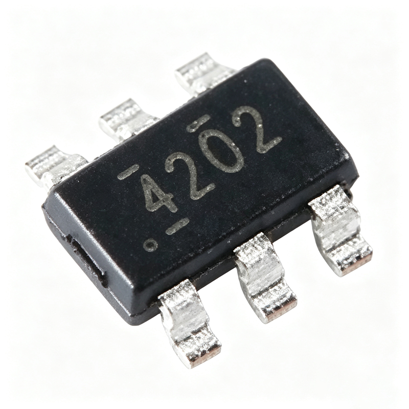
TPS54202DDCR - 4.5V-28V 2A Sync Buck Converter | TI
The Texas Instruments TPS54202DDCR is a 4.5V to 28V input, 2A synchronous step-down (buck) converter in a compact 6-pin SOT-23-THN (DDC) package. It integrates two switching MOSFETs, internal loop compensation, and a 5ms internal soft-start, drastically reducing external component count and PCB footprint for point-of-load designs. A buck (step-down) converter is a DC-DC switching regulator that efficiently converts a higher input voltage to a lower output voltage using inductive energy storage and high-frequency switching. Unlike linear regulators, buck converters achieve high efficiency even with large input-to-output voltage differentials. As a synchronous buck, the TPS54202 replaces the freewheeling Schottky diode with an integrated low-side MOSFET, improving light-load and full-load efficiency within the power management IC family. Key features include the adjustable output range of 0.596V to 26V, a fixed 500kHz switching frequency, and Advanced Eco-mode operation that folds back switching frequency at light loads to extend standby efficiency. The 45uA quiescent current suits always-on and battery-backed systems. EMI-friendly design techniques ease EMC compliance, and integrated overcurrent and thermal shutdown protection ensure robustness. The -40C to +125C junction temperature range supports industrial environments. Architecturally, the device uses current-mode control with internal compensation, so no external compensation network is needed. Integrated low-RDS(on) MOSFETs deliver high efficiency in the small SOT-23-6 thin package, achieving high power density without a heatsink at moderate loads. Typical applications include 12V and 24V rail point-of-load conversion in set-top boxes, broadband and networking equipment, industrial supplies, and portable instruments. For example, it efficiently steps 12V down to 3.3V for digital logic with minimal ripple. Design tip: follow the datasheet recommendation of a 10uF input and 22uF output ceramic capacitor, and keep the SW/BOOT loops tight on the PCB; verify thermal relief on the exposed area for loads above 1.5A.
TPS54218 - 2A, 2MHz Sync Buck Converter | TI | Point-of-Load
The Texas Instruments TPS54218 is a full-featured 6V, 2A synchronous step-down SWIFT DC-DC converter with two integrated 30-mOhm (typical) MOSFETs, packaged in a small, thermally-enhanced 3-mm x 3-mm 16-pin WQFN (RTE) exposed-pad package. It accepts an input voltage range of 2.95V to 6V and delivers an adjustable output from 0.803V at up to 2A. A DC-DC switching regulator (buck converter) is a power-management IC that converts a higher input voltage to a lower output voltage using high-frequency switching and an external inductor, achieving far higher efficiency than a linear regulator. The TPS54218 sits within the SWIFT family of point-of-load converters optimized for distributed power architectures. Key features include a programmable switching frequency from 200 kHz to 2 MHz, which reduces inductor size and solution footprint; a 0.8V voltage reference with +/-1% accuracy over temperature; current-mode control for simplified loop compensation and fast transient response; synchronization to an external clock; and adjustable soft start or power sequencing via the SS/TR pin. Under-voltage and over-voltage power-good output provides rail supervision. Efficiency is maximized by the integrated 30-mOhm MOSFETs and a typical 350-uA supply current; using the EN pin, shutdown current is reduced to 2 uA. The current-mode architecture enables small external component count and compact solutions. Up to 2-MHz operation allows the use of low-profile inductors, making the part well suited to space-constrained boards. Typical applications include point-of-load regulation for DSPs, FPGAs, and ASICs, 5V or 3.3V distributed-power rails in industrial and networking equipment, and portable/battery-connected systems needing high efficiency at 2A loads. Design tip: operating at 2 MHz reduces inductance requirements but increases switching losses; balance frequency against efficiency using the datasheet equations, and place the input capacitor, inductor, and BOOT capacitor close to the IC pins.
TPS54218ARTER - 2A, 6V Sync Step-Down Buck Regulator | TI
The Texas Instruments TPS54218ARTER is a 2 A synchronous step-down (buck) converter from the SWIFT family, operating from a 2.95 V to 6 V input with an adjustable output down to 0.803 V, packaged in a 16-pin VQFN (RTE) with exposed pad measuring 3 mm x 3 mm. A synchronous buck converter is a type of DC-DC switching regulator that replaces the freewheeling diode of a classic buck topology with an integrated second MOSFET, improving efficiency at low output voltages. Within the power-management hierarchy, it sits as a point-of-load voltage regulator IC, converting a higher intermediate bus voltage into a tightly regulated low-voltage rail for processors, FPGAs, and mixed-signal loads. Key features include two integrated n-channel MOSFETs that reduce external component count, constant-frequency peak current-mode control that simplifies loop compensation and reduces output capacitance, and a wide programmable switching-frequency range of 200 kHz to 2 MHz that permits very small inductors. The adjustable output uses a 0.803 V feedback reference. Technically, the peak current-mode architecture provides fast line and load transient response and cycles-by-cycle current limiting. The high switching capability enables single-digit-millihenry inductance values and a compact 3x3 mm power solution footprint, while integrated MOSFETs minimize switching-node parasitics. Typical applications include point-of-load power for DSPs and FPGAs, 5 V or 3.3 V distributed-bus post-regulation in industrial controls, and telecom/networking line cards where a small 2 A POL buck is needed. A key design consideration is that because this is a switching converter, PCB layout of the PH switching node, input decoupling, and ground return directly affects EMI and output ripple - keep the input capacitor loop minimal. This page synthesizes verified distributor pricing, same-family drop-in alternatives, and practical design notes beyond the raw datasheet.
TPS54218RTE - 2A, 6V, 2MHz Sync Buck Converter | TI
The Texas Instruments TPS54218RTE is a 2.95 V to 6 V input, 2 A output synchronous step-down (buck) SWIFT converter with an adjustable output voltage from 0.803 V and a switching frequency range up to 2 MHz, housed in a 16-pin WQFN package with exposed pad (RTE suffix). A synchronous buck converter is a type of DC-DC switching voltage regulator that steps a higher input voltage down to a lower output voltage using two integrated MOSFETs - a high-side and a low-side switch - instead of an external Schottky diode. This topology belongs to the broader power management IC family and delivers significantly higher efficiency than linear regulators, especially at large step-down ratios, making synchronous buck converters the workhorse of point-of-load power conversion in modern electronics. Key features of the TPS54218 include two integrated n-channel MOSFETs, which reduce external component count and board area; constant-frequency peak current mode control, which simplifies external frequency compensation and reduces output capacitance requirements; and a wide supported switching frequency range starting from 200 kHz and adjustable up to 2 MHz, allowing designers to trade efficiency against solution size. Architecturally, the peak current mode control scheme provides fast transient response to line and load changes, which is critical for powering DSPs, FPGAs, and microprocessors with dynamic load profiles. The internal MOSFETs minimize switching node parasitics for clean switching behavior, and the high frequency capability enables the use of small inductors and ceramic output capacitors for compact point-of-load designs. Typical applications include 5 V or 3.3 V rail point-of-load conversion for DSPs such as the TMS320F2803x series, general-purpose 2 A core and I/O rails in industrial control, and distributed power in networking and test equipment where a low profile, high-frequency solution is required. When designing with this device, ensure the input voltage stays within the 2.95 V to 6 V absolute operating window and select the RT-set frequency and inductance appropriate for your ripple current and transient targets. This page synthesizes distributor data, verified datasheet parameters, alternative-part context, and practical design notes in one place - information not consolidated in the manufacturer datasheet alone.
TPS54218RTER - 2A, 2MHz Sync Step-Down Buck | TI
The Texas Instruments TPS54218RTER is a 2A synchronous step-down SWIFT DC-DC buck converter with a 0.8V plus or minus 1 percent voltage reference, 2.95V to 6V input range, and an adjustable switching frequency of 200 kHz to 2 MHz, housed in a 16-pin WQFN (RTE) package with exposed pad. A synchronous buck converter is a type of switching voltage regulator that steps a higher DC input voltage down to a lower regulated output voltage using two internal MOSFETs - a high-side control FET and a low-side synchronous rectifier - instead of an external Schottky diode. Within the power management hierarchy (DC-DC converter, switching regulator, power management IC), synchronous topologies improve efficiency at light and full load by eliminating diode conduction losses, which is why they dominate point-of-load designs in modern digital systems. Key features include two integrated 30 mOhm (typical) MOSFETs delivering high efficiency at full 2A load, an externally synchronizable switching frequency from 200 kHz to 2 MHz for filter and footprint optimization, a precision 0.8V reference holding plus or minus 1 percent over temperature, and adjustable soft start with sequencing support. UV and OV power-good monitoring simplifies system supervision and fault reporting. Architecturally, the TPS54218 belongs to TI's SWIFT family of point-of-load converters. The D-CAP-style adaptive on-time control approach delivers fast transient response with low output ripple while supporting ceramic output capacitors without complex compensation. The integrated FETs and compact 16-WQFN (RTE) exposed-pad package minimize the external component count and PCB area for space-constrained rails. Typical applications include 5V or 3.3V point-of-load conversion for DSPs, FPGAs, and ASICs; DDR memory rail generation in networking and telecom equipment; and low-voltage rail powering in industrial and consumer systems where the narrow 2.95V to 6V input aligns with 3.3V and 5V intermediate bus rails. When designing, select the inductor and output capacitor for the chosen switching frequency: at 2 MHz, smaller inductance values reduce solution size but increase ripple current, while operating near 200 kHz maximizes efficiency. Keep the PH and BOOT loops tight and use the exposed pad as the thermal ground. This page synthesizes verified distributor pricing, drop-in alternative analysis, pinout guidance, and practical design notes not consolidated in the manufacturer datasheet.
TPS54283 - Dual 2A 300kHz Buck Converter | Texas Instruments
The Texas Instruments TPS54283 is a dual-output, non-synchronous buck (step-down) converter that integrates a high-side MOSFET and is rated for up to 2 A per channel. It operates from a 4.5-V to 28-V input supply, and each output is adjustable from 0.8 V up to 90% of the input voltage. The device switches at a fixed 300 kHz with internal compensation, and is offered in a 14-pin PowerTSSOP (HTSSOP-14, PWP) surface-mount package with an exposed PowerPAD for heat removal. This makes it a compact two-rail power solution for networking, consumer, and industrial boards. What is a non-synchronous buck converter? A non-synchronous buck converter is a step-down switching regulator that uses an integrated high-side MOSFET as the control switch and an external Schottky diode as the low-side rectifier. Because the TPS54283 integrates the high-side switch, each of its two channels only needs an external Schottky diode, an inductor, and input/output capacitors. In the power management hierarchy it is: DC-DC converter -> non-synchronous buck converter -> step-down switching voltage regulator -> power management IC. Key features include dual 2-A outputs, a wide 4.5-V to 28-V input range, adjustable output down to 0.8 V, fixed 300-kHz switching, internal compensation, and an integrated high-side MOSFET. The internal error-amplifier compensation removes the external compensation network, reducing BOM count and simplifying loop-stability design. The wide input range gives margin for 5-V, 12-V, and 24-V systems. From a technical standpoint, the current-mode controlled converter balances inductor size, output ripple, and efficiency at 300 kHz. Because the low-side rectifier is external, a designer can optimize the Schottky diode for forward voltage and thermal behavior. The PowerPAD must be soldered to a solid ground-plane copper area to keep junction temperature within limits at full dual 2-A load. Typical applications include broadband gateways (DSL/cable modems), IP security cameras, set-top boxes, and industrial control boards that generate a 5-V and a 3.3-V rail from a 12-V or 24-V input. The adjustable output also supports point-of-load power in consumer media devices. When designing with the TPS54283, verify input-to-output headroom and Schottky diode rating for each channel, and use the exposed thermal pad to a large ground copper pour. Total dissipation is the combined loss of both channels, so thermal layout is critical at 2 A per output.

TPS54302DDCR - 3A 4.5-28V Sync Buck | Texas Instruments
The Texas Instruments TPS54302DDCR is a 4.5V to 28V input, 3A output, EMI-friendly synchronous step-down converter in a 6-pin SOT-23-6 Thin (TSOT-23-6, DDC) package. It integrates two switching N-channel MOSFETs, internal loop compensation, and a 5ms internal soft start, reducing external component count for point-of-load power-supply design. The adjustable output reaches down to a 0.596V reference, covering 3.3V, 5V, and low-voltage core rails for FPGAs, MCUs, and SoCs. A synchronous buck converter is a DC-DC switching regulator in which a high-side and a low-side power FET switch alternately to convert a higher input voltage to a lower regulated output with high efficiency. It belongs to the switching regulator family within the power management IC hierarchy. Because the low-side FET replaces the Schottky diode of asynchronous converters, conduction losses drop and heavy-load efficiency improves significantly. The TPS54302 uses constant-frequency peak current-mode control at approximately 400kHz, providing fast line and load transient response and reducing required output capacitance. Key features include 3A continuous output current, a wide 4.5V to 28V input range, and a 5ms internal soft start that limits inrush current at power-up. Advanced Eco-mode delivers high light-load efficiency, and the EMI-friendly switching-edge design reduces the need for extra filtering in noise-sensitive products such as wireless IoT gateways. The TSOT-23-6 package occupies minimal board area and supports reflow up to 260C. Typical applications include industrial 24V and 12V rails, set-top boxes, battery-powered portable equipment, networking hardware, smart-home IoT gateways, and LED display control power. The wide input range plus 3A output make it a versatile point-of-load regulator, and the EMI-friendly design is valuable wherever RF sensitivity could be degraded by switching noise. Design tip: place input and output ceramic capacitors close to the IC, choose a power inductor with saturation current above 3.2A, and set the output voltage with 1% tolerance resistors on the 0.596V reference. Since 28V is the maximum rating, add transient protection if input spikes above 28V are possible.

TPS54302QDDCRQ1 - 28V 3A Sync Buck AEC-Q100 | TI
The Texas Instruments TPS54302QDDCRQ1 is an AEC-Q100 qualified, 4.5V to 28V input, 3A synchronous step-down (buck) converter in a compact 6-pin SOT-23-6 Thin (DDC) package. The device integrates two switching MOSFETs (85 mOhm high-side, 40 mOhm low-side), internal loop compensation, and a 5 ms internal soft start, drastically reducing external component count and solution size. A synchronous buck converter is a type of DC-DC switching voltage regulator that replaces the catch diode of a conventional buck regulator with an integrated low-side MOSFET, achieving higher efficiency, especially at light load and low duty cycle. Within the power management IC hierarchy, it belongs to the family of step-down regulators used to derive low-voltage, high-current rails from higher-voltage industrial or automotive supplies. Key features include a fixed 400 kHz switching frequency, frequency spread spectrum and EMI-friendly layout that reduce conducted and radiated emissions, Advanced Eco-mode pulse-skip operation for excellent light-load efficiency, and peak current-mode control for simple, stable loop behavior. The very low 2 uA shutdown current and 45 uA quiescent current suit battery-backed and always-on automotive systems. The adjustable output voltage is set down to 0.596V via a resistor divider. Technically, the peak current-mode architecture with internal compensation eliminates the need for loop tuning, while integrated bootstrap diode and dead-time control improve robustness. The AEC-Q100 qualification and wide input range make the device resilient against automotive load-dump clamped rails (12V/24V battery systems) and 24V industrial buses. Typical applications include automotive infotainment and cluster point-of-load power, ADAS sensor module supplies, 24V industrial automation rails, and telecom/medium-voltage sub-rails where EMI compliance matters. Design consideration: with a 3A continuous output, thermal performance depends on the SOT-23-6 copper area; follow the TI datasheet layout recommendations for the thermal pad and input capacitor placement, and keep switching-node area small to exploit the EMI-friendly design.
TPS5430DDAR - 3A, 36V Step-Down Converter | Texas Instruments
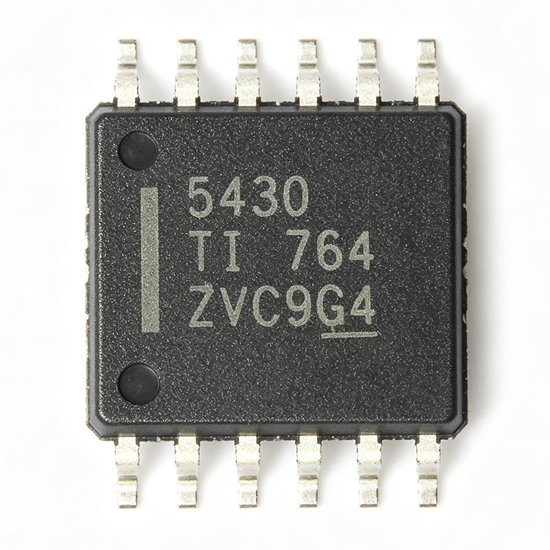
The Texas Instruments TPS5430DDAR is a 3A, wide-input step-down (buck) DC-DC converter in an 8-pin SO PowerPAD (DDA) package. It accepts 5.5V to 36V input and delivers an adjustable output from 1.221V up to near VIN at a fixed 500kHz switching frequency. A buck converter is a type of switching voltage regulator that efficiently steps a higher DC voltage down to a lower one using a switching MOSFET, an inductor, and output capacitors. Unlike linear regulators, switching converters routinely exceed 90% efficiency, making them the foundation of modern power management IC hierarchies (DC-DC converter -> switching regulator -> point-of-load converter). The TPS5430 belongs to TI's SWIFT family of DC-DC converters. Key features include the 5.5V to 36V input range that directly accepts 12V and 24V industrial and automotive buses, 3A continuous output current, fixed 500kHz operation that permits small inductors, an integrated high-side N-channel MOSFET, internal loop compensation, soft-start, cycle-by-cycle current limit, and thermal shutdown. The thermally enhanced SO-8 PowerPAD package provides low thermal resistance for full-load operation without an external heatsink. The device uses PWM voltage-mode control with an internal 1.221V bandgap reference; output voltage is set by an external resistor divider on the VSENSE pin. A bootstrap capacitor between BOOT and PH drives the high-side MOSFET gate above VIN. Fixed-frequency operation simplifies EMI filter design compared with variable-frequency converters. Typical applications include point-of-load supplies for FPGAs, DSPs, and microcontrollers, 24V industrial bus power, telecom intermediate rails, 12V automotive accessory power, and 5V/3.3V distributed power systems. Design tip: place input/output capacitors and the bootstrap capacitor close to the IC, solder the PowerPAD to a copper pour with thermal vias, and keep the PH switching node and power loops short to minimize ringing and EMI.
TPS5430QDDARQ1 - 3A, 36V Buck Converter AEC-Q100 | TI
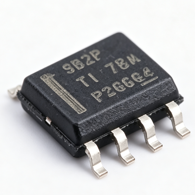
The Texas Instruments TPS5430QDDARQ1 is an automotive-qualified (AEC-Q100) 3A step-down (buck) switching regulator from the SWIFT family, operating from a wide 5.5V to 36V input range at a fixed 500kHz switching frequency in a thermally enhanced 8-pin HSOIC (DDA) PowerPAD package rated from -40C to +125C. A DC-DC buck converter is a type of switching voltage regulator that steps a higher DC input voltage down to a lower regulated output voltage using a high-side switch, an inductor, and a rectifying element. Buck converters sit within the broader hierarchy of power management ICs and, unlike linear regulators, achieve high efficiency by switching rather than dissipating excess power as heat. Key features include up to 3A continuous output current, an adjustable output voltage from 1.221V to approximately 31V, voltage-mode PWM control with an integrated low-resistance high-side N-channel MOSFET, and non-synchronous rectification using an external Schottky diode. The 500kHz fixed frequency permits a compact inductor, while the internal compensation minimizes external component count. The PowerPAD package provides low thermal resistance for high-power-density designs. According to the TI TPS5430-Q1 datasheet, the device integrates cycle-by-cycle current limiting, thermal shutdown, and an enable pin for rail sequencing. WEBENCH support and evaluation modules accelerate design cycles. The wide 36V input withstands automotive load-dump transients with modest protection, supporting battery-direct connections in 12V and 24V systems. Typical applications include automotive infotainment and cluster power supplies, USB charging ports from battery rails, industrial 24V auxiliary supplies, and 5V/3.3V point-of-load conversions for MCUs and CAN transceivers. Design consideration: because the converter is non-synchronous, select an external Schottky diode rated for the full output current and peak switch current, and keep the PH node loop as small as possible for low EMI.

TPS54331DR - 3A 28V Buck Converter 570kHz | Texas Instruments
The Texas Instruments TPS54331DR is a 28V, 3A non-synchronous buck converter integrating a low RDS(on) high-side MOSFET. It operates from 3.5V to 28V input and provides an adjustable output from 0.8V to 25V in an 8-pin SOIC (D) package. A buck converter, or step-down converter, is a DC-DC switching regulator that efficiently reduces a higher input voltage to a lower output voltage. Unlike linear regulators, buck converters use switching elements and an external inductor to transfer energy, achieving high efficiency especially at large input-to-output voltage differences. The TPS54331DR is a non-synchronous buck converter within the broader power management IC family, using an external diode for low-side rectification, which simplifies design and reduces cost compared to synchronous converters. Key features include a fixed 570kHz switching frequency, current mode control with internal slope compensation, and Eco-mode pulse-skipping that improves light-load efficiency. The device offers 1uA shutdown supply current for battery-powered applications, adjustable soft-start, cycle-by-cycle overcurrent protection, and thermal shutdown. The integrated high-side MOSFET minimizes conduction losses. Architecturally, current mode control compares the COMP pin voltage to the switch current each cycle to turn off the high-side MOSFET. This provides excellent line and load transient response and simplifies external compensation. Eco-mode automatically reduces switching frequency at light loads, maintaining efficiency across wide load ranges. Typical applications include industrial power supplies, set-top boxes, LCD displays, distributed power systems, and consumer electronics. Its wide input range and 3A output make it ideal for powering FPGAs, DSPs, and microcontrollers from 12V or 24V buses, with output set precisely via external resistors. Design tip: ensure proper input/output capacitor selection and a tight PCB layout to minimize parasitic inductance. The COMP pin requires an external RC network for loop compensation, and the bootstrap capacitor must sit close to the BOOT pin for reliable high-side gate drive.

TPS54331DRCR - 3A 28V Step-Down Buck Converter | TI
The Texas Instruments TPS54331DRCR is a 28V-input, 3A non-synchronous step-down (buck) DC-DC converter with a fixed 570kHz switching frequency, adjustable output from 0.8V to 25V, and Eco-mode pulse-skipping for light-load efficiency, housed in an 8-pin SOIC (D) surface-mount package. According to TI, the device integrates a low RDS(on) high-side MOSFET and operates from a 3.5V to 28V input rail. A buck (step-down) converter is a switching voltage regulator that converts a higher DC input voltage to a lower regulated output voltage using a switching element, inductor, and output capacitor. Buck regulators sit within the broader hierarchy of power management ICs: switching regulator > DC-DC converter > voltage regulator. Compared to linear regulators (LDOs), buck converters achieve far higher efficiency, often above 90 percent, making them the default choice whenever the input-to-output voltage differential is large or load currents exceed roughly 500mA. Key features of the TPS54331 include the Eco-mode feature that automatically activates pulse-skipping at light loads to maintain high efficiency, and an ultra-low 1uA shutdown supply current that suits battery-powered applications. Current-mode control with internal slope compensation simplifies loop compensation design and delivers fast transient response. A fixed 570kHz switching frequency keeps the power inductor and capacitors small and places switching noise above most sensitive audio and RF bands. Technically, the converter is a non-synchronous (external free-wheel diode) topology, which keeps the IC cost low while requiring a Schottky diode such as the B340A on the PH switch node. The integrated 3A MOSFET, internal soft-start via SS/TR pin, programmable EN pin with hysteresis, and COMP pin for external loop compensation give designers full control over startup, efficiency, and transient behavior. Wide 3.5V to 28V input range covers 5V, 12V, and 24V industrial rails. Typical applications include 12V and 24V industrial auxiliary power rails, 5V or 3.3V point-of-load supplies for MCUs and FPGAs, LED lighting drivers, battery-powered instrumentation, and networking equipment. The 3A rating comfortably powers embedded processors, motors control logic, and multi-rail distributed power systems. For design, choose the free-wheel Schottky diode for low forward voltage and adequate current rating, keep the PH loop area small, and set the compensation network per the datasheet equations for your output capacitor ESR. Verify junction temperature with the SOIC-8 thermal metrics for your copper area. This page synthesizes verified distributor pricing, drop-in alternatives including the TI TPS54332D pin-for-pin replacement and the cross-brand SGM61232XG, plus practical design notes not found in the manufacturer datasheet.

TPS54335ADRCR - 4.5-28V In, 3A Sync Buck Converter | TI
The Texas Instruments TPS54335ADRCR is a 3 A synchronous step-down (buck) DC-DC converter with 4.5 V to 28 V input range, adjustable output from 0.8 V, and Eco-mode light-load efficiency, housed in a 10-pin VSON (DRC) package with exposed pad. A synchronous buck converter is a switching voltage regulator that uses high-side and low-side MOSFETs (instead of a diode) to step a higher input voltage down to a lower, tightly regulated output. Within the power management IC hierarchy, the TPS54335A sits in the switching regulator family, which achieves far higher efficiency than linear regulators (LDOs) because energy is transferred in switched inductor cycles rather than dissipated as heat. Key features include integrated 128 mOhm high-side and 84 mOhm low-side MOSFETs supporting 3 A continuous output current, an adjustable switching frequency from 50 kHz to 1.5 MHz set by a single external resistor, and an internal 2 ms soft-start on the TPS54335A variant. TI Eco-mode circuitry pulses the converter at light loads to maintain high efficiency down to microamp-level loads, with only 2 uA shutdown current. Technically, the device uses peak current-mode control with cycle-by-cycle overcurrent limiting, thermal shutdown, and input undervoltage lockout. The wide 4.5-28 V input accommodates 5 V, 12 V, and unregulated 24 V industrial rails. Output voltage is set by an external resistor divider from 0.8 V upward. Typical applications include 5 V and 12 V distributed power buses, industrial automation point-of-load supplies, and consumer/appliance onboard power where small size and high efficiency matter. Design consideration: because switching frequency is adjustable, trade efficiency (lower frequency) against inductor size and transient response (higher frequency); keep the RT resistor trace short to limit noise pickup. This page synthesizes verified distributor pricing, drop-in alternatives, design notes, and application guidance not found in a single manufacturer datasheet.

TPS54360DDAR - 60V 3.5A Buck Converter | Texas Instruments
The Texas Instruments TPS54360DDAR is a 4.5V to 60V input, 3.5A step-down (buck) DC-DC converter with an integrated 92mOhm high-side MOSFET and Eco-mode light-load efficiency, supplied in an 8-pin HSOIC (DDA) PowerPAD package rated -40C to +125C. The adjustable output spans 0.8V to 58.8V. A buck converter is a switching regulator that efficiently reduces a higher DC voltage to a lower one using a switching element, inductor, and catch diode. Within the power-management IC hierarchy (DC-DC converter -> switching regulator -> power management IC), buck converters dominate point-of-load and wide-input designs because switching achieves far higher efficiency than linear regulators, especially at large input-to-output voltage differences. Key features include 3.5A continuous output current with a 4.5A minimum peak inductor current limit, current-mode control for fast transient response and simple loop compensation, and Eco-mode pulse-skipping that maintains high efficiency at light loads. The adjustable switching frequency of 100kHz to 2.5MHz lets designers trade efficiency against inductor and capacitor size. The integrated 92mOhm high-side MOSFET minimizes conduction loss and external component count. Architecturally, current-mode control provides inherent feed-forward of input-voltage variations and simplifies compensation compared with voltage-mode control. Protections include thermal shutdown, overcurrent protection, and an enable pin with precision threshold for power sequencing and programmable undervoltage lockout. Typical applications include 24V industrial bus power supplies, 12V automotive systems handling load-dump transients, telecom and networking equipment, and point-of-load converters for industrial and automotive electronics. Design tip: ensure a solid ground plane with thermal vias under the PowerPAD, place the BOOT capacitor and input/output capacitors close to the IC, and choose the switching frequency to balance efficiency versus solution size. Pricing as of 2026-08-29 starts around $0.50 at volume (LCSC).