DC-DC Converters
Products (207)

LV14360 - 60V 3A Step-Down Buck Converter | Texas Instruments
The Texas Instruments LV14360 is a 60-V, 3-A step-down regulator with an integrated high-side MOSFET. It operates from a wide input voltage range of 4.3 V to 60 V, making it suitable for industrial and automotive power conditioning from unregulated sources. The device is available in an 8-pin HSOIC package (4.89 mm x 3.9 mm) with an exposed pad for low thermal resistance. A step-down converter, also known as a buck converter, is a DC-DC switching regulator that efficiently reduces a higher input voltage to a lower output voltage. It is a fundamental building block in power management, converting unregulated or higher-voltage supplies into stable, lower-voltage rails for electronic systems. The LV14360 uses constant frequency peak current mode control with sleep mode at light load to achieve high efficiency, reducing power loss and extending battery life. Key features include a quiescent current of 300 uA in sleep mode, an ultra-low 1-uA shutdown current, and an adjustable output voltage down to 0.8 V. The device is internally compensated, which reduces design time and requires fewer external components. It also features cycle-by-cycle current limiting, thermal shutdown, and a power-good output for system monitoring. The LV14360 implements constant frequency peak current mode control, providing fast transient response and stable operation over a wide range of input and output voltages. The integrated high-side MOSFET minimizes external component count and simplifies layout. The device is designed for high light-load efficiency, making it ideal for battery-powered systems that spend significant time in standby or low-load conditions. Typical applications include industrial power supplies, automotive body electronics, battery-powered equipment, and point-of-load regulation. The wide input range allows direct operation from 12-V and 24-V buses, as well as automotive battery voltages during cranking and load-dump conditions. When designing with the LV14360, ensure proper input and output capacitor selection to maintain stability and minimize ripple. The exposed pad should be soldered to a large copper area for effective heat dissipation, especially at high load currents.
MAX17633BATP+T - 36V, 3.5A Synchronous Buck Converter | Analog Devices
The MAX17633BATP+T is a high-efficiency, high-voltage, synchronous step-down DC-DC converter from Analog Devices, part of the Himalaya series. It operates over an input voltage range of 4.5V to 36V and delivers up to 3.5A of output current. The device integrates MOSFETs and is available in a 20-WFQFN exposed pad package, making it suitable for space-constrained industrial and telecom power supplies. A synchronous buck converter is a type of DC-DC switching regulator that steps down a higher input voltage to a lower output voltage with high efficiency. It uses two MOSFETs (high-side and low-side) to alternately connect the inductor to the input and ground, minimizing conduction losses compared to asynchronous designs. This topology is essential in power management systems where efficiency and thermal performance are critical, such as in base stations, distributed power architectures, and point-of-load (POL) converters. Key features of the MAX17633BATP+T include an adjustable output voltage from 0.9V, a MODE/SYNC pin for selecting PWM, PFM, or DCM control schemes, adjustable input undervoltage lockout (UVLO), adjustable soft-start, open-drain RESET output, and external clock synchronization. The switching frequency is programmable from 380kHz to 2.45MHz, allowing designers to optimize efficiency versus component size. The device also offers high efficiency across a wide load range, reducing power dissipation and enabling cooler operation. The MAX17633BATP+T is designed for robust performance in harsh environments. It includes cycle-by-cycle current limiting, thermal shutdown, and short-circuit protection. The adjustable soft-start prevents inrush current during startup, and the open-drain RESET output provides a power-good signal for system sequencing. The device is available in a 20-WFQFN package with an exposed pad for enhanced thermal performance, and it is RoHS compliant. Typical applications include base-station power supplies, distributed supply regulation, general-purpose point-of-load converters, high-voltage single-board systems, industrial control power supplies, and wall transformer regulation. Its wide input range and high output current make it ideal for 12V and 24V bus systems, as well as for powering FPGAs, ASICs, and processors in industrial and telecom equipment. When designing with the MAX17633BATP+T, ensure proper PCB layout with adequate input and output capacitance, and place the inductor and feedback resistors close to the IC to minimize parasitic inductance. The exposed pad should be soldered to a large copper area for effective heat dissipation. The MODE/SYNC pin allows synchronization to an external clock to reduce EMI in multi-rail systems.
PTH04T241W - 10A, 2.2-5.5V Input POL Power Module | TI
The Texas Instruments PTH04T241W is a 10-A rated, non-isolated point-of-load (POL) DC-DC converter power module operating from a 2.2V to 5.5V input with a wide adjustable output of 0.69V to 3.6V, set by a single external resistor. The module is optimized for all-ceramic output capacitor designs and belongs to the second generation of the popular PTH series, offering a reduced footprint and additional features over the original family. A non-isolated power module is a complete DC-DC converter that integrates the PWM controller, power MOSFETs, inductor, and compensation network into a single surface-mount package, delivering a regulated output without galvanic isolation. Such modules sit within the voltage regulator hierarchy, specifically the buck (step-down) DC-DC converter family of power management ICs, and dramatically reduce design time versus discrete converter implementations. Key features include up to 96% efficiency, a total output voltage variation of only plus/minus 1.5%, and TurboTrans technology, which lets a single resistor tailor transient response and reduce required output capacitance. Remote sense, output voltage sequencing, and under-voltage lockout support reliable multi-rail systems. Internally, the PTH04T241W uses a synchronous buck topology with integrated MOSFETs and fixed-frequency PWM control. The TurboTrans control loop optimization allows engineers to meet aggressive load-step requirements typical of modern processors without oversizing capacitors, while the all-ceramic-capacitor optimization lowers ESR-related losses and improves long-term reliability since ceramic capacitors do not wear out like electrolytics. Typical applications include powering DSPs, FPGAs, ASICs, and microprocessors in networking, telecom, and data-communication equipment, where 3.3V or 5V intermediate buses must be stepped down to low core voltages at ampere-level loads. The compact footprint suits space-constrained line cards and blades. When designing, size the TurboTrans resistor to the expected load transient, follow datasheet input/output capacitor recommendations, and account for thermal dissipation at high output current using adequate PCB copper area.
PTH05T210W - 30A, 5V Input PoL Power Module | Texas Instruments
The Texas Instruments PTH05T210W is a high-performance 30-A rated, non-isolated point-of-load (PoL) DC-DC converter power module using a multi-phase switch-mode topology. It operates from a 4.5V to 5.5V input and delivers a wide adjustable output voltage from 0.7V to 3.6V, targeting low-voltage, high-current loads in space-constrained systems. This second-generation PTH-series module offers a reduced footprint and improved features over the original PTH family. A non-isolated PoL module is a type of DC-DC converter (part of the broader voltage regulator / power management IC hierarchy) that steps a distribution rail down to a regulated low voltage close to the load, without galvanic isolation. It integrates the controller, power MOSFETs, inductor, and loop compensation into one packaged module, replacing dozens of discrete components and dramatically shortening power-supply design cycles. Key features include TI's proprietary TurboTrans technology, which lets designers optimize transient response and reduce required output capacitance, and Auto-Track sequencing for controlled power-up/down of multiple modules. Output voltage adjust is accomplished with a single external resistor, and the module provides remote sense for tight load regulation plus a power-good flag for system supervision. Multi-phase operation achieves high efficiency (typically around 96% for 5V-in to 3.3V-out per TI data) while minimizing output ripple. Architecturally, the multi-phase topology interleaves switching channels so ripple currents partially cancel, allowing smaller magnetics and faster load-transient response than single-phase bucks at 30 A. The open-frame module construction aids airflow cooling in forced-air systems. Typical applications include powering DSPs, FPGAs, ASICs, and microprocessors in telecom, networking, server, storage, and industrial equipment. The 30-A capability and wide output range also fit test and measurement platforms. Design consideration: follow the datasheet input/output capacitance recommendations to maintain stability and transient response; TurboTrans pin settings should be tuned to the actual output capacitor network for best performance.
RHP50000 - 12.5A Silent Switcher 2 Step-Down | Analog Devices
The RHP50000-CSL is a very small, low noise, monolithic step-down DC/DC converter from Analog Devices, capable of delivering up to 12.5A of output current from a 2.25V to 5.5V input supply. It employs the Silent Switcher 2 architecture with internal hot loop bypass capacitors to achieve both low EMI and high efficiency at switching frequencies as high as 5MHz. The device is available in an 18-lead TFQFN package with exposed pad, making it suitable for space-constrained, high-current power delivery in commercial space and other demanding applications. A step-down DC/DC converter, also known as a buck converter, is a type of switching regulator that efficiently converts a higher input voltage to a lower output voltage. Unlike linear regulators, which dissipate excess power as heat, buck converters use switching elements and energy storage components to achieve high efficiency, especially when the input-to-output voltage difference is large. The RHP50000 is a synchronous buck converter, meaning it uses two MOSFETs (high-side and low-side) to minimize conduction losses and eliminate the need for an external Schottky diode. This architecture is fundamental to modern power management ICs, enabling compact, high-current power solutions for processors, FPGAs, and other digital loads. Key features of the RHP50000 include its 12.5A output current capability, 2.25V to 5.5V input voltage range, and adjustable output voltage down to 0.5V. The Silent Switcher 2 architecture integrates bypass capacitors to reduce EMI, simplifying PCB layout and reducing the need for external filtering. The device operates at switching frequencies up to 5MHz, allowing the use of small inductors and capacitors, which reduces solution footprint. It also features a precision enable pin, soft-start, and power-good output for reliable power sequencing. Technically, the RHP50000 uses a current-mode control architecture with internal compensation, providing fast transient response and stable operation over a wide range of output capacitors. The integrated hot loop bypass capacitors minimize parasitic inductance in the switching loops, which is critical for achieving low EMI at high frequencies. The device also includes overcurrent protection, thermal shutdown, and undervoltage lockout to ensure robust operation in harsh environments. Typical applications include powering FPGAs, ASICs, and processors in commercial space systems, as well as high-current point-of-load (POL) converters in networking, telecommunications, and industrial equipment. The wide input range and high output current make it ideal for 5V or 3.3V rails that need to step down to core voltages like 1.2V or 0.9V. When designing with the RHP50000, pay careful attention to the input and output capacitor placement to minimize parasitic inductance. The AGND pin should be connected to the negative terminal of the output capacitor at the load for good load regulation. Use a solid ground plane and follow the layout guidelines in the datasheet to achieve the best EMI performance.

ST1S10PHR - 3A, 2.5V to 18V Step-Down DC-DC Converter | STMicroelectronics
The ST1S10PHR is a step-down switching regulator from STMicroelectronics, designed to deliver up to 3A of output current from an input voltage range of 2.5V to 18V. Housed in a PowerSO-8 package, this DC-DC converter integrates a high-side MOSFET and uses a current-mode PWM control scheme to achieve high efficiency across a wide load range. The device operates at a fixed switching frequency of 900 kHz, allowing for small external inductor and capacitor values, which reduces the overall solution footprint. A DC-DC converter is an electronic circuit that converts a source of direct current (DC) from one voltage level to another. It is a type of power converter, and more specifically, a switching regulator that uses energy storage elements such as inductors and capacitors to transfer energy from input to output in discrete packets. DC-DC converters are fundamental building blocks in power management systems, enabling efficient voltage conversion for a wide range of electronic devices, from portable electronics to industrial equipment. They are part of the broader category of power management integrated circuits (PMICs), which also includes linear regulators, battery chargers, and LED drivers. Key features of the ST1S10PHR include a 3A output current capability, an input voltage range of 2.5V to 18V, and a fixed 900 kHz switching frequency. The device offers a typical efficiency of 90% at 3A load, and includes internal soft-start to limit inrush current during startup. It also features overcurrent protection and thermal shutdown, ensuring reliable operation under fault conditions. The PowerSO-8 package provides excellent thermal performance, with a thermal resistance of 40°C/W, enabling operation at high ambient temperatures without external heatsinking. The ST1S10PHR uses a current-mode control architecture, which provides fast transient response and simplifies loop compensation. The integrated high-side MOSFET reduces external component count, while the internal compensation network further simplifies design. The device supports a wide output voltage range from 0.8V to VIN, set by an external resistor divider. The 900 kHz switching frequency allows the use of small, low-profile inductors and ceramic capacitors, making it suitable for space-constrained applications. Typical applications include point-of-load (POL) converters for FPGAs, DSPs, and microprocessors, as well as distributed power systems, set-top boxes, and LCD TVs. The wide input voltage range makes it suitable for 12V and 5V bus systems, while the high efficiency extends battery life in portable devices. The device is also used in networking equipment, industrial control systems, and automotive infotainment. When designing with the ST1S10PHR, ensure proper input and output capacitor selection to minimize voltage ripple and maintain stability. The input capacitor should be placed close to the VIN pin, and the output capacitor should be selected based on the desired output ripple and transient response. The feedback resistor divider should use 1% tolerance resistors to maintain output voltage accuracy. The exposed pad on the PowerSO-8 package should be soldered to a large copper area for optimal thermal performance.

ST1S12GR - 3A, 18V Synchronous Step-Down Regulator | STMicroelectronics
The ST1S12GR is a high-efficiency synchronous step-down (buck) DC-DC converter from STMicroelectronics, designed to deliver up to 3A of continuous output current from an input voltage range of 4.5V to 18V. Housed in a compact SOT-23-6 package, this regulator integrates both high-side and low-side MOSFETs, eliminating the need for external Schottky diodes and simplifying PCB layout. The device operates at a fixed 1.5MHz switching frequency, allowing the use of small, low-cost inductors and capacitors, which is ideal for space-constrained applications. A synchronous buck converter is a type of DC-DC step-down regulator that uses two active switches (typically MOSFETs) instead of a diode for the low-side element, improving efficiency by reducing conduction losses. In the power management hierarchy, a synchronous buck converter falls under DC-DC converters, which are a subset of voltage regulators, which in turn are part of power management ICs. This architecture is essential in battery-powered and high-current systems where thermal performance and efficiency are critical. Key features of the ST1S12GR include a 3A output current capability, an adjustable output voltage from 0.8V to VIN, and a high efficiency of up to 95% at light loads. The device also features internal soft-start to limit inrush current, overcurrent protection, and thermal shutdown. The 1.5MHz switching frequency enables a compact solution footprint, and the SOT-23-6 package (also known as TSOT-6) is widely used in portable electronics. Technically, the ST1S12GR employs a current-mode control architecture, providing fast transient response and stable operation with ceramic output capacitors. The integrated MOSFETs have low RDS(on), minimizing conduction losses, while the synchronous rectification improves efficiency at heavy loads. The device supports 100% duty cycle operation, allowing the output to be very close to the input voltage, which is beneficial for battery-powered applications where the input voltage can drop near the output. Typical applications include point-of-load (POL) converters for FPGAs, DSPs, and microcontrollers, as well as power supplies for set-top boxes, networking equipment, and industrial control systems. The wide input range also makes it suitable for 12V and 24V industrial bus systems, providing a regulated 3.3V or 5V rail. When designing with the ST1S12GR, ensure proper input and output capacitor selection to maintain stability and low output ripple. The inductor value should be chosen based on the desired ripple current, typically 30% of the maximum load current. Place the input capacitor close to the VIN pin to minimize parasitic inductance, and use a solid ground plane for thermal management.

ST1S14PHR - 3A 36V Step-Down Switching Regulator | STMicroelectronics
The ST1S14PHR is a step-down switching regulator from STMicroelectronics, designed to deliver up to 3A of continuous output current from a wide input voltage range of 4.5V to 36V. Housed in a compact PowerSO-8 package, this regulator integrates a high-side power MOSFET and provides a fixed 250kHz switching frequency, making it suitable for a variety of industrial and automotive power supply applications. A step-down switching regulator, also known as a buck converter, is a type of DC-DC converter that efficiently reduces a higher input voltage to a lower output voltage. Unlike linear regulators, which dissipate excess power as heat, switching regulators use an inductor and a switch to transfer energy in discrete packets, achieving high efficiency, especially when the input-to-output voltage difference is large. The ST1S14PHR belongs to the family of voltage regulators, specifically switching regulators, which are essential components in power management systems for converting and stabilizing voltages across electronic devices. Key features of the ST1S14PHR include a wide input voltage range of 4.5V to 36V, an adjustable output voltage from 1.2V to 36V, and a maximum output current of 3A. The device offers a high efficiency of up to 90%, a low quiescent current of 2.5mA, and a switching frequency of 250kHz. It also includes internal compensation, a soft-start function, and a thermal shutdown protection, ensuring reliable operation in demanding environments. The ST1S14PHR utilizes a current-mode control architecture, which provides fast transient response and simplifies loop compensation. The integrated high-side MOSFET reduces external component count, while the internal compensation network eliminates the need for external compensation components. The device operates over a junction temperature range of -40°C to +150°C, making it suitable for automotive and industrial applications where temperature extremes are common. Typical applications include point-of-load (POL) converters, distributed power systems, industrial control systems, and automotive infotainment and body electronics. The wide input voltage range allows the ST1S14PHR to operate directly from 12V or 24V supply rails, while the high output current capability supports powering microprocessors, FPGAs, and other digital loads. When designing with the ST1S14PHR, ensure proper PCB layout with short, low-inductance paths for the power stage. The exposed pad on the PowerSO-8 package should be soldered to a large copper area for effective heat dissipation. Additionally, select an inductor with a saturation current rating above the peak switch current to avoid core saturation and ensure stable operation.
ST1S40PUR - 3A, 4V to 18V Step-Down Converter | STMicroelectronics
The ST1S40PUR is a high-efficiency, monolithic step-down switching regulator from STMicroelectronics, designed to deliver up to 3A of continuous output current from an input voltage range of 4V to 18V. Housed in a compact 6-pin DFN (DFN6) package with an exposed pad, this device integrates a low-side MOSFET and synchronous rectification to achieve efficiencies up to 90% in typical applications. The output voltage is adjustable from 0.8V to VIN, set by an external resistor divider, making it suitable for a wide range of point-of-load (POL) applications. A step-down (buck) converter is a type of DC-DC switching regulator that steps down an input voltage to a lower output voltage with high efficiency. Unlike linear regulators, which dissipate excess power as heat, buck converters use an inductor and switching elements to transfer energy in discrete packets, achieving efficiencies often above 85%. In the power management hierarchy, a buck converter is a type of switching regulator, which is a subset of voltage regulators, which in turn are part of power management ICs (PMICs) used in virtually all electronic systems to provide stable, efficient power rails. Key features of the ST1S40PUR include a fixed 1.5MHz switching frequency, which allows the use of small external components (inductor and capacitors), reducing PCB footprint. The device offers a low quiescent current of 1.5mA in light-load operation, and a shutdown mode that reduces current consumption to less than 1uA. Protection features include overcurrent protection (OCP), thermal shutdown, and under-voltage lockout (UVLO). The DFN6 package (3mm x 3mm) has a thermal resistance of 45°C/W, enabling efficient heat dissipation in compact designs. The ST1S40PUR uses a current-mode control architecture with internal compensation, simplifying the design process. The high switching frequency minimizes the size of the output inductor (typically 2.2uH to 4.7uH) and output capacitors, making it ideal for space-constrained applications. The device also features a soft-start function to limit inrush current during startup, and an enable pin for power sequencing. Typical applications include distributed power systems, set-top boxes, LCD TVs, networking equipment, and industrial control systems. The wide input range and high output current make it suitable for powering FPGAs, DSPs, and microprocessors from 12V or 5V rails. In set-top boxes, the ST1S40PUR efficiently converts a 12V input to a 3.3V or 1.8V rail for core logic, reducing heat and improving reliability. When designing with the ST1S40PUR, ensure proper PCB layout with short, wide traces for high-current paths and a solid ground plane. Place the input capacitor close to the VIN pin and the output inductor close to the SW pin to minimize parasitic inductance. The exposed pad should be soldered to a large copper area for thermal management.
ST1S41PUR - 3A, 18V Step-Down DC-DC Converter | STMicroelectronics
The ST1S41PUR is a high-efficiency, monolithic step-down switching regulator from STMicroelectronics, designed to deliver up to 3A of continuous output current from an input voltage range of 4V to 18V. Housed in a compact DFN8 (3x3 mm) package, this device integrates a low-side MOSFET and synchronous rectification to achieve efficiencies up to 90%, making it suitable for a wide range of power conversion applications. A step-down (buck) DC-DC converter is a type of switching regulator that efficiently reduces a higher input voltage to a lower output voltage. Unlike linear regulators, which dissipate excess power as heat, buck converters use inductive energy storage and high-frequency switching to achieve high efficiency, especially when the input-to-output voltage difference is large. In the power management hierarchy, a buck converter falls under DC-DC converters, which are a subset of voltage regulators, which in turn are part of the broader power management IC category. This hierarchy is essential for understanding where the ST1S41PUR fits in system-level power architecture. Key features of the ST1S41PUR include an adjustable output voltage from 0.8V to VIN, a switching frequency of 850 kHz (with a range of 700 kHz to 1 MHz), and a low quiescent current of 1.5 mA. The device also offers overcurrent protection, thermal shutdown, and an enable pin for power sequencing. The DFN8 package provides a small footprint with a thermal resistance of 40 C/W, enabling compact designs without external heatsinking at moderate power levels. The ST1S41PUR utilizes a current-mode control architecture with an internal compensation network, simplifying the external component count. The high switching frequency allows the use of small inductors and capacitors, reducing the overall solution size. The device also features a power-good output that can be used for sequencing and monitoring in multi-rail systems. Typical applications include point-of-load (POL) converters for FPGAs, DSPs, and microcontrollers, as well as distributed power systems in industrial and consumer electronics. The wide input range also supports 12V and 24V bus systems, making it versatile for various power rails. When designing with this device, ensure proper input and output capacitor selection to minimize ripple and maintain stability. The enable pin allows controlled startup, and the power-good signal can be used for system sequencing. Thermal considerations are important at high load currents; adequate copper area on the PCB is recommended to dissipate heat effectively.
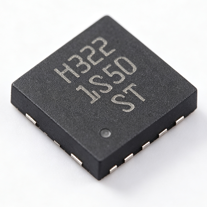
ST1S50PUR - 3A, 18V Synchronous Step-Down Converter | STMicroelectronics
The ST1S50PUR is a high-efficiency, synchronous step-down DC-DC converter from STMicroelectronics, designed to deliver up to 3A of continuous output current from an input voltage range of 4V to 18V. Housed in a compact DFN8 (3x3 mm) package, this device integrates both high-side and low-side power MOSFETs, eliminating the need for an external Schottky diode and simplifying PCB layout. The output voltage is adjustable from 0.8V to VIN, allowing flexibility for a wide range of applications. A synchronous buck converter is a type of DC-DC step-down regulator that uses two active switches (typically MOSFETs) instead of a diode for the low-side element, which significantly improves efficiency, especially at lower output voltages. This architecture is fundamental in power management ICs, where efficiency directly impacts battery life, thermal management, and system reliability. The ST1S50PUR belongs to the family of synchronous step-down converters, which are essential building blocks in modern electronic systems, from portable devices to industrial equipment. Key features of the ST1S50PUR include a fixed 1.5 MHz switching frequency, which allows the use of small, low-cost inductors and capacitors, reducing the overall solution footprint. The device offers a typical efficiency of 90% at 3A load, with a low quiescent current of 1.2 mA in light-load operation. It also features internal soft-start to limit inrush current, overcurrent protection, and thermal shutdown for robust operation. The DFN8 package has an exposed pad for enhanced thermal performance, with a thermal resistance of 40°C/W. The ST1S50PUR utilizes a current-mode control architecture, providing fast transient response and stable operation over a wide range of input and output voltages. The integrated MOSFETs have low RDS(on) (typically 120 mΩ high-side and 80 mΩ low-side), minimizing conduction losses. The device operates over a junction temperature range of -40°C to +150°C, making it suitable for demanding environments. Typical applications include point-of-load (POL) converters for FPGAs, DSPs, and microcontrollers, as well as power supplies for set-top boxes, networking equipment, and industrial control systems. The wide input voltage range also supports 12V and 24V bus systems, making it versatile for various power architectures. When designing with the ST1S50PUR, ensure proper input and output capacitor selection to maintain stability and minimize ripple. The exposed pad should be soldered to a large copper area for effective heat dissipation. The EN pin allows for power sequencing, and the soft-start feature prevents output overshoot during startup.
STNRG011ATR - Digital Power Controller for SMPS | STMicroelectronics
The STNRG011ATR is a digital power controller from STMicroelectronics designed for switched-mode power supplies (SMPS). It integrates a digital control core with a high-voltage startup cell, making it suitable for flyback, buck, and boost converter topologies. The device operates from an input voltage range of 8.5V to 23V and provides a gate drive output capable of sourcing 0.5A and sinking 0.8A. It is housed in a 16-pin SO-16 package, offering a compact solution for power supply designs. A digital power controller is a type of power management IC that uses digital signal processing to regulate output voltage and current, replacing traditional analog control loops. It sits within the hierarchy of power management ICs, which include linear regulators, switching regulators, and digital power controllers. Digital controllers offer advantages such as programmability, higher efficiency, and better transient response compared to analog counterparts. Key features of the STNRG011ATR include a programmable switching frequency up to 1 MHz, an integrated high-voltage startup cell that reduces standby power consumption, and a digital control loop that can be configured via an I2C interface. The device also includes protection features such as overcurrent protection, overvoltage protection, and thermal shutdown, ensuring reliable operation in demanding environments. The STNRG011ATR utilizes a digital control architecture with a dedicated state machine and a configurable PID compensator. This allows designers to optimize the control loop for specific power stage characteristics without changing external components. The integrated high-voltage startup cell enables fast startup and low standby power, making it ideal for applications requiring energy efficiency standards compliance. Typical applications include AC-DC adapters, USB Power Delivery (USB-PD) chargers, and industrial power supplies. The device's digital control capability allows for precise voltage and current regulation, which is essential for USB-PD applications that require multiple output voltage levels. Its wide input voltage range and high switching frequency support compact transformer designs, reducing overall solution size. When designing with the STNRG011ATR, ensure proper layout of the high-voltage startup cell and gate drive traces to minimize parasitic inductance. The I2C interface should be isolated from high-voltage areas to prevent noise coupling. Additionally, the thermal pad should be connected to a large copper area for effective heat dissipation.
STPM066S - 66V Step-Down DC-DC Converter | STMicroelectronics
The STPM066S is a high-voltage step-down DC-DC converter from STMicroelectronics, designed to deliver efficient power conversion in industrial and automotive applications. It operates from a wide input voltage range of 4.5V to 66V, making it suitable for 12V, 24V, and 48V bus systems. The device provides a continuous output current of up to 3A, with an adjustable output voltage down to 0.8V. Housed in a compact QFN-16 package (4x4 mm), the STPM066S integrates high-side and low-side MOSFETs, reducing external component count and simplifying PCB layout. A step-down DC-DC converter, also known as a buck converter, is a type of switching regulator that efficiently reduces a higher input voltage to a lower output voltage. Unlike linear regulators, which dissipate excess power as heat, buck converters use inductive energy storage and high-frequency switching to achieve efficiencies often exceeding 90%. This makes them essential in power management systems where thermal budget and battery life are critical. The STPM066S belongs to the broader category of power management ICs, specifically within DC-DC converters, and is a key building block in distributed power architectures. Key features of the STPM066S include a peak efficiency of 95%, a switching frequency adjustable from 200kHz to 2.2MHz, and a low quiescent current of 40uA in light-load mode. The device also offers a precision enable pin with hysteresis, soft-start to limit inrush current, and comprehensive protection features including overcurrent, overvoltage, and thermal shutdown. The integrated MOSFETs have low RDS(on) of 80mOhm (high-side) and 40mOhm (low-side), minimizing conduction losses. Technically, the STPM066S employs a current-mode control architecture, providing fast transient response and stable operation with a wide range of output capacitors. The adjustable switching frequency allows designers to optimize efficiency versus component size, while the external compensation pin offers flexibility in loop tuning. The device is available in a QFN-16 package with an exposed thermal pad, achieving a thermal resistance of 25°C/W, enabling reliable operation at high ambient temperatures. Typical applications include industrial power supplies, automotive infotainment systems, battery-powered equipment, and distributed power architectures in telecom and networking equipment. The wide input range and high efficiency make it ideal for pre-regulation in multi-rail systems, where it steps down a high-voltage bus to an intermediate rail for downstream LDOs or point-of-load converters. When designing with the STPM066S, ensure proper input and output capacitor selection to minimize voltage ripple and maintain stability. The bootstrap capacitor for the high-side driver must be placed close to the BST pin, and the feedback network should be routed away from the inductor to avoid noise coupling. Adequate copper pour on the thermal pad is essential for heat dissipation at high output currents.
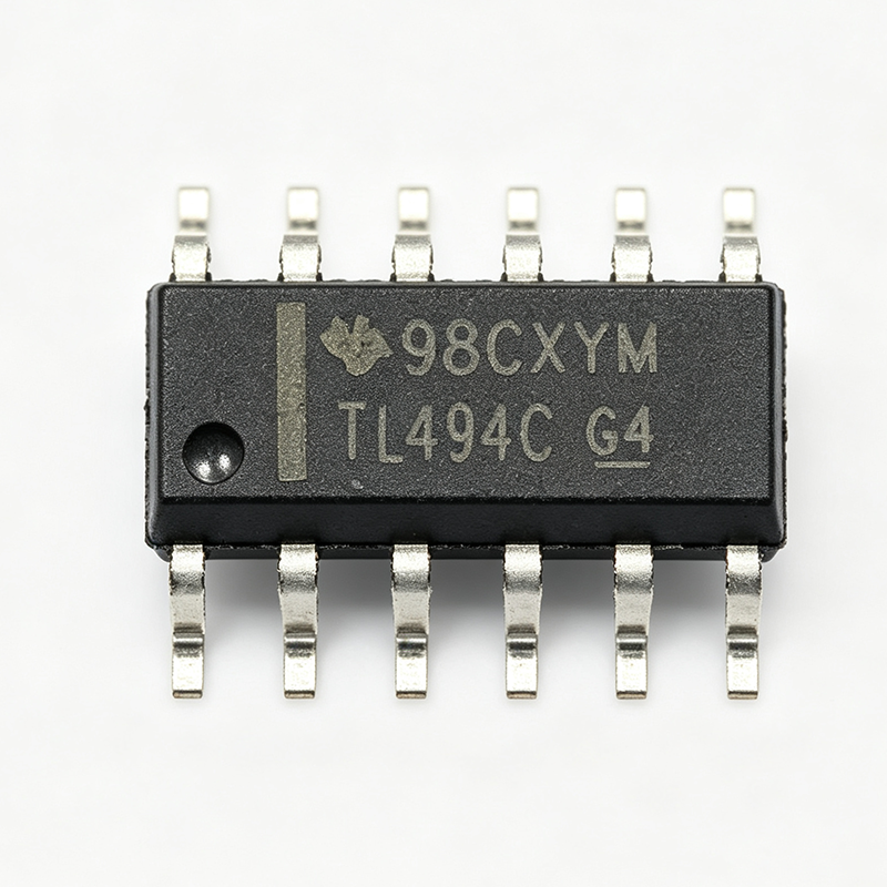
TL494CDT - PWM Controller IC | STMicroelectronics | SMPS
The TL494CDT is a fixed-frequency pulse-width modulation (PWM) control circuit from STMicroelectronics, designed primarily for switch-mode power supplies (SMPS). It integrates all the functions required for a single-ended or push-pull switching power supply, including an internal oscillator, error amplifiers, a 5V reference, and output control logic. The device operates from a supply voltage of 7V to 40V and is available in a 16-pin SOIC (SOP-16) package, making it suitable for compact power supply designs. A PWM controller is a specialized integrated circuit that generates a variable-duty-cycle square wave to regulate the output voltage of a switching power supply. It compares a feedback signal to a reference voltage and adjusts the duty cycle of the output transistors accordingly. The TL494 belongs to the family of voltage-mode PWM controllers, which are widely used in offline and DC-DC converters due to their simplicity and robustness. This category sits within the broader hierarchy of power management ICs, which also includes linear regulators, switching regulators, and battery management devices. Key features of the TL494CDT include a complete PWM power-control circuitry, an uncommitted output for single-ended or push-pull operation, an internal oscillator with a frequency range of 1kHz to 300kHz, and a 5V reference with 5% tolerance. It also provides an error amplifier with a common-mode voltage range of -0.3V to VCC-2V, a dead-time control comparator, and a standby current of typically 6mA. These features enable precise regulation and protection in various power conversion topologies. The TL494CDT uses a bipolar process technology, offering a proven and reliable architecture that has been in production for decades. It includes an internal 5V reference that can source up to 10mA for external use, and its output stage can sink or source up to 250mA. The device also features a shutdown control pin that can be used for overcurrent or overvoltage protection, and its dead-time control allows adjustment of the minimum off-time to prevent transformer saturation in push-pull designs. Typical applications include switch-mode power supplies for computers, telecom equipment, industrial systems, and battery chargers. The TL494CDT is also used in DC-DC converters, inverters, and motor control circuits. Its wide supply voltage range and flexible output configuration make it a versatile choice for both single-ended and push-pull topologies. When designing with the TL494CDT, it is important to properly set the oscillator frequency using external timing components (RT and CT) and to ensure adequate decoupling of the VCC pin. The dead-time control pin should be used to prevent shoot-through in push-pull stages, and the error amplifier compensation network must be designed for stable loop operation. This page synthesizes distributor pricing, drop-in alternatives, and practical design notes not found in the STMicroelectronics datasheet, providing a comprehensive resource for engineers selecting a PWM controller for their power supply design.
TNY277GN - 18.5W Offline Flyback Switcher | Power Integrations
The Power Integrations TNY277GN is an energy-efficient, off-line switcher IC from the TinySwitch-III family, designed for flyback power supplies. It integrates a 700 V power MOSFET, oscillator, high-voltage switched current source, user-selectable current limit, and thermal shutdown circuitry in a compact SMD-8C package. The device operates at a fixed switching frequency of 132 kHz and delivers up to 18.5 W output power from a universal input range of 85 VAC to 265 VAC, or 23.5 W from 230 VAC. Its simple ON/OFF control scheme eliminates the need for loop compensation, reducing external component count and system cost. An off-line switcher is a power management IC that converts AC mains voltage directly to a regulated DC output, typically using a flyback or buck topology. It integrates the power switch (MOSFET) and control circuitry into a single package, simplifying the design of AC-DC power supplies. The TinySwitch-III family is a specific series of off-line switchers from Power Integrations, known for their high efficiency, low standby power, and ease of use. These ICs are widely used in chargers, adapters, and auxiliary power supplies. Key features of the TNY277GN include a 700 V MOSFET for wide input voltage handling, a user-selectable current limit for design flexibility, and built-in thermal shutdown for protection. The device also features frequency jittering to reduce EMI, making it easier to meet electromagnetic compatibility standards. Its ON/OFF control scheme provides excellent load regulation without the need for an optocoupler in many designs, simplifying the feedback loop. Technically, the TNY277GN uses a current-mode control architecture with a high-voltage switched current source for startup, eliminating the need for a separate startup resistor. The device's EcoSmart technology ensures low standby power consumption, making it suitable for energy-efficient applications. The SMD-8C package is designed for surface-mount assembly, offering a compact footprint for space-constrained designs. Typical applications include AC-DC adapters, battery chargers, standby power supplies for TVs and monitors, and auxiliary power supplies for appliances. The TNY277GN is particularly well-suited for applications requiring high efficiency and low standby power, such as Energy Star compliant products. When designing with the TNY277GN, ensure proper transformer design and adequate PCB layout to minimize leakage inductance and EMI. The device's thermal shutdown feature protects against overtemperature conditions, but proper heat sinking through the PCB copper area is recommended for reliable operation at full load.
TNY277GN-TL - 18.5W Offline Flyback Switcher | Power Integrations
The Power Integrations TNY277GN-TL is an offline flyback switcher IC from the TinySwitch-III family, integrating a 700 V power MOSFET, oscillator, high-voltage switched current source, current limit (user selectable), and thermal shutdown circuitry in a compact SMD-8C (7-lead) package. It delivers up to 18.5 W output power from a universal input range of 85-265 VAC, and 23.5 W at 230 VAC, making it ideal for low-power AC-DC power supplies. TinySwitch-III is a family of energy-efficient, low-power offline switchers that use a simple ON/OFF control scheme, eliminating the need for loop compensation. This simplifies design and reduces component count, lowering system cost. The IC operates at a fixed frequency of 132 kHz with frequency jittering to reduce EMI, and includes a user-selectable current limit to optimize efficiency and power delivery. Key features include a 700 V power MOSFET, integrated oscillator, high-voltage switched current source for fast startup, current limit selection, and comprehensive protection features such as over-temperature protection, overvoltage protection, and line undervoltage detection. The EN/UV pin senses line undervoltage through an external resistor, and if absent, disables the line undervoltage function. The device also features leading edge blanking to prevent false triggering. The TNY277GN-TL is designed for high efficiency and low standby power, meeting energy efficiency standards. Its integrated 700 V MOSFET allows direct connection to the rectified AC line, simplifying the primary-side circuit. The SMD-8C package with gull-wing leads is suitable for automated assembly and provides good thermal performance. Typical applications include auxiliary power supplies for appliances, standby power for TVs and monitors, AC-DC adapters, and industrial control power supplies. The wide input voltage range and robust protection make it suitable for global applications. When designing with this device, ensure proper PCB layout with adequate creepage distances for high-voltage isolation, and follow the recommended transformer design in the datasheet to achieve optimal performance and EMI compliance.

TNY277PG - 23.5W Offline Switcher IC | Power Integrations
The Power Integrations TNY277PG is an energy-efficient, off-line switcher IC from the TinySwitch-III family, designed for flyback power supplies up to 23.5 W at 230 VAC or 18 W at 85-265 VAC. It integrates a 700 V power MOSFET, oscillator, high-voltage switched current source, user-selectable current limit, and thermal shutdown circuitry in an 8-pin PDIP-C package (7 leads). The device uses a simple ON/OFF control scheme that eliminates the need for loop compensation, reducing external component count and system cost. An off-line switcher is a power management IC that converts AC mains voltage directly to a regulated DC output, typically using a flyback or buck topology. It combines a high-voltage power switch, control logic, and protection features in a single package, simplifying the design of AC-DC power supplies. The TinySwitch-III family is part of the broader class of switched-mode power supply (SMPS) controllers, which are essential in applications ranging from chargers to industrial power supplies. Key features of the TNY277PG include a 700 V MOSFET for wide input voltage range, a 132 kHz switching frequency for compact magnetics, and selectable current limit for design flexibility. The ON/OFF control scheme provides excellent efficiency across load conditions, and the device includes auto-restart protection for output short-circuit and open-loop faults. The 8-PDIP-C package (7 leads) is through-hole mounted, making it easy to prototype and manufacture. Technically, the TNY277PG integrates the high-voltage power switch and control circuitry on a single die, reducing parasitic inductance and improving reliability. The high-voltage switched current source enables fast startup and low standby power, meeting energy-efficiency standards. The device also features a frequency jittering function to reduce EMI, simplifying filter design. Typical applications include AC-DC adapters, chargers, standby power supplies, and auxiliary power supplies for appliances and industrial equipment. The wide input range and high efficiency make it suitable for global markets. When designing with the TNY277PG, ensure proper heat sinking for the PDIP package at high output power, and follow the recommended PCB layout for the primary-side circuitry to minimize EMI and ensure stable operation.
TNY277PN - 18.5W Flyback Switcher IC | Power Integrations
The Power Integrations TNY277PN is an energy-efficient offline switcher IC from the TinySwitch-III family. It integrates a 700 V power MOSFET, a 132 kHz oscillator, a high-voltage switched current source, user-selectable current limit, and thermal shutdown circuitry into a through-hole 8-PDIP-C package. Under an 85-265 VAC universal input range, the device delivers up to 18.5 W output; at a fixed 230 VAC input it supports up to 23.5 W. These ratings make it suitable for open-frame adapter and auxiliary supply designs that require a simple two-terminal flyback converter stage. An offline switcher is a power-management integrated circuit that accepts rectified AC line voltage and performs high-frequency switching to provide one or more isolated DC outputs through a flyback transformer. The TinySwitch-III family is a subcategory of AC-DC converters, which sit above linear regulators and standard DC-DC converters in the power conversion hierarchy. By integrating the power MOSFET and controller on one chip, offline switcher ICs reduce BOM count, simplify PCB layout, and improve reliability compared to discrete controller-plus-MOSFET implementations. Key features of the TNY277PN include the built-in 700 V power MOSFET, which provides wide margin for line-voltage spikes and improves surge robustness. The integrated high-voltage switched current source accelerates startup and reduces no-load input power. The user-selectable current limit lets designers optimize transformer size for the target power level, while the 132 kHz switching frequency balances transformer size against switching losses. Thermal shutdown protects the IC against secondary-side overload or fault conditions. In operation, the IC uses a simple ON/OFF control scheme that requires no external loop compensation. The internal oscillator controls the power MOSFET duty cycle; when output feedback demands energy, the MOSFET switches, then enters a low-power state. This burst-mode operation at light load reduces standby losses and is especially useful for Energy Star-compliant adapters. The through-hole 8-pin DIP package simplifies assembly and helps transfer heat to PCB copper in moderate-power designs. Typical applications include AC/DC adapters and battery chargers, standby and auxiliary power supplies for appliances, LED drivers, industrial control supplies, and IoT smart-home power modules. The flyback topology pairs with inexpensive transformers and standard optocoupler/TL431 feedback networks. When designing with TNY277PN, pay attention to drain snubber selection, transformer leakage inductance, and BP/M pin decoupling. A well-laid-out PCB with tight loop areas is critical for meeting conducted EMI limits.
TPS53315 - 12A D-CAP Buck Regulator | Texas Instruments
The Texas Instruments TPS53315 is a D-CAP mode, 12-A synchronous step-down (buck) regulator with integrated MOSFETs, offered in a 5 mm x 7 mm 40-pin VQFN (RGF) package with exposed thermal pad. It supports a supply voltage of 4.5 V to 25 V, conversion input of 3 V to 15 V, and adjustable output from 0.6 V to 5.5 V, targeting ease of use, low external component count, and compact point-of-load power systems. A buck converter is a type of switching DC-DC regulator that efficiently reduces a higher voltage to a lower one. The TPS53315 belongs to the synchronous buck family, using both high-side and low-side MOSFETs for high efficiency, and sits within the broader power management IC hierarchy for point-of-load conversion. Key features include 12-A continuous output current, integrated 19-mOhm high-side and 7-mOhm low-side MOSFETs that minimize conduction losses, an accurate 1% 0.6-V reference, and an integrated boost switch that removes the external bootstrap diode. D-CAP control delivers fast load transient response without external compensation and is stable with ceramic output capacitors. Technically, the proprietary D-CAP architecture combines constant on-time control with adaptive on-time, enabling low output ripple and fast transient behavior. Overcurrent protection, thermal shutdown, and a power-good indicator improve system robustness. The exposed-pad VQFN package provides thermal performance around 25 C/W junction-to-ambient per internal data. Typical applications include point-of-load power for FPGAs, ASICs, and DSPs, as well as server, storage, networking, industrial, and telecom power rails where high efficiency and small size matter. Design tip: use at least 2 x 22 uF ceramic output capacitance for stability and pay careful attention to PCB layout of the power stage and exposed pad for thermal dissipation.
TPS53315 - 12A D-CAP Sync Buck Regulator | Texas Instruments
The Texas Instruments TPS53315 is a D-CAP mode, 12-A synchronous step-down (buck) switching regulator with integrated MOSFETs, housed in a 5 mm x 7 mm 40-pin VQFN package with exposed pad. It is designed for ease of use, low external component count, and compact power systems, with a 0.6 V to 5.5 V adjustable output and single-rail input support. A DC-DC switching regulator (specifically a synchronous buck converter) steps a higher input voltage down to a regulated lower output voltage using integrated power MOSFETs and an external inductor. The D-CAP control topology uses an internally compensated, constant-on-time architecture that eliminates complex external compensation networks and delivers excellent load transient response, placing the TPS53315 high in the power management IC hierarchy: buck converter -> switching regulator -> DC-DC converter -> PMIC. Key features include up to 12 A of continuous output current, one 19-mOhm high-side and one 7-mOhm low-side integrated MOSFET, an accurate 1% 0.6-V voltage reference, and an integrated boost switch for the high-side gate drive. The conversion input voltage range spans 3 V to 15 V, while the supply voltage (VDD) range is 4.5 V to 25 V, allowing a single rail to power both control and conversion stages in many systems. Architecturally, the D-CAP constant-on-time scheme provides near-constant switching frequency with fast transient response and low output ripple, requiring only a small set of external components: input/output capacitors, an inductor, and a feedback divider. This minimizes BOM cost and PCB area compared to traditional voltage-mode controllers with external FETs. Typical applications include point-of-load power for DSPs, FPGAs, and ASICs in networking, telecom, industrial, and computing equipment, where multi-amp core or I/O rails must be generated efficiently from a 5 V or 12 V intermediate bus. It also suits distributed power architectures and dense server memory rails. Design consideration: with 12 A output in a compact VQFN-40 package, PCB thermal design is critical - use generous copper pour on the exposed pad and follow the TI datasheet layout guidelines for the power stage loop to minimize EMI and voltage spikes.
TPS53355DQPR - 30A Sync Buck Converter 1.5-15V | TI
The Texas Instruments TPS53355DQPR is a 30-A D-CAP mode synchronous step-down (buck) converter with integrated 5-mOhm high-side and 2-mOhm low-side MOSFETs, supporting a 1.5-V to 15-V input range and a 0.6-V to 5.5-V adjustable output in a 6-mm x 5-mm, 22-pin QFN (DQP) package. A synchronous buck converter is a DC-DC switching regulator that uses two internally integrated MOSFETs and an external inductor to step a higher input voltage down to a lower, tightly regulated output voltage. Buck regulators form the core of modern point-of-load power management hierarchies, converting intermediate distribution rails (such as 12 V) into the low voltages required by processors, FPGAs, and memory, with far higher efficiency than linear regulators. Key features include the D-CAP control topology, which requires no external compensation network and delivers excellent load transient response, plus TI eco-mode technology that reduces switching frequency at light load to maintain high efficiency across the full load range. The internal 5-mOhm/2-mOhm MOSFET pair minimizes conduction losses at full 30-A output, while the accurate 1% 0.6-V internal reference supports low-voltage core rails. An integrated boost switch eliminates an external bootstrap diode. Technically, the device supports adjustable switching frequency (250 kHz to 1 MHz), adjustable current limit with thermal shutdown protection, and flexible soft-start control. The wide 1.5-V to 15-V conversion input allows direct operation from 12-V intermediate bus rails as well as 5-V and lower rails. Typical applications include server and network processor core power, point-of-load supplies for FPGAs, ASICs, and DDR memory, telecom and datacenter power stages, and distributed power systems where a compact 30-A stage with minimal external components is required. Design consideration: at 30-A output the power stage dissipation is dominated by conduction losses, so a solid PCB thermal layout with generous copper pour on the exposed thermal pad is essential for reliable continuous operation. This page synthesizes distributor availability data, drop-in alternatives, and practical design notes not found in the manufacturer datasheet alone.
TPS53511RGTR - 1.5A Sync Buck Regulator 4.5-18V | TI
The Texas Instruments TPS53511RGTR is a 1.5 A adaptive on-time D-CAP2 mode synchronous step-down (buck) converter with integrated switching MOSFETs, accepting a 4.5 V to 18 V input and delivering an adjustable output down to 0.76 V, housed in a 16-pin VQFN (RGT) package with exposed pad rated from -40C to +85C. A synchronous buck converter is a DC-DC switching regulator that steps a higher input voltage down to a lower output voltage using two internal MOSFETs (high-side and low-side) alternating between input and ground. Compared with a linear regulator, a buck converter achieves high efficiency through switched-mode power conversion, and it sits within the broader hierarchy of power management ICs (PMICs), under voltage regulators and DC-DC converters. Synchronous rectification replaces the external freewheeling diode with a low-side MOSFET, reducing conduction losses. Key features of the TPS53511 include the D-CAP2 control topology, which provides fast transient response with no external compensation components, making the design cost-effective with a low external component count; integrated MOSFETs that eliminate the need for external power switches; and low standby current suited to always-on points-of-load. The adaptive on-time (AOT) architecture dynamically adjusts the switching pulse width against input and output conditions to maintain regulation across load ranges. Technically, D-CAP2 mode combines an internal ripple-generation network with an adaptive on-time scheme, enabling stable operation with small ceramic output capacitors and supporting a wide duty-cycle range for computing power systems. The exposed-pad VQFN-16 (RGT) package provides low thermal impedance to the PCB, and the 4.5 V to 18 V input range covers 5 V, 12 V intermediate bus rails and most AC-DC adapter outputs. Typical applications include points-of-load (POL) regulation in computing power systems, network and communication equipment, consumer electronics, and industrial subsystems requiring a compact, low-component-count 1.5 A buck stage. Cost sensitivity and fast load transients make it a strong fit for memory, SoC core and I/O rails. For design, choose an output capacitor with low ESR to support the D-CAP2 ripple-injection scheme, and verify minimum on-time limits when converting 18 V down to very low outputs. Keep the SW, BOOT and VIN loops tight on the PCB layout. This page synthesizes distributor pricing (as of 2026-09-10), pin-compatible drop-in alternatives including the pin-for-pin TPS54326, and practical design notes not consolidated in the manufacturer datasheet.
TPS53513RVER - 8A, 18V Sync Buck Converter | Texas Instruments
The Texas Instruments TPS53513RVER is an 8 A synchronous SWIFT step-down (buck) converter with a 1.5 V to 18 V input range, adjustable 0.6 V to 5.5 V output, and an adaptive on-time D-CAP3 control mode, housed in a 28-pin VQFN (RVE) package with exposed pad. A synchronous buck converter is a type of DC-DC switching regulator that steps a higher input voltage down to a lower output voltage using two integrated MOSFETs (a high-side and a low-side switch) instead of an external Schottky diode. Within the power management IC hierarchy, it belongs to the family of switching voltage regulators, which achieve far higher efficiency than linear regulators, making them the standard choice for point-of-load power conversion in digital systems. Key features of the TPS53513 include integrated 13.8-mOhm high-side and 5.9-mOhm low-side MOSFETs delivering 8 A of continuous output current, a precision 600 mV reference with 0.5% tolerance, support for all-ceramic output capacitors, and an integrated boost switch that eliminates one more external component. Technically, the D-CAP3 control topology is an adaptive on-time architecture that provides fast transient response to load steps without complex loop compensation, allowing a very low external-component count. Because switching frequency adapts to input and output conditions, the converter maintains good efficiency across light and heavy loads while supporting high step-down ratios from 18 V rails. Typical applications include powering FPGAs, ASICs, microprocessors, and DSP cores in networking, telecom, industrial, and server equipment, where a compact 8 A point-of-load solution from a 12 V intermediate bus is required. For design, note the device is specified from -40C to +85C ambient; at 8 A loads with 18 V input, thermal design of the exposed-pad PCB land pattern is critical, and all-ceramic output capacitance must be verified against D-CAP3 stability requirements. This page synthesizes distributor pricing, drop-in alternatives, comparison tables, and practical design notes not found in the manufacturer datasheet alone.
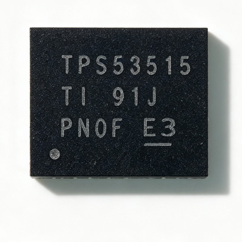
TPS53515RVER - 12A Sync Buck Converter 18V In | Texas Instruments
The Texas Instruments TPS53515RVER is a 12 A synchronous SWIFT step-down buck converter with an adaptive on-time D-CAP3 control mode, supporting a 1.5 V to 18 V input range (4.5 V to 25 V bias) and an adjustable 0.6 V to 5.5 V output, housed in a 28-pin VQFN exposed-pad package. It integrates 13.8 mOhm high-side and 5.9 mOhm low-side MOSFETs plus a boost switch for minimal external component count. A buck (step-down) converter is a switching voltage regulator that converts a higher input voltage to a lower regulated output using an inductor, switches, and output capacitors. Within the power-management hierarchy, the TPS53515 sits at the power-management IC level as a fully integrated point-of-load (POL) switching regulator, combining controller and power stage in one package. Key features include 12 A continuous output current with high-performance integrated MOSFETs, a 600 mV voltage reference with +/-0.5% tolerance for precise output settings, and D-CAP3 control delivering fast load-step transient response. The device supports all-ceramic output capacitors, eliminating electrolytic capacitors and improving reliability and board height. Technically, the adaptive on-time D-CAP3 architecture varies the on-time with input and output voltage to maintain near-constant switching frequency, providing ease of use and ultra-fast transient response without complex loop compensation. The integrated boost switch drives the high-side MOSFET gate without an external bootstrap diode, and the low on-resistance MOSFETs yield high conversion efficiency at heavy loads. TI's inductor-on-top reference design achieves greater than 87% efficiency with about 2.6 W power loss at 12 A load and 12 mV output ripple using only 10x22 uF ceramic output capacitors. Typical applications include point-of-load supplies for ASICs, DSPs, and FPGAs, network and telecom infrastructure cards, and industrial DC-DC power stages where a compact 12 A solution with minimal external parts is needed. When designing, ensure the bias pin is supplied within its 4.5 V to 25 V range for reliable gate drive, and select the inductor based on the recommended values in the datasheet for stability across the 0.6 V to 5.5 V output range. This page synthesizes distributor pricing, drop-in alternatives, comparison data, and practical design notes not found in the manufacturer datasheet.