DC-DC Converters
Products (207)
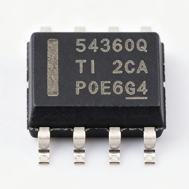
TPS54360QDDARQ1 - 60V 3.5A Buck Converter | Texas Instruments
The Texas Instruments TPS54360QDDARQ1 is an AEC-Q100 qualified 4.5V to 60V input, 3.5A step-down DC-DC converter with an integrated high-side MOSFET, supplied in an 8-pin SO-8 PowerPAD (DDA) package. The regulated output is adjustable from 0.8V using a resistor divider, making this a single-output buck switching regulator for automotive and industrial power supplies. A buck (step-down) converter is a switching voltage regulator that converts a higher input voltage to a lower regulated output using an internal power switch, external inductor, and output capacitor. Within the power management hierarchy, this device sits in the DC-DC converter family, part of the broader voltage regulator and power management IC (PMIC) domain, optimized for wide-input point-of-load conversion directly from automotive battery rails. Key features include a 60V maximum input with 65V transient survivability per ISO 7637 load-dump testing, 3.5A continuous output current, TI Eco-mode pulse-skip operation for high light-load efficiency, and current-mode control for simple external compensation and flexible component selection. The automotive Q1 qualification and -40C to +125C ambient range enable deployment in harsh vehicle environments. Architecturally, the device uses peak current-mode control with an integrated 60V power MOSFET, reducing external component count versus a controller-plus-discrete-FET solution. The low-ripple pulse-skip Eco-mode reduces switching losses at light loads, while the internal bootstrap and soft-start functions simplify startup design. The SO-8 PowerPAD exposed pad provides a low thermal resistance path for heat dissipation. Typical applications include automotive infotainment and cluster power rails, 12V/24V industrial bus point-of-load conversion, USB and display bias supplies, and general-purpose wide-input regulation from 24V industrial systems. Design consideration: at 60V input the converter operates at high switching-step ratios; ensure the external inductor saturation current exceeds the 3.5A peak limit and follow the TI datasheet layout guidelines, placing the input decoupling capacitor very close to VIN and GND pins.
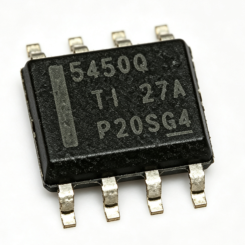
TPS5450QDDARQ1 - 5A 36V Automotive Buck Converter | TI
The Texas Instruments TPS5450QDDARQ1 is an AEC-Q100 qualified 5A step-down (buck) switching regulator that accepts a wide 5.5V to 36V input and delivers an adjustable output from 1.221V to 31V, housed in a thermally enhanced 8-pin HSOIC (DDA) PowerPAD package. It supports 5A continuous and 6A peak output current at a fixed 500 kHz switching frequency. A DC-DC buck converter is a switching voltage regulator that steps a higher input voltage down to a lower regulated output using PWM switching, achieving far higher efficiency than linear regulators. Within the power management IC hierarchy, the TPS5450-Q1 is a non-synchronous, internally compensated voltage-mode SWIFT converter IC. Key features include a 500 kHz fixed switching frequency, voltage-mode PWM control, an active-high enable (ENA) pin that reduces shutdown supply current to 18 uA, and full protection: cycle-by-cycle overcurrent limiting, overvoltage protection, and thermal shutdown. Internal feedback-loop compensation dramatically reduces external component count and design complexity. Technically, the integrated high-side N-channel MOSFET and internal compensation allow a minimal external BOM - only an inductor, catch diode, feedback divider, and small input/output capacitors. The PowerPAD (DDA) package provides a low thermal impedance path to the PCB, and the 500 kHz switching frequency permits a compact inductor while keeping switching losses manageable across the 36V automotive input range, including load-dump-tolerant designs. Typical applications include automotive infotainment and cluster 5V rails, ADAS and body-control module 12V-to-5V point-of-load conversion, and industrial 24V-bus step-down supplies where wide input headroom and 5A capability are required. Design consideration: because the converter is non-synchronous, select a Schottky catch diode rated for the full output current with low forward drop, placed close to the PH pin; the exposed PowerPAD must be soldered to a solid ground copper pour for thermal performance. This page synthesizes distributor pricing, same-brand drop-in alternatives, and practical design notes not found in the manufacturer datasheet, with prices as of 2026-09-01.
TPS54620 - 6A Synchronous Buck Converter | Texas Instruments
The Texas Instruments TPS54620 is a highly-integrated, synchronous, step-down DC-DC converter that converts a higher DC input voltage to a lower DC output voltage with a maximum output current of 6 A. It operates from a 4.5-V to 17-V input supply and provides an adjustable output voltage down to 0.8 V with ±1% reference accuracy. The device is available in a thermally enhanced 3.50 mm × 3.50 mm QFN package (RGY), which is optimized for small designs through high efficiency and integration of the high-side and low-side MOSFETs. A synchronous buck converter is a type of DC-DC switching regulator that steps down voltage with high efficiency by using two transistors (high-side and low-side) that switch alternately, minimizing conduction losses compared to asynchronous designs. It belongs to the broader category of voltage regulators, which are essential in power management ICs for converting and stabilizing supply voltages in electronic systems. The TPS54620 integrates both MOSFETs, reducing external component count and board space. Key features include integrated 26 mΩ and 19 mΩ MOSFETs, a split power rail allowing 1.6 V to 17 V on PVIN, a switching frequency range of 200 kHz to 1.6 MHz, synchronization to an external clock, and a low 2-μA shutdown quiescent current. These features enable high efficiency across a wide load range and flexible design for noise-sensitive applications. Technically, the TPS54620 uses a current-mode control architecture with pulse-by-pulse current protection, ensuring robust operation under overload conditions. The 0.8-V reference with ±1% accuracy over temperature provides precise output regulation. The device also includes thermal shutdown and overcurrent protection, enhancing reliability in demanding environments. Typical applications include industrial power supplies, automotive infotainment, telecom equipment, and point-of-load converters for FPGAs and DSPs. Its wide input range and high output current make it suitable for 12-V bus systems and battery-powered devices. When designing with the TPS54620, ensure proper input and output capacitor selection to minimize ripple and maintain stability. The switching frequency can be synchronized to an external clock to avoid beat frequencies in multi-rail systems. Thermal management is critical; the QFN package's exposed pad must be soldered to a sufficient copper area for heat dissipation.
TPS548B28 - 20A, 16V Synchronous Buck Converter | TI
The Texas Instruments TPS548B28 is a 2.7-V to 16-V input, 20-A synchronous buck converter with differential remote sense, integrated MOSFETs, a 3-V internal LDO, and hiccup current limit, supplied in a 21-pin VQFN (RWW) package. It delivers an adjustable output from 0.6 V to 5.5 V with a ±1%, 0.6-V reference accurate over the full operating junction temperature range. A synchronous buck converter (also called a step-down switching regulator) is a DC-DC power management IC that uses integrated high-side and low-side MOSFETs plus an external inductor to convert a higher input voltage to a lower output voltage with high efficiency. Within the power-management hierarchy, the TPS548B28 sits at the point-of-load (POL) regulator level of server, storage, and computing power trees. Key features include 4-V to 16-V input range up to 20 A without external bias (2.7-V to 16-V with external bias from 3.13 V to 3.6 V), integrated 7.7-mΩ high-side and 2.4-mΩ low-side MOSFETs supporting 20-A continuous output, Skip-mode or FCCM operation for light-load efficiency, and programmable soft start. Differential remote sense improves output accuracy at the load point in dense boards. Technically, the integrated power stage minimizes external component count, making the part well-suited to space-constrained datacenter applications. Fast load-transient response, accurate load and line regulation, and hiccup-mode overcurrent protection improve system robustness; the internal 3-V LDO simplifies bias by allowing operation directly from the input rail. Typical applications include server and storage point-of-load rails, networking line cards, and computing ASIC/FPGA/DSP power supplies requiring 20 A or less at 0.6-V to 5.5-V outputs. Design tip: use the TPS548B28EVM-023 evaluation board as a layout reference, keep the SW loop compact, and note the device is not intended for paralleled outputs - use TPS53355 or LM27403 for parallel designs.
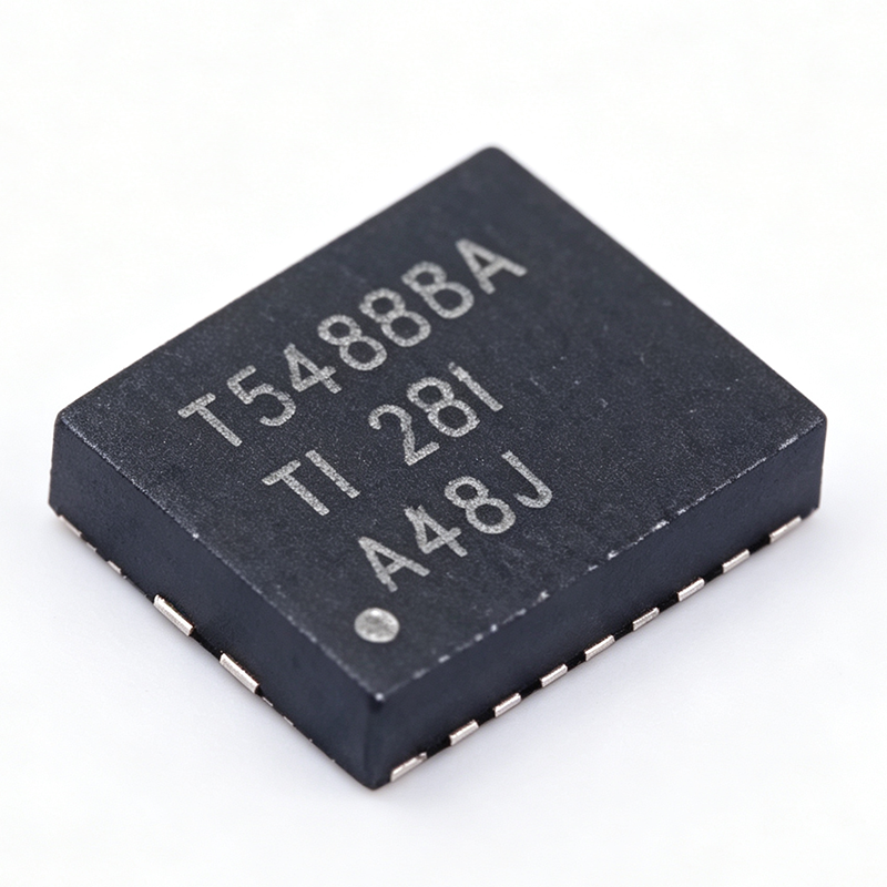
TPS548B28RWWR - 20A 16V Sync Buck Converter | TI | Datacenter
The Texas Instruments TPS548B28 is a 2.7V to 16V input, 20A synchronous buck converter with differential remote sense, integrated MOSFETs, and a 3V internal LDO, supplied in a 21-pin PowerVFQFN (RWW) package. With an accurate ±1% 0.6V reference over the full operating junction temperature range, it delivers precise point-of-load regulation for high-current computing loads. A synchronous buck converter is a DC-DC switching regulator that steps a higher input voltage down to a lower output voltage using two integrated switches (high-side and low-side MOSFETs) plus an external inductor. Within the power management hierarchy, the TPS548B28 belongs to the switching regulator family, positioned as a single-channel point-of-load (POL) solution between simple low-current bucks and multi-phase controllers. Key features include a 4V to 16V input range supporting 20A continuous output without external bias, extended 2.7V operation with a 3.13V to 3.6V external bias, an output voltage range of 0.6V to 5.5V, and integrated 7.7-mΩ high-side and 2.4-mΩ low-side MOSFETs. The device offers fast load-transient response, accurate load and line regulation, Skip-mode or forced-CCM (FCCM) operation for light-load efficiency trade-offs, programmable soft start, and hiccup current limit for fault robustness. The D-CAP3-style control architecture enables a small external component count and fast transient response with low output capacitance, well suited to space-constrained boards. The internal 3V LDO can be overridden by an external bias rail to improve efficiency at lower input voltages. Differential remote sense compensates for PCB IR drop, maintaining ±1% regulation at the load point. Typical applications include server and storage point-of-load rails (DSP, FPGA, ASIC, and processor cores), datacenter and networking card power, and general industrial 20A-class low-voltage supplies. Reference design support is available via the TPS548B28EVM-023 evaluation module. Design consideration: at 20A loads, minimize the SW-node copper area and optimize the input capacitor loop to control EMI; verify thermal performance since total MOSFET conduction plus switching losses concentrate in the small QFN footprint.
TPS55165-Q1 - 36V 1A Buck-Boost Regulator | Texas Instruments
The Texas Instruments TPS55165QPWPRQ1 is an AEC-Q100 qualified, 36-V rated, 1-A output, 2-MHz single-inductor synchronous buck-boost voltage regulator that produces a fixed 5 V or 12 V output in a 20-pin PowerTSSOP (PWP) package. It is designed for automotive and industrial power systems where the input can be above, below, or equal to the output voltage. A buck-boost converter is a non-isolated DC-DC switching regulator within the broader voltage regulator and power management IC hierarchy that maintains a regulated output even when the input voltage crosses the output level. The TPS55165-Q1 uses four integrated switches and a single inductor, with TI's buck-boost overlap control ensuring automatic, seamless transition between step-down and step-up modes with optimal efficiency and minimal output ripple. Key features include a wide input voltage range up to 36 V, fixed 5 V or 12 V output selection, 2 MHz switching frequency that allows small inductors and fast transient response, synchronous rectification for high efficiency, and a power-good (PG) pin for rail monitoring. The Q1 designation confirms AEC-Q100 qualification for automotive applications. The same TPS5516x-Q1 family includes the TPS55160-Q1 and TPS55162-Q1, which offer configurable outputs of 5.7 V to 9 V via an external resistive divider, sharing the same package and pinout. Typical applications include automotive start-stop and cold-crank power conditioning, 12 V battery-rail stabilization, automotive infotainment and cluster displays, and renewable-energy harvesting modules such as the RAK WisBlock RAK19004 green power module, which uses the TPS55165-Q1 to convert solar or hydro power to a fixed 5 V rail. Design consideration: because it is a boost-type topology, ensure the input pin cannot be shorted to output before the converter starts; TI datasheet SLVSDY1 provides layout and external component guidance.

TPS561201DDCR - 17V 1A Synchronous Buck | Texas Instruments
The TPS561201DDCR is a 1A synchronous step-down (buck) converter from Texas Instruments, operating from a 4.5V to 17V input. It provides an adjustable output from 0.76V to 7V, switching at a fixed 580kHz. Housed in a 6-pin SOT-23-THN (DDC) package measuring 1.6mm x 2.9mm, it is designed for space-constrained, cost-sensitive point-of-load applications. A synchronous step-down voltage regulator is a DC-DC converter that uses two actively controlled switches (high-side and low-side MOSFETs) to efficiently lower a higher DC voltage to a lower regulated voltage. Unlike asynchronous regulators, the low-side switch replaces the freewheeling Schottky diode, reducing conduction losses and improving efficiency. This converter belongs to the broader family of switch-mode power supplies (SMPS) within power management ICs. Key features include D-CAP2 control, which simplifies loop compensation by requiring only a low-ESR ceramic output capacitor for stable operation. The device has an enable pin for power sequencing, fixed soft start to limit inrush current, and pulse skip mode for light-load efficiency. The quiescent current is only 0.4mA typical, contributing to high light-load efficiency. The device integrates a synchronous rectifier, eliminating an external Schottky diode and reducing board area. Internal cycle-by-cycle current limit and thermal shutdown protect the IC. The fixed 580kHz switching frequency offers a balanced trade-off between efficiency and component size, enabling small inductors and output capacitors. D-CAP2 mode also provides fast transient response, making it suitable for processors and FPGAs with dynamic loads. Typical applications include set-top boxes, smart TVs, networking equipment, industrial control systems, white goods, and battery-powered devices. On a 12V industrial bus, it can produce clean 3.3V or 5V rails for MCUs and I/O. The enable pin supports power sequencing in multi-rail systems. When designing with this part, use approximately 10uF input and 22uF output capacitance placed close to the device. Because the SOT-23 package is small, pay careful attention to thermal dissipation; at higher power loss a larger copper area is necessary to keep the junction temperature within the -40C to +125C range.
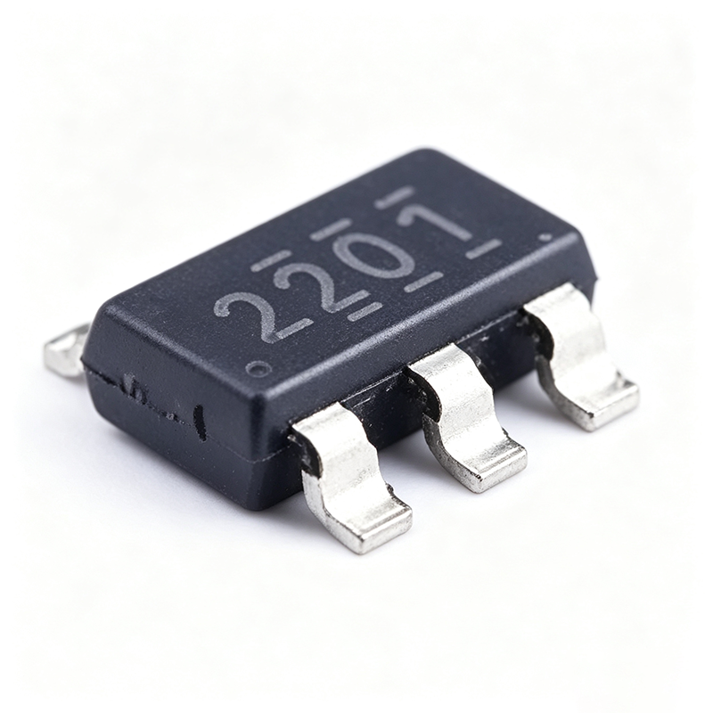
TPS562201DDCT - 2A 17V Sync Buck Converter | Texas Instruments
The Texas Instruments TPS562201DDCT is a 2A synchronous step-down (buck) converter in a compact 6-pin SOT-23-Thin (DDC) package, operating from a 4.5V to 17V input and producing an adjustable output from 0.768V to 7V at a fixed 580 kHz switching frequency. It integrates both high-side and low-side MOSFETs, eliminating the need for an external Schottky diode. A DC-DC switching regulator converts a higher input voltage to a lower regulated output using power switches and an inductor, offering far higher efficiency than a linear regulator. Within the power management IC hierarchy, the TPS562201 belongs to the synchronous buck converter family and is part of TI's D-CAP2 controller portfolio for point-of-load (POL) rails. Key features include the D-CAP2 control architecture, which provides fast transient response and supports both low-ESR and ceramic output capacitors with internal compensation, so no complex loop design is needed. Eco-mode pulse-skip operation maintains high efficiency at light loads by reducing switching frequency, while the 580 kHz fixed frequency allows small inductors and capacitors. Technically, the internally compensated adaptive on-time loop reacts within microseconds to load steps, making the part well suited to processor core and I/O rails. Internal soft-start limits inrush current, and the device is specified over a -40C to +125C junction temperature range in the 2.9 mm x 1.6 mm SOT-23-Thin package. Typical applications include 5V and 12V distributed-power point-of-load regulation, networking and telecom equipment, industrial automation systems, set-top boxes, and digital TV power supplies, where the 17V maximum input accepts 12V rails with headroom. Design consideration: keep the output voltage within the 0.768V to 7V range and use the datasheet-recommended ceramic output capacitance for D-CAP2 stability; place input decoupling capacitors as close as possible to the VIN and GND pins. This page synthesizes distributor pricing, drop-in alternatives, and practical design notes not found in the manufacturer datasheet.
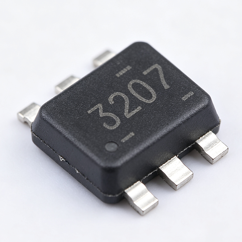
TPS563207DRLR - 3A 17V Synchronous Buck Converter | TI
The Texas Instruments TPS563207DRLR is a simple, easy-to-use 3-A synchronous buck converter in a compact 6-pin SOT-563 (DRL) package measuring just 1.6 mm x 1.6 mm. It accepts an input voltage range of 4.3 V to 17 V and produces an adjustable output down to 0.806 V, making it a space-saving point-of-load power solution. A DC-DC switching regulator (step-down converter) converts a higher input voltage to a lower regulated output using power MOSFET switches, an inductor, and output capacitors. Synchronous buck converters replace the freewheeling diode with a second MOSFET for higher efficiency. Within the power-management IC hierarchy, the TPS563207 is a monolithic buck regulator with integrated high-side and low-side FETs. Key features include D-CAP2 mode control for fast transient response and support of low-ESR output capacitors such as specialty polymer and ultra-low-ESR ceramic types. Fixed-frequency operation in Forced CCM (FCCM) mode maintains small output ripple even at light loads. The 3-A rating with integrated FETs minimizes external component count, and the tiny SOT-563 footprint suits dense PCB layouts. The device is specified from -40C to +125C junction temperature. Internally, D-CAP2 control combines a wide-bandwidth error amplifier with an adaptive on-time generator, enabling near-constant frequency operation and quick response to load steps with minimal output capacitance. Internal compensation and soft-start reduce design effort and board area. Typical applications include 5 V and 12 V rail point-of-load regulation for networking equipment, SSDs and storage, industrial PCs, FPGA/ASIC auxiliary rails, and consumer electronics. The 17-V maximum input covers 12-V buses with margin. Design tip: choose the inductor value and output capacitors per the TI datasheet equations; FCCM mode favors low ripple, while the 0.806-V feedback reference supports low-voltage cores. Verify thermal performance, as the small DRL package dissipates heat mainly through the PCB.
TPS566231 - 6A 18V Sync D-CAP3 Buck Regulator | TI
The Texas Instruments TPS566231 is a cost-effective, high-voltage-input synchronous step-down voltage regulator with integrated FETs, delivering up to 6A of continuous output current. It operates from a 3V to 18V input range, provides an adjustable output down to 0.6V, and comes in a 9-pin PowerVFQFN (RQF) package with pulse skip mode for high light-load efficiency. A synchronous buck converter is a type of DC-DC step-down regulator that uses two integrated transistors (high-side and low-side MOSFETs) to efficiently convert a higher input voltage to a lower output voltage. Unlike asynchronous converters that use a diode for the low-side, synchronous converters replace it with a low-resistance MOSFET, reducing conduction losses and improving efficiency, especially at high output currents. The TPS566231 belongs to the broader family of switching voltage regulators, essential power management ICs that convert and stabilize supply rails in electronic systems. Key features include ultra-low quiescent current (ULQ) for low-bias operation, adjustable soft-start via the SS pin, and up to 98% duty cycle support for low dropout between input and output. Protection is comprehensive: overvoltage protection (OVP), overcurrent protection (OCP), undervoltage lockout (UVLO), overtemperature protection (OTP), and undervoltage protection (UVP) with hiccup mode. The PG (power good) pin is available on the TPS566231P variant for power sequencing in multi-rail systems. The device uses TI's D-CAP3 control architecture, which provides fast transient response without external compensation, simplifying design. Integrated FETs and the compact 9-pin PowerVFQFN package minimize board space, while datasheet efficiency curves show peak efficiency above 90% for typical 12V-to-5V conversions. Typical applications include point-of-load (POL) converters in networking equipment, servers, storage systems, and industrial automation, powering FPGAs, ASICs, and processors where 6A capability and a wide 3V-to-18V input range matter. Pulse skip mode maintains high efficiency at light loads. When designing, select input and output capacitors carefully for stability and low ripple, and use the SS pin to control inrush current during startup.
TPS57140QDGQRQ1 - 42V 1.5A AEC-Q100 Buck Converter | TI
The Texas Instruments TPS57140QDGQRQ1 is an automotive-qualified 42 V, 1.5 A step-down (buck) switching regulator with an integrated 200 mOhm high-side MOSFET, housed in a 10-pin thermally enhanced HVSSOP/MSOP-PowerPAD (DGQ) package. It accepts 3.5 V to 42 V input and produces an adjustable output from 0.8 V to 39 V with peak efficiency at automotive input rails. A DC-DC buck converter is a switching voltage regulator that steps a higher DC voltage down to a lower one using an internal switch, an inductor, and a diode (or synchronous rectifier). Within the power-management hierarchy - voltage regulator -> switching regulator -> step-down converter -> point-of-load regulator - the buck converter is the workhorse of every automotive electronic control unit, converting battery or load-dump-derived rails into clean, efficient low voltages. Key features include AEC-Q100 qualification for 42 V input operation (covering 12 V and 24 V automotive battery systems plus load-dump transients), TI SWIFT (TM) architecture with peak current-mode control for simple external compensation, and Eco-Mode (TM) pulse-skip operation that reduces no-load regulated supply current to just 116 uA. Shutdown current drops to 1.5 uA when the enable pin is pulled low, extending battery life in always-on modules. Technical depth: the current-mode topology provides inherent cycle-by-cycle current limiting, fast transient response, and a single compensation network. The nonsynchronous design (external catch diode) gives freedom to optimize diode voltage rating and thermal placement. The integrated 200 mOhm high-side FET minimizes conduction loss, while the adjustable RT/CLK pin sets switching frequency and supports synchronization to an external clock for EMI-sensitive designs. Typical applications include automotive infotainment and cluster power supplies, camera modules and ADAS sensor rails, body electronics and lighting pre-regulators, and industrial 24 V bus point-of-load conversion. The wide 42 V input rating makes it equally suited to 12 V and 24 V systems without front-end pre-regulation. Design consideration: the nonsynchronous output requires a properly rated Schottky catch diode; at high VIN-to-VOUT ratios, diode loss dominates, so select a 40-60 V Schottky with low reverse leakage at operating temperature. Keep the PowerPAD soldered to a generous ground pour for thermal relief. This page synthesizes distributor pricing, drop-in family alternatives, AEO-optimized FAQs, and practical design notes not found in the manufacturer datasheet, based on data verified 2026-09-10.
TPS57160QDGQRQ1 - 60V 1.5A Buck Converter AEC-Q100 | TI
The Texas Instruments TPS57160QDGQRQ1 is a 1.5 A, 60 V automotive-grade step-down (buck) DC-DC switching regulator with an integrated 200-mohm high-side MOSFET, Eco-Mode control, and an adjustable output from 0.8 V to 58 V, housed in a 10-pin thermally enhanced MSOP-PowerPAD (DGQ) package. A buck converter, or step-down regulator, is a switching power-conversion IC that efficiently reduces a higher input voltage to a lower regulated output by switching an internal or external transistor at high frequency and filtering the result with an inductor and capacitors. Within the power management hierarchy, it sits under DC-DC converters, a subset of voltage regulators, and complements LDOs where conversion efficiency matters more than ultra-low noise. Key features include a wide 3.5 V to 60 V input range with AEC-Q100 automotive qualification, current-mode control that simplifies external compensation, and TI Eco-Mode pulse-skip operation that cuts no-load input supply current to 116 uA. Shutdown supply current via the enable pin is only 1.5 uA, critical for always-connected automotive modules that must minimize quiescent battery drain. Architecturally, the integrated low-drain-to-source on-resistance high-side MOSFET and its gate-drive circuitry inside the package allow high efficiency while keeping junction temperature low at high output currents. Internally fixed undervoltage lockout is set at 2.5 V and is adjustable via the enable pin for tighter input supervision. A RT/CLK pin supports resistor-programmed switching frequency as well as synchronization to an external clock, easing EMI planning in multi-converter systems. Typical applications include automotive 12 V and 48 V battery-rail point-of-load supplies, industrial 24 V bus step-down power, and telecom or avionics wide-input auxiliary rails feeding microcontrollers, CAN transceivers, and sensors. The 60 V rating provides ample surge headroom on load-dump-prone automotive inputs. When designing with this part, keep the PowerPAD soldered to a substantial copper ground plane for thermal performance, and verify compensation network values against the switching frequency chosen. Non-synchronous topology means a proper external catch diode must be selected for peak currents. This page synthesizes distributor pricing, drop-in alternatives, comparison tables, and practical design notes not found in the manufacturer datasheet alone.

TPS60400-Q1 - 60mA Charge Pump Inverter | TI Automotive
The TPS60400-Q1 is an unregulated charge pump voltage inverter from Texas Instruments, designed to generate a negative output voltage from a positive input supply ranging from 1.8 V to 5.25 V. It delivers up to 60 mA of output current and requires only three small 1-µF ceramic capacitors for operation. The device is AEC-Q100 qualified for automotive applications, ensuring reliability in harsh environments. The TPS60400-Q1 features a variable switching frequency that reduces operating current in applications with a wide load range and enables the use of low-value capacitors, making it an efficient and compact solution for generating negative supply rails. A charge pump voltage inverter is a type of DC-DC converter that uses switched capacitors to invert the polarity of an input voltage. Unlike inductive-based converters, charge pumps do not require inductors, which reduces electromagnetic interference (EMI) and simplifies PCB layout. The TPS60400-Q1 belongs to the TPS6040x-Q1 family of charge pump inverters, which are part of the broader category of switching regulators and power management ICs. These devices are essential in systems where a negative supply is needed for analog circuits, such as operational amplifiers, comparators, and data converters. Key features of the TPS60400-Q1 include its wide input voltage range of 1.8 V to 5.25 V, 60 mA output current capability, and low quiescent current due to variable frequency operation. The device operates with a switching frequency that adjusts based on load, optimizing efficiency across the load range. It also features a shutdown mode to reduce power consumption when the output is not needed. The TPS60400-Q1 is available in the small SOT-23 (DBV) package, which is ideal for space-constrained automotive and portable applications. Technically, the TPS60400-Q1 uses a charge pump architecture with an internal oscillator and switching transistors. The variable frequency control reduces switching losses at light loads, improving efficiency. The device can also be configured to generate a doubled positive output (2Vin) or a divided output (Vin/2) by connecting the capacitors differently, providing flexibility in system design. The output is unregulated, so the output voltage tracks the input voltage minus a small drop, which is acceptable for many analog applications. Typical applications include generating a negative rail for operational amplifiers in automotive sensor interfaces, powering LCD bias circuits, and providing a negative supply for audio amplifiers and data converters. The TPS60400-Q1 is also used in battery-powered devices where a negative voltage is required for analog circuitry. Its small footprint and minimal external components make it an attractive choice for compact designs. When designing with the TPS60400-Q1, it is important to place the three 1-µF ceramic capacitors close to the device to minimize parasitic inductance and ensure stable operation. The input capacitor should be placed between the IN pin and ground, and the output capacitor between the OUT pin and ground. The flying capacitor connects between the C1+ and C1- pins. Proper layout is critical to achieve the specified output ripple and efficiency.
TPS61086DRCR - 18.5V 2A Boost Converter 1.2MHz | Texas Instruments
The Texas Instruments TPS61086DRCR is a high-frequency, high-efficiency step-up DC-DC converter with an integrated 2.0-A, 0.13-ohm power switch, capable of providing an output voltage up to 18.5 V. It operates from a 2.3-V to 6.0-V input voltage range and uses a fixed 1.2-MHz pulse-width-modulation (PWM) controller, allowing small external inductors and capacitors and fast transient response. The device is available in a 10-pin VSON (DRC) package with an exposed thermal pad. A boost converter, also known as a step-up converter, is a type of DC-DC switching regulator that produces an output voltage higher than its input voltage. It is a fundamental building block in power management, sitting within the hierarchy of switching regulators, which belong to the broader category of power management integrated circuits (PMICs). Boost converters are essential in battery-powered applications where the battery voltage is lower than the required system rail. Key features include a 2.0-A switch current limit, an adjustable output voltage from 2.8 V to 18.5 V, and a power save mode for improved efficiency at light loads, with the option to force PWM operation. The device also features adjustable soft-start to limit inrush current, thermal shutdown protection, and low quiescent current. The integrated 0.13-ohm switch minimizes conduction losses, contributing to high efficiency across a wide load range. The TPS61086 uses a current-mode control architecture with a fixed 1.2-MHz switching frequency, balancing efficiency and external component size. The high switching frequency enables small, low-profile inductors and ceramic capacitors, reducing overall solution footprint. Power save mode reduces switching frequency at light loads to maintain efficiency, and forced PWM mode supports noise-sensitive applications. Typical applications include battery-powered portable devices, white LED drivers, OLED display bias, and general-purpose step-up voltage regulation. The wide input range and high output capability suit loads requiring voltages above the battery rail. The small package and high efficiency make it ideal for space-constrained designs. When designing with the TPS61086DRCR, ensure proper PCB layout with short, low-inductance paths for the switch node and output capacitor. The exposed pad should be soldered to a large copper area for thermal dissipation, and the inductor saturation current must exceed the peak switch current for stable operation.
TPS610981 - 3.3V Ultra-Low IQ Boost + LDO | Texas Instruments
The Texas Instruments TPS610981 is an ultra-low quiescent current synchronous boost converter with an integrated LDO, providing two regulated output rails from a single low-voltage input. It delivers a fixed 3.3V output and operates from input voltages as low as 0.7V, supporting one-cell alkaline, NiCd, NiMH, coin cell, and one-cell Li-Ion/Li-polymer batteries. The device comes in a compact 6-pin WSON (1.5 mm x 1.5 mm) surface-mount package (DSG suffix). A boost converter is a type of switching DC-DC power supply (part of the broader power management IC hierarchy) that steps an input voltage up to a higher regulated output using an inductor, switching FETs, and a control loop. Unlike a linear regulator, a boost converter can multiply battery voltage, making it essential when system electronics need 3.3V but the cell provides only 1.5V or a discharging Li-Ion cell falls below 3.3V. The TPS61098x family additionally integrates a second low-dropout linear regulator or load switch, eliminating an external LDO and board space. Key features include synchronous rectification for high light-load efficiency, ultra-low quiescent current that extends battery life in always-on systems, integrated output discharge, and power good signaling per TI's product comparison data. The -40C to +85C operating range suits industrial and portable environments. Technically, the synchronous topology removes the external Schottky diode, improving efficiency and reducing BOM count. The two-rail architecture lets designers power a microcontroller rail and a separate sensor or RF rail from one converter with excellent cross regulation. Typical applications include battery-powered sensor nodes, energy harvesting systems, portable medical devices, and low-power IoT endpoints where every microamp of standby current matters. Design consideration: because the input can be driven below 0.7V by a deeply discharged cell, verify minimum input and inrush behavior, and follow TI datasheet (Rev. F) layout guidance for short inductor and output capacitor traces to ensure loop stability.
TPS610981 - 3.3V Ultra-Low Iq Boost + LDO | Texas Instruments
The Texas Instruments TPS610981 is an ultra-low quiescent current synchronous boost converter with an integrated low-dropout linear regulator (LDO), delivering a fixed 3.3V main output plus a secondary LDO rail in a compact 6-pin WSON (1.5x1.5mm) package. It operates from a single-cell alkaline, NiCd, NiMH, coin cell, or Li-Ion battery. A boost converter is a DC-DC step-up topology within the broader voltage regulator family of power management ICs. It raises a lower input voltage to a higher regulated output using an inductor and synchronous switching elements. The TPS61098x family integrates this boost converter with either an LDO or a load switch, providing two output rails from one IC - a key differentiator for space-constrained battery designs. Key features include ultra-low quiescent current of typically 300 nA, extending battery life in standby for years-long deployments. The synchronous boost delivers up to 300 mA at 3.3V from a 1.8V input with efficiency up to 95%, while the integrated LDO supplies a clean, low-noise rail for analog or RF circuitry. True load disconnect during shutdown prevents battery drain, and integrated overcurrent and overtemperature protection ensure robust operation. Architecturally, the device uses pulse-frequency modulation (PFM) at light loads to minimize quiescent current, transitioning to PWM at heavier loads for low ripple and stable regulation. The LDO is powered from the boost output, generating a second rail with no additional magnetics. Typical applications include wireless sensor nodes, hearing aids, portable medical devices, and IoT endpoints where the 3.3V rail powers microcontrollers and RF transceivers while the LDO rail feeds analog sensors or audio codecs. For design, select the recommended 2.2 uH inductor and place input/output capacitors close to the pins to minimize ripple and preserve the ultra-low standby current advantage.
TPS61230 - 5A Synchronous Boost Converter | Texas Instruments
The Texas Instruments TPS61230 is a high-efficiency synchronous step-up (boost) converter with an integrated 5-A switch, designed for products powered by a one-cell Li-Ion battery or a regulated 3.3-V rail. It provides an adjustable output voltage via an external resistor divider, with a typical input range of 2.5 V to 4.5 V and output up to 5 V. The device is available in a compact 3-mm x 3-mm VQFN-10 (DRC) package, enabling space-constrained designs. A boost converter, also known as a step-up converter, is a type of DC-DC switching regulator that produces an output voltage higher than its input voltage. It belongs to the broader family of switching voltage regulators, which are essential in power management ICs for efficiently converting and regulating electrical power. Unlike linear regulators, boost converters use an inductor and switches to transfer energy, achieving high efficiency even with large input-to-output voltage differences. Key features of the TPS61230 include a 5-A switch current limit, up to 96% efficiency, and automatic power-save mode for light loads, which reduces quiescent current to 20 µA. The device also offers overcurrent, overvoltage, and thermal shutdown protection. Its low RDS(on) switches minimize conduction losses, making it suitable for battery-powered applications where efficiency is critical. Technically, the TPS61230 uses a fixed-frequency PWM control scheme with a typical switching frequency of 1.5 MHz, allowing the use of small external components. The adjustable output is set with a resistor divider from the FB pin, and the device supports a soft-start function to limit inrush current. The integrated synchronous rectifier eliminates the need for an external Schottky diode, reducing component count and board space. Typical applications include portable electronics, battery-powered devices, and systems requiring a regulated 5-V rail from a lower voltage source. The TPS61230 is ideal for USB-powered devices, LED drivers, and sensor nodes where efficiency and small size are paramount. When designing with the TPS61230, ensure proper PCB layout with short, wide traces for high-current paths and adequate input/output capacitance to minimize voltage ripple. The inductor value should be selected based on the switching frequency and load current to maintain stable operation.
TPS62090 - 3A, 6V Synchronous Step-Down Converter | TI
The Texas Instruments TPS62090 is a high-frequency synchronous step-down (buck) converter optimized for small solution size and high efficiency in battery-powered applications. It operates from an input voltage range of 2.5 V to 6 V and delivers up to 3 A of continuous output current. The output voltage is adjustable from 0.8 V to VIN using external resistors, with a typical configuration of 1.8 V. The device is available in a 16-pin VQFN (RGT) package with an exposed thermal pad, enabling compact PCB layouts. A synchronous step-down converter is a type of DC-DC switching regulator that steps down a higher input voltage to a lower output voltage with high efficiency. Unlike linear regulators, which dissipate excess power as heat, switching converters use high-frequency switching and energy storage elements (inductors and capacitors) to transfer energy with minimal loss. The TPS62090 belongs to the TPS6209x family of synchronous buck converters within the broader power management IC category used in portable, industrial, and automotive power rails. Key features include the proprietary DCS-Control topology, which combines voltage-mode and current-mode control to deliver excellent load transient response and accurate output regulation. The converter achieves up to 97% efficiency and operates at a nominal 2.8 MHz switching frequency (1.4 MHz in some modes), allowing small inductors. Power Save Mode reduces quiescent current to approximately 20 uA at light loads, and 100% duty cycle support enables the lowest dropout operation. Technically, the DCS-Control architecture enables seamless PWM-to-PFM transition, maintaining high efficiency across the full load range. Soft-start, enable, and power-good pins allow flexible power sequencing and voltage tracking configurations. Only a small inductor and ceramic capacitors are required; the 3x3 mm VQFN-16 package suits space-constrained designs. Typical applications include point-of-load (POL) supplies for processors, FPGAs, and DSPs; power rails for smartphones, tablets, and other portable battery-powered devices; and industrial systems requiring high efficiency in a small footprint. When designing with the TPS62090, observe the minimum output capacitance required by the DCS-Control topology for stability, minimize parasitic inductance in the power loop, and provide adequate copper area under the exposed pad for thermal dissipation.
TPS62130RGTR - 3A 3-17V Buck Converter 2.5MHz | Texas Instruments
The Texas Instruments TPS62130RGTR is a synchronous step-down (buck) DC-DC converter delivering up to 3A output current from a 3V to 17V input supply in a compact 16-pin VQFN (3x3 mm) package with exposed thermal pad, ideal for space-constrained point-of-load power management. A buck converter, or step-down converter, is a switching voltage regulator that efficiently reduces a higher input voltage to a lower regulated output. It is a fundamental power management IC building block, converting energy from 12V rails, batteries, or unregulated sources into the low-voltage rails required by processors, FPGAs, and sensors. Key features include an adjustable output from 0.9V to 6V, a 2.5MHz switching frequency, and approximately 17uA quiescent current in power-save mode. Integrated synchronous rectification eliminates the external Schottky diode and improves efficiency. The device provides an enable pin, open-drain power-good output, and soft-start/tracking pin for controlled startup and power sequencing. Technically, the TPS62130 uses DCS-Control (Direct Control with Seamless transition into Power Save Mode) topology, combining voltage-mode and current-mode control for excellent load and line regulation with seamless PWM/power-save transitions across the load range. The 2.5MHz switching frequency permits small inductors and capacitors, shrinking the total solution footprint. Overcurrent and overtemperature protection ensure robust operation. Typical applications include standard 12V rail POL supplies, converters from single or multiple Li-ion battery stacks, solid-state drives, embedded systems, and LDO replacements where efficiency matters. High efficiency across light and heavy loads suits battery-powered portable devices, industrial control, and networking equipment. Design tip: place input and output capacitors close to the pins to minimize parasitic inductance, solder the exposed pad to a thermal relief pattern, and use the SS/TR pin to set the output ramp or implement voltage tracking.
TPS62134D - 3.2A 17V Step-Down Converter | Texas Instruments
The Texas Instruments TPS62134D is a 17-V input synchronous step-down DC-DC converter delivering up to 3.2A of output current from a 3x3 mm 16-pin VQFN package with exposed thermal pad. The output voltage is adjustable down to 0.7V, and the device includes a low-power mode input designed specifically for Intel Skylake platform applications such as Ultrabooks and notebooks. A buck (step-down) switching regulator is a type of DC-DC converter that converts a higher input voltage to a lower regulated output using a high-side and low-side power MOSFET switch, an inductor, and capacitors. Within the power management hierarchy, the TPS62134 belongs to the switching voltage regulator family, sitting between point-of-load converters and full PMIC solutions. Its D-CAP-style synchronous architecture eliminates external bootstrap concerns for the low-side FET and improves efficiency at light load. Key features include the wide 17V maximum input supporting multi-cell and adapter rails, 3.2A continuous output current, a low-power mode input pin that lets the system MCU force efficiency-optimized light-load operation, and output voltage adjustability from 0.7V with a single external resistor divider. The 3x3 mm VQFN-16 (RGT) footprint keeps solution height low for ultraportable designs, and internal compensation simplifies design-in. Technically, the TPS62134 uses a synchronous rectification topology that reduces conduction losses compared to asynchronous (external-diode) bucks, and its control loop supports fast transient response for CPU core rails. The Intel Skylake compatibility makes it a natural fit for notebook VCCSA/VCCCORE auxiliary rails where dynamic load steps are frequent. Typical applications include Ultrabook and notebook point-of-load supplies, tablet and convertible power trees, SSD and storage-card supplies, and general 5V/12V-rail point-of-load conversion up to 3.2A. Design consideration: keep the input loop (input capacitor, VIN pins, PGND) as tight as possible; at 3.2A, switch-node ringing drives EMI, and a well-placed 22uF input ceramic plus short PGND return is essential per the TPS62134x datasheet (Rev. E) layout guidelines.
TPS62150A-Q1 - 3-17V 1A Automotive Step-Down Converter | TI
The TPS62150A-Q1 is an automotive-grade synchronous step-down DC-DC converter from Texas Instruments, designed for high power density applications. It operates from an input voltage range of 3 V to 17 V and delivers up to 1 A of output current with an adjustable output voltage from 0.9 V to 6 V. The device is available in a 3 mm × 3 mm QFN package (16-pin VQFN), making it suitable for space-constrained automotive and industrial designs. A step-down converter, also known as a buck converter, is a type of DC-DC converter that efficiently reduces a higher input voltage to a lower output voltage. It is a fundamental building block in power management systems, converting raw battery or bus voltages to the precise levels required by microcontrollers, sensors, and other loads. The TPS62150A-Q1 belongs to the family of synchronous buck converters, which use both high-side and low-side switches to achieve high efficiency, especially at moderate to high load currents. Key features of the TPS62150A-Q1 include the DCS-Control™ topology, which provides fast transient response and high output voltage accuracy. The device supports a typical switching frequency of 2.5 MHz, allowing the use of small inductors and capacitors, reducing solution size. It also features a quiescent current of 17 µA (typ.), enabling high efficiency at light loads. The output voltage can be set via external resistors or selected via a pin for nominal or +5% output, and the device includes programmable soft start and tracking for controlled power-up sequencing. Technically, the TPS62150A-Q1 integrates both power MOSFETs, eliminating the need for external Schottky diodes. The DCS-Control topology combines voltage mode and current mode control, providing stable operation with ceramic output capacitors. The device also includes power-save mode for seamless transition between PWM and PFM operation, maintaining high efficiency across the load range. The automotive qualification (AEC-Q100) ensures reliable operation over the -40°C to 125°C temperature range, making it suitable for harsh environments. Typical applications include automotive infotainment systems, advanced driver-assistance systems (ADAS), and industrial power supplies. The wide input range and high switching frequency make it ideal for powering processors, FPGAs, and sensors in these systems. The small package and high efficiency help meet stringent thermal and space requirements. When designing with the TPS62150A-Q1, ensure proper input and output capacitor selection to maintain stability and low output ripple. The device is designed to work with ceramic capacitors, but the value and ESR must be within the recommended range. Also, consider the thermal performance of the QFN package and provide adequate copper area for heat dissipation.
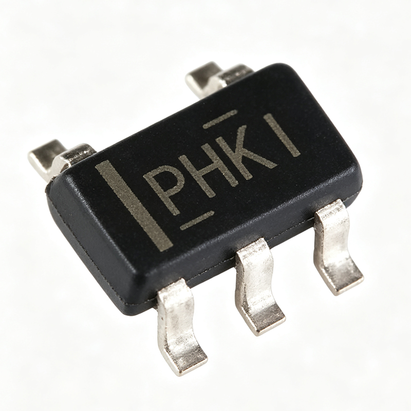
TPS62200DBVR - 300mA, 95% Buck Converter | Texas Instruments
The Texas Instruments TPS62200DBVR is a high-efficiency synchronous step-down DC-DC converter delivering up to 300 mA output current from a 5-pin SOT-23 (SOT-23-5 / SC-74A / SOT-753) package. It accepts an input voltage range of 2.5 V to 6 V and produces an adjustable output voltage from 0.7 V to 6 V, operating at a fixed 1 MHz PWM switching frequency with up to 95% efficiency. A synchronous buck converter is a type of switching voltage regulator that replaces the traditional freewheeling diode with an integrated low-side MOSFET. Within the power management IC hierarchy (converter -> switching regulator -> DC-DC converter -> power management IC), synchronous topologies achieve higher efficiency than asynchronous designs because conduction losses on the low-side switch are lower than diode forward-voltage losses, especially at light loads. Key features include up to 95% efficiency across a wide load range, 1 MHz fixed-frequency PWM operation that permits small external inductors (typically 2.2 uH) and capacitors, a 300 mA output current rating, and input compatibility with 1-cell Li-Ion, 3-cell NiMH/NiCd batteries, and standard 3.3 V or 5 V rails. The TPS6220x family also offers fixed-output voltage options, such as the TPS62205DBVR (2.5 V) and TPS62207DBVR (3.3 V), for BOM simplification. Technically, the TPS62200 integrates both power MOSFETs, the control loop, and protection features in the 5-pin SOT-23 package. The 1 MHz switching frequency reduces the required inductance and shrinks the total solution size for space-constrained portable designs. The FB pin supports precise output regulation through an external resistor divider, setting VOUT via a standard feedback network. Typical applications include powering low-voltage DSPs and microcontrollers in portable systems, battery-powered point loads in Li-Ion handheld devices, and local point-of-load conversion from 3.3 V or 5 V rails in industrial and consumer electronics. Design tip: keep the input and output ceramic capacitors (typically 4.7 uF) close to the VIN and SW pins, and choose the adjustable version only when no fixed-output variant of the TPS6220x family matches your rail voltage. This page synthesizes distributor pricing, drop-in alternatives, comparison tables, and practical design notes not found in the manufacturer datasheet.
TPS62590DRVR - 2.25MHz 1A Step-Down Converter | Texas Instruments
The Texas Instruments TPS62590DRVR is a high-efficiency synchronous step-down (buck) converter optimized for battery-powered portable applications. It delivers up to 1A output current from a single Li-Ion cell or 2-3 AA/AAA batteries, with an input voltage range of 2.5V to 5.5V. The device is available in a compact 6-pin WSON (2mm x 2mm) package with exposed thermal pad, making it ideal for space-constrained designs. A step-down converter, also known as a buck converter, is a type of DC-DC switching regulator that steps down an input voltage to a lower output voltage with high efficiency. Unlike linear regulators, which dissipate excess power as heat, switching regulators use inductive energy storage to achieve efficiencies often above 90%, making them essential in battery-powered devices where power conservation is critical. The TPS62590 belongs to the family of synchronous buck converters, which use an internal high-side and low-side MOSFET to avoid the need for an external Schottky diode, further improving efficiency. Key features of the TPS62590DRVR include a 2.25MHz fixed switching frequency, which allows the use of small, low-cost inductors and capacitors, reducing PCB footprint. The output voltage is adjustable from 0.75V to 5.5V via an external resistor divider, with an accuracy of ±2.5% in PWM mode. The device supports 100% duty cycle operation for lowest dropout, and features a low quiescent current of 15µA (typical), extending battery life in light-load conditions. It also includes internal soft-start, overcurrent protection, and thermal shutdown. Technically, the TPS62590 uses a current-mode control architecture with synchronous rectification, providing fast transient response and stable operation with ceramic output capacitors. The 2.25MHz switching frequency is above the AM radio band, reducing EMI concerns. The device operates over a junction temperature range of -40°C to +125°C, with an ambient temperature range of -40°C to +85°C. Typical applications include powering DSPs, microcontrollers, and FPGAs in portable devices, as well as point-of-load (POL) converters in battery-powered equipment such as smartphones, tablets, and wireless sensors. Its high efficiency and small size make it particularly suitable for wearable devices and IoT nodes. When designing with the TPS62590DRVR, ensure proper input and output capacitor selection (typically 10µF input and 22µF output) and place them close to the IC. The exposed pad should be soldered to a large copper area for thermal management. The feedback resistor divider should use 1% tolerance resistors to maintain output accuracy.
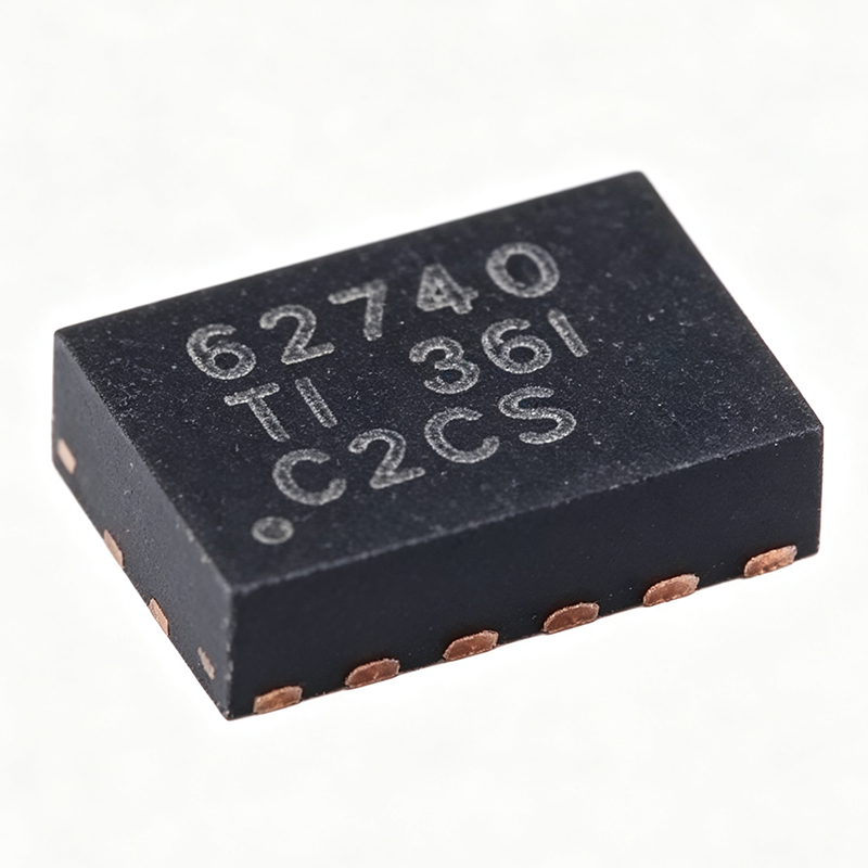
TPS62740DSSR - 300mA 360nA Iq Buck Converter | Texas Instruments
The Texas Instruments TPS62740DSSR is an ultra-low-power step-down buck DC-DC converter delivering up to 300mA output current from a 2.2V to 5.5V input, housed in a compact 12-pin 2x3mm WSON (DSS) package with exposed pad. It is purpose-built for battery-powered Bluetooth Low Energy (BLE) and wireless sensor applications, featuring a typical quiescent current of only 360nA. A step-down (buck) converter is a switching voltage regulator that efficiently converts a higher input voltage to a lower output voltage using a switch, inductor, and capacitor. Within the power management IC hierarchy, it belongs to the DC-DC converter family, which achieves far higher efficiency than linear regulators by storing and transferring energy rather than dissipating it as heat. This makes buck converters the preferred choice for extending battery life in portable and IoT systems. Key features include up to 90% efficiency at just 10uA output current, RF-friendly DCS-Control topology, and a switching frequency of up to 2MHz, which permits a tiny 2.2uH inductor and 10uF output capacitor for a total solution size of approximately 31mm2. The device also integrates a load switch, enabling system power gating of downstream circuitry to further reduce standby current. The DCS-Control (Direct Control with Seamless Transition into Power Save Mode) architecture combines the low output ripple of PWM operation with the high light-load efficiency of PFM power-save mode, transitioning seamlessly without transient excursions. This is critical for RF power rails, where ripple and spurious noise can degrade transmitter phase noise and receiver sensitivity. Compared with conventional power-save-mode converters, the seamless transition means output impedance stays low across the entire load range, preserving output-voltage accuracy from full load down to nanoamp quiescent levels. Typical applications include BLE beacons and sensors, energy harvesting systems, wearable devices, and battery-powered metering, where a single lithium or alkaline cell must power the system for months or years. With 360nA quiescent current, a coin cell (approx. 220mAh) can support a duty-cycled sensor node for several years in standby-dominated operation. Design consideration: optimize the output capacitor ESR and inductor value per the TI datasheet recommendation (2.2uH, 10uF) to preserve the low-ripple, RF-friendly behavior in power-save mode. This page synthesizes distributor pricing, drop-in alternatives, and practical design notes not found in the manufacturer datasheet.