Interface ICs
Subcategories
Products (181)

GX39221-DNT - 96Gbaud 2-Ch Linear TIA | Renesas | 800G Coherent
The Renesas Electronics GX39221-DNT is a dual-channel 96Gbaud linear transimpedance amplifier (TIA) engineered for 800G and beyond integrated coherent receivers (ICRs), integrating two TIA signal paths for the I and Q channels in a compact package (DNT suffix). This telecom IC enables small form factor (SFF) integrated optical modules such as CFP2 and CFP4. A transimpedance amplifier is an amplifier that converts input current from a photodiode into an output voltage, characterized by gain expressed in ohms. Within the signal chain hierarchy, the TIA sits directly after the photodiode in an optical receiver, feeding subsequent linear equalizers, drivers, and analog-to-digital converters (ADCs) in the power management and telecom IC ecosystem. In coherent optical communications, linear TIAs preserve waveform linearity so that digital signal processors (DSPs) can apply chromatic dispersion compensation and advanced modulation decoding. Key features of the GX39221 include its 96Gbaud per-channel bandwidth class, dual-channel integration for I and Q polarization-multiplexed coherent detection, linear (non-limiting) transfer characteristics essential for coherent DSP-based receivers, and a low-power, compact design suited to SFF modules. Integration of two signal paths reduces part count and simplifies alignment in CFP2 and CFP4 module designs. Technically, the GX39221 targets integrated coherent receiver architectures where photodiode photocurrent from coherent detection is amplified with high linearity at extreme symbol rates. Linear TIAs at 96Gbaud require high transimpedance gain, low noise, wide bandwidth, and output swing matched to downstream linear equalizers. The GX39221-DNT variant suffix denotes a specific package/packing configuration per Renesas ordering codes. Typical applications include 800G and beyond coherent transceivers, integrated coherent receivers (ICRs), CFP2-DCO and CFP4 optical modules, and data center interconnect (DCI) links. The dual-channel structure directly matches the I/Q detection scheme of polarization-multiplexed coherent receivers. Design consideration: linear TIAs for coherent receivers demand careful RF layout, matched differential routing, and impedance control between the photodiode, TIA, and downstream linear equalizer; consult the manufacturer datasheet for the exact differential output interface and supply requirements. This page synthesizes distributor pricing from LCSC, DigiKey, and Mouser, datasheet availability, and application context not found on any single distributor page.

ISO6762FDWR - 6-Channel Digital Isolator 50Mbps | TI
The ISO6762FDWR is a general-purpose, six-channel digital isolator from Texas Instruments, featuring a 4/2 channel configuration (four forward, two reverse) and supporting data rates up to 50 Mbps. It provides reinforced isolation with a withstand voltage of 5000 Vrms and a common-mode transient immunity (CMTI) of 50 kV/µs, ensuring robust performance in noisy industrial environments. The device operates over a wide supply voltage range of 1.8V to 5.5V on both sides, making it compatible with low-voltage logic and legacy 5V systems. Housed in a 16-pin SOIC (DW) package with 7.50mm width, it is designed for surface-mount assembly and is qualified for operation from -40°C to 125°C. Digital isolators are components that provide galvanic isolation between two circuit domains while allowing digital signals to pass across the isolation barrier. They are essential in applications where ground potential differences, noise, or safety requirements demand separation, such as in industrial automation, motor drives, and medical equipment. The ISO6762FDWR uses capacitive isolation technology, which offers high-speed data transfer with low power consumption and excellent EMC performance, as highlighted in the datasheet. Key features of the ISO6762FDWR include its 50 Mbps data rate, which supports high-speed protocols like SPI and RS-485, and its 1.8V logic support, enabling direct interface with low-voltage microcontrollers. The device also features an enable pin for output control, fail-safe outputs that default to a known state when inputs are unpowered, and a wide temperature range. Its reinforced isolation rating ensures reliable operation in safety-critical applications. The ISO6762FDWR is built on TI's capacitive isolation technology, which uses high-voltage capacitors to couple signals across the barrier. This architecture provides low propagation delay and high CMTI, making it suitable for applications where fast transients are present. The device also includes integrated noise filtering to enhance signal integrity. Typical applications include isolating SPI, RS-232, RS-485, and CAN buses in industrial control systems, motor drives, and power converters. Its high data rate and robust isolation make it ideal for communication interfaces in factory automation and building automation. When designing with the ISO6762FDWR, ensure proper PCB layout with adequate clearance and creepage distances under the isolator to maintain the rated isolation voltage. Also, place decoupling capacitors close to the VCC pins to minimize noise.
ISO6763DWR - 6-Ch 50Mbps 5000Vrms Digital Isolator | TI
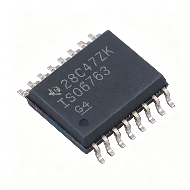
The Texas Instruments ISO6763DWR is a general-purpose six-channel (3/3) reinforced digital isolator with a 50 Mbps data rate, 5000 VRMS isolation rating, and 1.8 V logic support, housed in a 16-pin SOIC (DW, 7.50 mm width) package rated from -40C to +125C. A digital isolator is a semiconductor device that transfers digital signals across an isolation barrier without any galvanic connection, replacing optocouplers in the signal-isolation hierarchy of industrial interface and power-management systems. Reinforced digital isolators use a capacitive or transformer-based barrier certified to withstand thousands of volts, enabling safe communication between controllers and high-voltage circuitry in compliance with reinforced-insulation system requirements. The ISO6763DWR's key features include a 50 Mbps maximum data rate for high-throughput SPI, RS-485, CAN, and RS-232 links; a robust isolation barrier with up to 5000 VRMS isolation rating, 1500 VRMS working voltage, up to 10 kV surge capability, and high CMTI (50 kV/us minimum per distributor listings, up to 150 kV/us typical per the ISO676x datasheet); and a wide dual-supply range of 1.71 V to 1.89 V on one side and 2.25 V to 5.5 V on the other, allowing direct interfacing with 1.8 V logic. The device uses TI's proven capacitive isolation construction with an SiO2 dielectric barrier, delivering long barrier lifetime at 1500 VRMS working voltage and robust EMC performance against common-mode transients. The symmetrical 3-forward/3-reverse channel configuration supports bidirectional buses such as full-duplex RS-485 and isolated SPI with independent read-back. Typical applications include isolated CAN, RS-232, and RS-485 industrial fieldbus nodes, isolated SPI communication in battery management and motor-drive systems, and isolation of PLC I/O modules in factory automation. Designers should bypass both VCC pins with 0.1 uF and 1 uF ceramic capacitors placed as close to the package as possible, and verify that the logic-side supply domain matches the 1.71 V to 1.89 V narrow range of the low-voltage side. This page adds distributor pricing tiers, drop-in alternatives, and engineering design notes beyond what the manufacturer datasheet provides.
ISO6763FDWR - 6-Ch 5kVrms Digital Isolator 50Mbps | TI
The Texas Instruments ISO6763FDWR is a general-purpose six-channel reinforced digital isolator delivering 50 Mbps signaling rate and 5000 Vrms isolation per UL 1577, housed in a 16-pin SOIC (DW, 7.50 mm width) package. It provides a 3/3 channel configuration (three forward, three reverse channels) with 50 kV/us common-mode transient immunity and support for 1.8V, 2.5V, 3.3V, and 5V CMOS/LVCMOS logic on both sides. A digital isolator is a semiconductor device that transfers digital signals across an isolation barrier using high-frequency carrier-based or edge-based encoding, replacing optocouplers with faster, more reliable, and more power-efficient capacitive isolation. Digital isolators sit within the signal isolation hierarchy of industrial interface components, alongside isolated transceivers and isolated gate drivers, and are fundamental to galvanic isolation in power management and communication systems. Key features of the ISO6763FDWR include the 50 Mbps maximum data rate, a high 50 kV/us CMTI that maintains signal integrity in electrically noisy environments such as motor drives, and reinforced isolation rated to 5000 Vrms per UL 1577 with additional VDE, TUV, CSA, and CQC certifications. The device offers high electromagnetic immunity and low emissions at low power consumption, per the TI ISO676x family datasheet. Architecturally, the ISO676x family uses TI capacitive isolation technology with on-chip transformers formed from SiO2, providing a robust insulation barrier that is resistant to magnetic field interference and field aging, unlike optocoupler LED-based approaches. The F suffix grade of the ISO6763 carries the default default characteristic; the six channels are split symmetrically 3/3, allowing bidirectional signal transfer in a single package without extra components. Typical applications include isolated RS-485 and RS-232 communication links, isolated SPI buses in industrial programmable logic controllers, CAN isolation in factory automation, and battery management systems where multi-bit status signals must cross a safety barrier. When designing with this device, ensure both VCC1 and VCC2 supplies are decoupled with 0.1 uF ceramic capacitors placed close to the pins, and verify that the default output states match the system fail-safe requirements. This page synthesizes distributor pricing, drop-in family alternatives, and practical design notes not found in the manufacturer datasheet.
ISO6763FQDWRQ1 - 6-Ch 50Mbps Digital Isolator 5kVrms | TI
The Texas Instruments ISO6763FQDWRQ1 is an automotive-grade, six-channel (3/3 configuration) reinforced digital isolator delivering up to 50 Mbps data rate, 5000 Vrms galvanic isolation per UL 1577, and 100 kV/us common-mode transient immunity, housed in a 16-pin wide-body SOIC (DW) package rated from -40C to +125C. A digital isolator is a semiconductor device that transfers digital signals across an isolation barrier while blocking high voltages, ground loops, and common-mode transients. Within the power and signal-chain hierarchy, it sits between level translators and optocouplers: unlike optocouplers, capacitive or inductive digital isolators provide far higher data rates, tighter channel-to-channel matching, longer lifetime, and lower power consumption, making them the modern choice for galvanic isolation in industrial and automotive systems. Key features include support for 1.8 V, 2.5 V, 3.3 V, and 5 V logic on either side of the barrier, robust EMC performance with 100 kV/us CMTI for harsh motor-drive environments, and a symmetric 3/3 channel arrangement that suits bidirectional buses such as SPI and general-purpose parallel signaling. The automotive Q1 qualification and AEC-Q100-grade temperature range address under-hood and traction-battery requirements. Architecturally, the ISO676x family uses TI's silicon-dioxide isolation barrier with on-chip RF oscillators and data coding to transmit across the capacitive barrier with deterministic propagation delay and high immunity to external fields. The wide-body 16-pin SOIC (DW) package is a pin-to-pin upgrade to older TI generations, easing drop-in redesigns, and its 8 mm creepage/clearage supports reinforced isolation ratings per UL 1577. Typical applications include isolated SPI communication in battery management systems, industrial PLC digital I/O isolation, motor-drive gate-drive supervisory links, and isolated interfaces between microcontrollers and field-side sensors. When designing, keep total data rate within 50 Mbps and verify the supply range on each side independently, since the two sides support different logic levels by design. This page synthesizes distributor pricing, drop-in alternatives, and practical design notes not found in the manufacturer datasheet.
ISO7241MDW - 4-Ch 3/1 150Mbps Digital Isolator | TI
The ISO7241MDW is a quad-channel digital isolator from Texas Instruments, featuring a 3/1 channel configuration (three forward and one reverse) with a signaling rate of 150 Mbps. It is housed in a 16-pin SOIC (DW) package with a wide body (7.50 mm width). The device provides galvanic isolation up to 2500 Vrms and a common-mode transient immunity (CMTI) of 25 kV/µs, making it suitable for industrial and automotive applications where robust isolation is required. Digital isolators are components that transfer digital signals across an isolation barrier while preventing DC current flow and rejecting common-mode noise. They are essential in systems where safety, noise immunity, or ground potential differences exist between circuit domains. The ISO7241MDW uses a silicon-dioxide (SiO2) isolation barrier, which offers high reliability and long-term stability. It is part of the ISO7240x/ISO7241x/ISO7242x family of quad-channel isolators, which provide various channel configurations and output-enable functions. Key features of the ISO7241MDW include a low channel-to-channel output skew of 1 ns maximum, low pulse-width distortion (PWD) of 2 ns maximum, and low jitter content of 1 ns typical at 150 Mbps. The device operates over a wide supply voltage range of 3.0 V to 5.5 V on both sides, and it is specified for the industrial temperature range of -40°C to +125°C. The output-enable function allows the outputs to be placed in a high-impedance state, facilitating bus-oriented applications. The ISO7241MDW is designed for high-speed signal isolation in applications such as industrial fieldbus communication, motor control, power inverters, and isolated SPI/UART interfaces. Its high CMTI ensures reliable operation in noisy environments, and the 2500 Vrms isolation rating meets basic insulation requirements for many industrial standards. The device is RoHS compliant and lead-free, supporting environmentally conscious designs. When designing with the ISO7241MDW, it is important to provide adequate decoupling capacitors on both supply pins and to ensure proper PCB layout to maintain signal integrity and isolation performance. The device does not require external components for the isolation barrier, simplifying the design. For applications requiring higher isolation or different channel configurations, other members of the ISO724x family can be considered.
ISO7721BDWR - 2Ch Reinforced Digital Isolator | TI
The ISO7721BDWR is a high-speed, robust EMC, reinforced dual-channel digital isolator from Texas Instruments. It provides 5000 Vrms isolation per UL 1577, with a data rate of 100 Mbps and common-mode transient immunity (CMTI) of 85 kV/µs. The device is available in a 16-pin SOIC (DW) package with 7.50 mm width, operating over a temperature range of -55°C to +125°C. It is designed for applications requiring reliable signal isolation in industrial, automotive, and communication systems. Digital isolators are components that transmit digital signals across an isolation barrier, providing galvanic isolation to protect circuits and users from high voltages, ground loops, and noise. They are essential in systems where safety and signal integrity are critical, such as in motor drives, power supplies, and medical equipment. The ISO7721BDWR belongs to the ISO772x family, which includes reinforced and basic insulation variants, offering flexibility for different isolation requirements. Key features of the ISO7721BDWR include its reinforced insulation rating, 100 Mbps data rate, and 85 kV/µs CMTI, which ensures reliable operation in noisy environments. The device supports CAN, RS232, and RS485 protocols, making it versatile for industrial communication. It also features low power consumption and a wide supply voltage range, enhancing its suitability for power-sensitive designs. Technically, the ISO7721BDWR uses TI's capacitive isolation technology, which provides robust performance against magnetic interference and ensures long-term reliability. The device has a channel configuration of 1/1 (one forward, one reverse), allowing bidirectional communication. It also includes an enable pin for power management and failsafe outputs for safety-critical applications. Typical applications include industrial fieldbus communication, isolated SPI/UART interfaces, motor control, and power converters. The high CMTI and reinforced isolation make it ideal for harsh environments where voltage transients are common. When designing with the ISO7721BDWR, ensure proper PCB layout with adequate creepage and clearance distances to maintain the isolation rating. Place decoupling capacitors close to the power pins and follow the recommended layout guidelines in the datasheet to achieve optimal EMC performance.
ISO7721DW - 2Ch Reinforced Digital Isolator 100Mbps | TI
The ISO7721DW is a high-performance, dual-channel digital isolator from Texas Instruments, designed to provide robust signal isolation in industrial and automotive applications. It delivers 5000 Vrms isolation per UL 1577, with a data rate of 100 Mbps and a common-mode transient immunity (CMTI) of 85 kV/µs. The device is available in a 16-pin SOIC (DW) package with a wide body width of 7.50 mm, ensuring adequate creepage and clearance for reinforced insulation. Digital isolators are essential components that transfer digital signals across an isolation barrier, preventing dangerous voltages or ground loops from affecting sensitive circuitry. They replace optocouplers in many designs, offering higher speed, better reliability, and lower power consumption. The ISO7721DW belongs to the ISO772x family, which includes devices with reinforced insulation ratings certified by VDE, CSA, TUV, and CQC, in addition to UL 1577. Key features of the ISO7721DW include a dual-channel configuration with one forward and one reverse channel (1/1), a wide supply voltage range of 2.25 V to 5.5 V, and a default output state that is high when the input is unpowered. The device supports both 3.3 V and 5 V logic levels, making it versatile for mixed-voltage systems. Its robust EMC performance ensures reliable operation in noisy industrial environments. The ISO7721DW uses TI's capacitive isolation technology, which provides superior immunity to magnetic interference compared to traditional optocouplers. The isolation barrier is rated for 5000 Vrms, with a working voltage of 800 Vrms (reinforced) or 566 Vrms (basic), depending on the certification. The device also features a fail-safe output that defaults to a known state if the input side loses power, enhancing system safety. Typical applications include industrial fieldbus communication (e.g., PROFIBUS, Modbus), motor drives, power inverters, and isolated SPI/UART interfaces. The high CMTI of 85 kV/µs makes it suitable for applications with fast-switching power stages, such as SiC and GaN inverters, where transient noise can corrupt signals. When designing with the ISO7721DW, ensure proper PCB layout with adequate isolation spacing and place decoupling capacitors close to the VCC pins. The device supports a wide temperature range of -55°C to +125°C, making it suitable for harsh environments.
ISO7721FQDWRQ1 - Automotive Reinforced 2-Ch Digital Isolator | TI
The ISO7721FQDWRQ1 is an automotive-grade, reinforced dual-channel digital isolator from Texas Instruments, designed for high-speed signal isolation in harsh automotive and industrial environments. It provides 5000 Vrms isolation voltage, supports data rates up to 100 Mbps, and features a high common-mode transient immunity (CMTI) of 85 kV/µs. The device is offered in a 16-pin SOIC (DWR) package with 7.50 mm width, suitable for surface-mount assembly. Digital isolators are components that transmit digital signals across an isolation barrier, providing galvanic isolation to protect circuits and users from high voltages, ground loops, and noise. They are essential in systems where safety and signal integrity are critical, such as in electric vehicles, industrial motor drives, and medical equipment. The ISO7721FQDWRQ1 belongs to the ISO772x-Q1 family, which is part of TI's broad portfolio of isolation products. Key features include a reinforced isolation rating per VDE 0884-10 and UL 1577, a default output state of low (suffix F) when input power is lost, and a wide supply voltage range of 2.25 V to 5.5 V. The device also offers a 1/1 channel configuration (one forward, one reverse), making it ideal for bidirectional isolation. Its robust EMC performance ensures reliable operation in noisy environments. The ISO7721FQDWRQ1 uses TI's capacitive isolation technology, which provides low power consumption and high-speed operation. The device is AEC-Q100 qualified for automotive applications, ensuring reliability under extreme temperature and vibration conditions. It also features an enable pin for output control and a fail-safe mechanism that sets outputs to a known state during power loss. Typical applications include isolated SPI, UART, and CAN interfaces in automotive battery management systems, on-board chargers, and industrial fieldbus communication. The high CMTI and reinforced isolation make it suitable for motor drive inverters and power converters where fast switching transients are present. When designing with this device, ensure proper PCB layout with adequate creepage and clearance distances to maintain isolation ratings. Place decoupling capacitors close to the VCC pins and follow the recommended layout guidelines in the datasheet to achieve optimal EMC performance.
ISO7741FDBQR - 4-Ch 100Mbps Digital Isolator | Texas Instruments
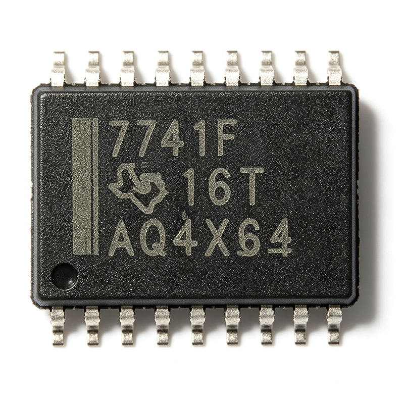
The Texas Instruments ISO7741FDBQR is a high-performance, reinforced quad-channel digital isolator designed for robust signal isolation in industrial and automotive systems. It provides four isolation channels in a 3 forward / 1 reverse configuration, supports data rates up to 100 Mbps, and achieves a common-mode transient immunity (CMTI) of 85 kV/us. Housed in a compact 16-pin SSOP (DBQ) package, the device delivers 3000 Vrms reinforced isolation per UL 1577 and operates from -55C to +125C. A digital isolator is an integrated circuit that transfers digital signals across an isolation barrier without a direct electrical connection, preventing ground loops and protecting low-voltage circuitry from high-voltage transients. In the system hierarchy, digital isolators are interface ICs used in isolated communication and sensor networks. The ISO774x family leverages Texas Instruments robust-EMC technology to maintain signal integrity in electrically noisy environments such as motor drives and inverters. Key features include 3000 Vrms reinforced isolation, 100 Mbps data rate, 85 kV/us CMTI, default-low output state (F suffix) for fail-safe power-up, and a 3/1 channel configuration. The device is certified to UL 1577, VDE, CSA, TUV, and CQC, making it suitable for safety-critical applications. It operates over a -55C to +125C temperature range and is available in tape and reel packaging for high-volume production. The ISO7741FDBQR uses an integrated isolation barrier with silicon dioxide (SiO2) insulation to transfer digital data across the barrier. The F suffix sets outputs low when the input supply is unpowered, ensuring a known state for attached microcontrollers and actuators. With 100 Mbps throughput, it supports high-speed SPI, UART, and GPIO isolation while maintaining low propagation delay (16 ns max) and high reliability. The robust-EMC design reduces the impact of radiated and conducted interference, simplifying qualification in CE-marked industrial products. Typical applications include industrial automation PLCs, motor drives, solar inverters, medical equipment, automotive battery management systems, and isolated SPI/UART communication buses. In each, the ISO7741FDBQR provides reliable signal transfer while protecting control electronics from high-voltage spikes and ground potential differences. Designers should ensure that supply decoupling capacitors are placed close to the device pins and that PCB layout respects creepage and clearance distances required for the isolation voltage. For default-high outputs, choose the non-F variant (ISO7741DBQR).

ISO7762DBQR - 6-Ch 100Mbps Digital Isolator | TI
The ISO7762DBQR is a reinforced six-channel digital isolator from Texas Instruments, designed for robust signal isolation in industrial and automotive applications. It provides 3000-VRMS isolation rating per UL 1577, with a data rate of 100 Mbps and a typical common-mode transient immunity (CMTI) of ±100 kV/µs. The device operates from a wide supply range of 2.25 V to 5.5 V, making it versatile for various logic levels. It is housed in a 16-pin SSOP (DBQ) package, measuring 0.154" width, and is rated for operation from -55°C to 125°C. Digital isolators are components that transmit digital signals across an isolation barrier, providing galvanic isolation to protect circuits and users from high voltages, ground loops, and noise. They are essential in systems where safety and signal integrity are critical, such as in motor drives, power converters, and medical equipment. The ISO7762DBQR belongs to the ISO776x family, which includes variants with different channel configurations and isolation ratings, all certified to VDE, CSA, TUV, and CQC standards. Key features of the ISO7762DBQR include its reinforced isolation barrier with a projected lifetime of over 30 years, surge capability up to 12.8 kV, and low power consumption. The device supports CMOS or LVCMOS digital I/Os and offers high electromagnetic immunity and low emissions, ensuring reliable operation in noisy environments. The 4/2 channel configuration (four forward, two reverse) is ideal for applications requiring bidirectional communication. Technically, the ISO7762DBQR uses TI's proprietary capacitive isolation technology, which provides fast propagation delays and low jitter. The device features an enable pin for output control and a fail-safe mode that defaults outputs to a known state when inputs are unpowered. The wide supply range allows seamless interfacing with 2.5V, 3.3V, and 5V logic, simplifying system design. Typical applications include industrial fieldbus communication, isolated SPI/UART interfaces, motor control feedback, and isolated power supply monitoring. The high CMTI and robust isolation make it suitable for harsh environments where voltage transients are common. When designing with the ISO7762DBQR, ensure proper PCB layout with adequate creepage and clearance distances to maintain the isolation rating. Place decoupling capacitors close to the VCC pins and follow the recommended layout guidelines in the datasheet to achieve optimal performance.
ISO7842FDWW - Reinforced 4-Ch Digital Isolator | TI
The Texas Instruments ISO7842FDWW is a high-performance, reinforced quad-channel digital isolator with a 2/2 channel configuration (two forward, two reverse), designed for robust signal isolation in industrial and automotive systems. It provides 8000-VPK isolation voltage and 5700-Vrms isolation rating, with a wide supply range of 2.25V to 5.5V on both sides, enabling seamless level translation. The device supports signaling rates up to 100 Mbps with a typical propagation delay of 11 ns and a common-mode transient immunity (CMTI) of 100 kV/µs, ensuring reliable data transfer in noisy environments. Housed in a 16-pin SOIC extra-wide body (DWW) package with 14.5 mm creepage, it operates over a wide temperature range of -55°C to +125°C, making it suitable for harsh applications. A digital isolator is a component that provides electrical isolation between two circuits while allowing digital signals to pass across the isolation barrier. It uses capacitive or magnetic coupling to transfer data without a direct electrical connection, protecting sensitive electronics from high voltages, ground loops, and noise. Digital isolators are essential in systems where safety and signal integrity are critical, such as in motor drives, power converters, and medical devices. They replace optocouplers in many applications due to their higher speed, lower power consumption, and better reliability. Key features of the ISO7842FDWW include its reinforced isolation certifications per VDE, CSA, CQC, and TUV, ensuring compliance with international safety standards. The device offers low power consumption, typically 1.7 mA per channel at 1 Mbps, and supports a wide supply range, making it versatile for various voltage domains. Its high CMTI of 100 kV/µs ensures robust operation in environments with fast voltage transients, such as motor drives and inverters. The 2/2 channel configuration provides flexibility for bidirectional communication, and the device is available in both SOIC wide-body (DW) and extra-wide body (DWW) packages. Technically, the ISO7842FDWW uses a capacitive isolation barrier with an on-off keying (OOK) modulation scheme, which provides high-speed data transfer with low propagation delay and skew. The device features an enable pin for output control and a fail-safe mode that defaults to a known state when the input is unpowered. The wide supply range and level translation capability allow direct interfacing with different logic levels, simplifying system design. The device is designed to meet reinforced isolation requirements, providing double protection for safety-critical applications. Typical applications include industrial fieldbus communication, motor drives, power inverters, and isolated SPI/UART interfaces. The ISO7842FDWW is also used in medical equipment, test and measurement instruments, and renewable energy systems where galvanic isolation is required. Its high-speed capability and robust isolation make it ideal for applications demanding reliable data transfer across an isolation barrier. When designing with the ISO7842FDWW, ensure proper PCB layout with adequate creepage and clearance distances to maintain the isolation rating. Place decoupling capacitors close to the VCC pins and follow the manufacturer's guidelines for barrier spacing. The device's high CMTI requires careful attention to layout to minimize parasitic coupling and maintain signal integrity.

L9663-TR - Automotive Airbag System IC | STMicroelectronics
The L9663-TR is a highly integrated automotive airbag system IC manufactured by STMicroelectronics. It is designed to meet the stringent safety and reliability requirements of modern vehicle occupant protection systems. The device integrates multiple functions essential for airbag deployment, including squib driver circuits, sensor interfaces, and diagnostic capabilities, all in a compact surface-mount package. An airbag system IC is a specialized automotive safety component that manages the deployment of airbags by controlling the firing of squib (initiator) devices. It interfaces with crash sensors, processes deployment signals, and provides diagnostic feedback to the vehicle's electronic control unit (ECU). The L9663-TR belongs to the broader category of automotive safety ICs, which are part of the vehicle's passive safety system. These ICs must operate reliably under extreme conditions, including wide temperature ranges and high vibration, and must comply with automotive quality standards such as AEC-Q100. Key features of the L9663-TR include multiple squib driver channels, each capable of delivering precise firing currents, and integrated diagnostic functions that monitor the health of the squib circuits. The device supports both low-side and high-side driving configurations, providing flexibility in system design. It also includes a SPI interface for communication with the main ECU, enabling real-time status monitoring and control. The L9663-TR is designed to operate over a wide supply voltage range, ensuring compatibility with automotive battery systems. From a technical perspective, the L9663-TR utilizes a robust BiCMOS process technology that combines high-voltage capability with low-power consumption. The device features built-in protection mechanisms, including overcurrent and overtemperature shutdown, to prevent damage during fault conditions. Its architecture is optimized for low electromagnetic interference (EMI), which is critical in automotive environments where multiple electronic systems coexist. The IC also incorporates a self-test capability that runs at power-up to verify the integrity of internal circuits, enhancing system reliability. Typical applications for the L9663-TR include driver and passenger airbag systems, side curtain airbags, and seatbelt pretensioners. In these systems, the IC ensures that airbags deploy correctly and in a timely manner during a collision, while also providing diagnostic information to the vehicle's onboard diagnostics (OBD) system. The device is also used in advanced driver assistance systems (ADAS) that require integrated safety features. When designing with the L9663-TR, it is essential to consider the thermal and electrical requirements of the squib firing circuits. Proper PCB layout, including adequate ground planes and decoupling capacitors, is critical to ensure stable operation and minimize noise. Additionally, the SPI interface must be correctly configured to enable communication with the ECU, and the device's diagnostic features should be utilized to monitor system health continuously.

L9678 - Automotive Airbag System IC | STMicroelectronics
The L9678 is a highly integrated automotive airbag system IC from STMicroelectronics, designed for use in vehicle safety systems. It combines a squib driver interface, a high-voltage DC-DC converter, and a serial peripheral interface (SPI) for communication with the main microcontroller. The device is housed in a 64-pin TQFP package, providing a compact solution for airbag control units. An airbag system IC is a specialized integrated circuit that manages the deployment of airbags in a vehicle. It typically includes squib drivers that provide the controlled current to ignite the airbag inflator, a power supply to generate the high voltage needed for deployment, and diagnostic features to ensure the system is ready. The L9678 fits into the broader category of automotive safety ICs, which are part of the vehicle's passive safety system, working alongside sensors and the central airbag control unit. Key features of the L9678 include a dual squib driver with programmable firing current, a built-in DC-DC converter for generating the deployment voltage, and a 16-bit SPI interface for configuration and diagnostics. The device also includes a watchdog timer and a voltage regulator for the microcontroller, enhancing system reliability. Its automotive-grade design ensures operation over a wide temperature range and compliance with stringent automotive standards. Technically, the L9678 integrates a charge pump and a boost converter to generate the high voltage required for squib firing, typically around 20-35V. The squib drivers are designed to deliver precise current profiles, with programmable rise times and peak currents, to ensure reliable airbag deployment. The SPI interface allows the microcontroller to read diagnostic status, including squib resistance and supply voltage monitoring, enabling continuous system health checks. Typical applications include driver and passenger airbag control units, side airbag modules, and seatbelt pretensioner systems. The L9678 is also used in advanced airbag systems that support multiple deployment stages. Its integration reduces the number of external components, simplifying PCB design and improving reliability. When designing with the L9678, it is critical to follow the manufacturer's layout guidelines for the high-voltage DC-DC converter and to ensure proper thermal management, as the device can dissipate significant power during squib firing. Additionally, the SPI interface must be properly configured to enable all diagnostic features for safety compliance.

L9966 - Automotive FlexInput Sensor Interface IC | STMicroelectronics
The STMicroelectronics L9966 is an automotive-grade FlexInput IC designed as a versatile sensor interface for Engine Control Units (ECUs) and Body/Chassis Modules. It integrates up to 15 programmable channels for analog sensing, resistance measurement, and digital sensing, enabling direct connection to temperature, lambda, pressure, and position sensors. The device operates from a wide battery supply range of 5.5V to 36V, supporting both 12V and 24V automotive systems, and is AEC-Q100 qualified for harsh environments. A FlexInput IC is a specialized automotive sensor interface that consolidates multiple discrete components (such as op-amps, comparators, and protection circuits) into a single programmable device. It belongs to the broader family of automotive analog and power ICs, serving as the analog front-end between sensors and the microcontroller. By replacing discrete components, the L9966 reduces PCB area, improves reliability, and allows sensor changes across applications without hardware redesign. Key features include 15 configurable input channels, SPI communication for configuration and diagnostics, and compatibility with 12V and 24V battery systems. The device integrates protection features such as overcurrent, overvoltage, and thermal shutdown, ensuring robust operation in automotive environments. Its programmable nature allows the same PCB to support different sensor types, reducing inventory and design effort. The L9966 is built on STMicroelectronics' BCD (Bipolar-CMOS-DMOS) technology, enabling high-voltage operation with low-power digital control. This architecture provides excellent EMC performance and efficient power handling. The device is available in a 48-pin TQFP-EP (7x7) package, which offers a compact footprint with an exposed pad for thermal management. Typical applications include engine control units, body control modules, and chassis systems. In an ECU, the L9966 interfaces with various sensors, converting analog signals to digital via SPI for the microcontroller. Its flexibility allows designers to standardize on one IC across multiple vehicle platforms, simplifying supply chain and design validation. When designing with the L9966, ensure proper decoupling on the battery supply pin and adequate thermal connection to the exposed pad. The SPI interface should be routed with controlled impedance to minimize noise. Refer to the datasheet for detailed configuration of each input channel to match the specific sensor requirements.

L9966-TR - Automotive FlexInput Sensor Interface IC | STMicroelectronics
The L9966-TR is an automotive-grade FlexInput IC from STMicroelectronics designed as a versatile sensor interface for Engine Control Units (ECUs) and Body/Chassis Modules. It integrates up to 15 configurable channels for analog sensing, resistance measurement, and digital sensing, enabling direct connection to temperature, lambda, pressure, and position sensors. The device is housed in a 48-pin TQFP-EP (7x7 mm) package with an exposed pad for enhanced thermal performance, and communicates via an SPI interface, making it suitable for high-reliability automotive applications. A FlexInput IC is a specialized automotive sensor interface that consolidates multiple discrete components (such as op-amps, comparators, and ADC front-ends) into a single programmable device. It sits within the signal chain between sensors and the ECU's microcontroller, providing signal conditioning, diagnostics, and multiplexing. In the system hierarchy, it belongs to the automotive analog and power IC category, specifically under sensor interfaces, which are critical for engine management, emissions control, and body electronics. Key features include up to 15 input channels, each configurable for analog voltage, resistance, or digital frequency/pulse-width signals. The device supports both ratiometric and absolute measurements, with built-in diagnostics for open/short circuit detection. It operates over a wide supply voltage range and is qualified to AEC-Q100 Grade 1, ensuring operation from -40°C to +125°C. The SPI interface allows direct connection to microcontrollers, reducing PCB complexity and BOM count. Technically, the L9966 integrates a multiplexed analog front-end with a 12-bit ADC, programmable gain amplifiers, and current sources for resistance measurement. Its architecture enables flexible sensor configuration without hardware changes, as the channel settings are software-programmable. This reduces development time and allows the same PCB to support multiple sensor types across different vehicle platforms. Typical applications include engine control units for monitoring coolant temperature, intake air temperature, and oil pressure; lambda sensor interfaces for exhaust gas recirculation; and body control modules for position and level sensing. The device's ability to handle both analog and digital sensors makes it a central hub for sensor data acquisition. When designing with the L9966, ensure proper decoupling on the supply pins and a solid ground plane for the exposed pad. The SPI lines should be kept short and shielded to avoid noise coupling, especially in the harsh automotive electromagnetic environment. Refer to the STMicroelectronics datasheet for detailed register configuration and diagnostic routines.
LSF0101 - 1-Bit Auto-Bidirectional Level Translator | Texas Instruments
The Texas Instruments LSF0101 is a single-channel auto-bidirectional multi-voltage level translator for open-drain and push-pull applications, housed in an ultra-compact 6-X2SON (1 x 0.8 mm) package. It translates between voltage domains without a direction pin, minimizing system design effort for buses such as PMBus, I2C, and SMBus. A level translator (also called a voltage shifter or logic-level converter) is an interface IC that safely connects circuits operating at different supply voltages - for example a 1.8 V microcontroller communicating with a 3.3 V or 5 V peripheral. Level translators belong to the broader voltage translator / logic IC hierarchy within interface semiconductors, and the LSF0101 is the smallest, single-bit member of the TI/Nexperia LSF family. Key features include automatic bidirectional operation with no DIR control signal, up-translation of up to 100 MHz and down translation of 100 MHz or more at a capacitive load of 30 pF or less, and 5 V tolerant I/O pins for TTL compatibility. According to the TI and Nexperia datasheets, the pass-gate (NFET) switch architecture delivers very low propagation delay and supports both open-drain two-wire buses and push-pull interfaces. The reference-bias topology (VREF_A / VREF_B) defines the two voltage domains; the low-side reference is applied through the EN pin bias network and an analog pass switch connects the A and B pins. This makes the LSF0101 especially suitable for two-wire buses where direction changes asynchronously - something buffered push-pull translators cannot handle without a direction input. Typical applications include I2C, SMBus, and PMBus level shifting, 1.8 V to 3.3 V or 5 V mixed-voltage MCU peripherals, industrial control buses, and mobile or wearable designs where the 1 x 0.8 mm X2SON footprint conserves board area. Design consideration: the LSF family requires correct pull-up resistor sizing on open-drain buses to meet rise-time targets; the reference-side bias resistor (typically 200 kohm per TI datasheet guidance) sets translation speed, so verify its value against bus capacitance and data rate before production.

LSF0108PWR - 8-Ch Bidirectional Level Translator | TI
The Texas Instruments LSF0108PWR is an 8-channel auto-bidirectional multi-voltage level translator for open-drain and push-pull applications, housed in a 20-pin TSSOP (PW) package. Both A-side and B-side ports support 0 V to 5 V, with approximately 1.5 ns propagation delay, making it suitable for I2C, SMBus, UART, and SPI interfaces. A voltage level translator is an interface IC that lets digital signals in different voltage domains communicate safely by shifting signal levels as they pass between two logic families. Within the system hierarchy, a level translator is a type of logic interface IC within the broader integrated circuits category. The LSF0108 uses a pass-gate (series MOSFET) architecture with external pull-up resistors, providing automatic direction sensing without a direction-control pin. Key features include bidirectional translation without a direction pin, support for both open-drain and push-pull drivers, and an operating temperature range of -40C to +125C. The LSF family covers the 0.95 V to 5 V translation range, spanning nearly all common logic levels (1.2V, 1.8V, 2.5V, 3.3V, 5V). Low standby current and the compact TSSOP-20 footprint suit space-constrained mixed-voltage boards. Technically, each channel employs a series pass transistor. Direction is determined automatically by whichever side drives, eliminating direction-control signals and simplifying firmware. The reference side (VREF_A or VREF_B) sets the lower voltage domain; pull-up resistors on the opposite side set the higher domain. Typical applications include I2C bus level shifting between 1.8V and 3.3V or 5V domains, UART interfacing between microcontrollers and peripherals, SPI communication between different logic voltages, and mixed-voltage sensor or memory interfaces. Design tip: size external pull-up resistors according to bus capacitance and target speed (1-10 kOhm for 400 kHz I2C). Correct VREF sequencing at power-up is essential; refer to TI datasheet SCPS229 for power-up requirements.
LSF0108QPWRQ1 - Auto 8-Ch Bidirectional Level Shifter | TI
The Texas Instruments LSF0108QPWRQ1 is an automotive-grade, 8-channel bidirectional multi-voltage level translator for open-drain and push-pull applications. It translates between voltage domains from 0.95V to 5V without a direction pin, housed in a 20-pin TSSOP (PW) package and rated for -40C to +125C operation per AEC-Q100. A level translator, or voltage level shifter, is an interface IC that enables digital communication between circuits operating at different supply voltages. It sits between a low-voltage controller, such as a 1.8V MCU, and a higher-voltage peripheral, such as a 3.3V sensor, ensuring logic levels are interpreted correctly. Level translators belong to the broader interface IC family, and the LSF family uses a pass-gate (N-MOSFET) architecture with external pull-up resistors, allowing automatic bidirectional translation without direction control. Key features include bidirectional operation with no direction pin, voltage support from 0.95V to 5V, and compatibility with both open-drain buses like I2C and push-pull signals. The device supports up to 100 MHz up-translation and greater than 100 MHz down-translation at <=30 pF load, and 40 MHz up/down translation at 50 pF load, per the TI datasheet (Rev. H). Technically, each channel uses a single N-channel MOSFET with external pull-ups defining the high level on each side. When either side drives low, the MOSFET conducts and pulls the opposite side low through the resistor network, enabling automatic bidirectional shifting. This removes GPIO overhead for direction signaling and simplifies firmware in multi-voltage systems. Typical applications include automotive body control modules, infotainment systems, MDIO management buses, and sensor interfaces where 1.8V, 2.5V, 3.3V, and 5V domains coexist, plus industrial automation mixed-voltage links. Design tip: select pull-up resistor values according to bus capacitance and speed; lower values improve edge rates but raise current consumption, and VREF pins must be tied to the respective rails to set translation levels correctly.

MAX3232ECDB - RS-232 Transceiver 3-5.5V ±15kV ESD | TI
The Texas Instruments MAX3232ECDB is a 2-driver, 2-receiver RS-232 line transceiver operating from a single 3V to 5.5V supply, with ±15 kV IEC ESD protection on the RS-232 bus pins, packaged in a 16-pin SSOP (DB, 5.30 mm width) for commercial 0C to +70C operation. An RS-232 transceiver is a line driver/receiver IC that converts logic-level UART signals (TTL/CMOS, 0V to VCC) into the higher-voltage RS-232 signaling levels (nominally ±5V or more) required by serial ports, modems, and industrial equipment. Within the interface IC family hierarchy, it sits alongside CAN, RS-485, and USB transceivers as a physical-layer signal-conditioning device in the broader category of communication interface components. Key features include guaranteed 250 kbps minimum data rate, a charge-pump architecture that generates the required RS-232 voltage levels using only four small 0.1 uF external capacitors, and ESD protection exceeding ±15 kV (IEC 61000-4-2 air-gap and contact discharge) plus ±15 kV human-body model on the bus terminals. The device meets or exceeds TIA/EIA-232-F requirements and operates from a single supply across the full 3.0V to 5.5V range, eliminating the need for dual ±12V rails. Technically, the MAX3232E family uses proprietary on-chip charge pumps with automatic internal voltage doubling and inversion to produce V+ and V- from the single VCC rail. Two transmitters and two receivers enable a full-duplex UART link with hardware flow control (RTS/CTS). Low receiver-enable current and a shutdown-capable architecture suit battery-powered designs. Typical applications include embedded MCU UART-to-RS-232 ports, industrial programmable logic controller (PLC) console interfaces, point-of-sale equipment, and networking equipment management ports. The E-version ESD rating makes it especially appropriate for ports exposed to human contact. Design consideration: place the four charge-pump capacitors close to pins 1-6 and use 0.1 uF ceramic parts rated at 16V or more; larger values (up to 1 uF) are acceptable but slow the pump startup slightly. This page synthesizes distributor pricing, pin-to-pin drop-in alternatives across TI and MaxLinear/Exar, and practical design notes not found in the manufacturer datasheet.
MAX3232ESE+TG035 - 2x2 RS-232 Transceiver, 3-5.5V | Maxim
The Analog Devices Inc./Maxim Integrated MAX3232ESE+TG035 is a low-power, true RS-232 transceiver with 2 drivers and 2 receivers, operating from a 3.0V to 5.5V supply at data rates up to 1Mbps, housed in a 16-pin SOIC (N) package using only four external 0.1uF capacitors. An RS-232 transceiver is an interface IC that converts TTL/CMOS logic levels (typically 0-5V or 0-3.3V) into the RS-232 voltage convention (nominally +/-5V to +/-15V) and back, allowing microcontrollers to communicate with legacy serial ports, modems, and industrial equipment. Within the signal-chain hierarchy it belongs to interface ICs -> drivers/receivers/transceivers -> line transceivers, sitting between the UART logic pin of a processor and the physical DB-9 serial connector. Key features include the wide 3.0V to 5.5V single-supply range that supports both 3.3V and 5V systems, guaranteed 250kbps operation with 3V/1uF load and up to 1Mbps minimum data rate under standard conditions, and the proprietary charge-pump architecture requiring only four 0.1uF external capacitors instead of the large 5uF capacitors of older generation devices. Technically, the device integrates dual charge pumps with cascaded voltage doublers and inverters to generate +5.5V and -5.5V rails internally from the logic supply. The E-suffix grade is specified for -40C to +85C operation. The drivers meet or exceed EIA/TIA-232 and V.28 requirements, and the receivers feature a 0.5V input threshold with 5V-tolerant operation and schmitt-trigger hysteresis for noise immunity. Typical applications include industrial fieldbus adapters, point-of-sale terminals, battery-powered instrumentation with DB-9 debug ports, and legacy PC serial maintenance interfaces. The TG035 suffix identifies the tape-and-reel packaging variant for automated pick-and-place assembly. Design consideration: use 0.1uF charge-pump capacitors rated at 16V or higher and place them close to the IC pins; larger capacitors (1uF) are only needed when running near the 1Mbps rate at 3.3V. This page synthesizes distributor pricing, drop-in alternatives, and practical design notes not found in the manufacturer datasheet.

MUX708-Q1 - Automotive 44V 8:1 Multiplexer | Texas Instruments
The Texas Instruments MUX708-Q1 is an automotive-qualified, 8:1 single-channel analog multiplexer designed for high-voltage applications. It features low on-resistance (5.4Ω typical) and supports bidirectional analog and digital signals on the source (Sx) and drain (D) pins, with a signal range from VSS to VDD. The device operates from a single supply (4.5V to 44V), dual supplies (±4.5V to ±22V), or asymmetric supplies (such as VDD = 12V, VSS = -5V), providing flexibility in various automotive and industrial systems. An analog multiplexer is a device that selects one of several analog input signals and forwards it to a single output. In the hierarchy of signal routing components, an analog multiplexer falls under analog switches and multiplexers, which are part of the broader category of interface ICs. These components are essential in data acquisition systems, where multiple sensors need to share a single ADC input, and in automotive body control modules for routing signals from various switches and sensors. Key features of the MUX708-Q1 include AEC-Q100 qualification for automotive applications, with device temperature grade 1 (-40°C to 125°C ambient operating temperature). It is latch-up immune and has HBM classification level H1C and CDM classification level C3. The device supports 1.8V logic, enabling direct interface with low-voltage microcontrollers without level shifters. Its low on and off leakage currents and ultra-low charge injection make it suitable for precision analog signal routing. The MUX708-Q1 is built on a robust architecture that ensures reliable operation in harsh automotive environments. The low on-resistance minimizes signal attenuation, while the wide supply range allows operation in 12V and 24V automotive systems. The device's bidirectional capability allows it to pass signals in either direction, making it versatile for both multiplexing and demultiplexing applications. Typical applications include automotive battery management systems, where it routes voltage and temperature sensor signals to a central ADC, and infotainment systems for audio signal routing. It is also used in industrial process control for sensor multiplexing and in test equipment for signal routing. When designing with the MUX708-Q1, ensure that the supply voltages are within the specified range and that the signal pins do not exceed VSS or VDD. Proper decoupling capacitors on the supply pins are recommended to maintain signal integrity.
MUX80X-Q1 - 100V Flat RON Analog Multiplexer | TI
The Texas Instruments MUX80X-Q1 family, comprising the MUX808-Q1 (single 8:1) and MUX809-Q1 (dual 4:1), are high-voltage analog multiplexers designed for automotive and industrial applications. These devices support a maximum supply voltage of 100V and operate with dual, single, or asymmetric supplies. They provide consistent analog parametric performance across the entire supply voltage range, ensuring reliable signal routing in demanding environments. The MUX80X-Q1 devices are available in industry-standard TSSOP and small WQFN packages, offering design flexibility and space savings. An analog multiplexer is a semiconductor device that routes one of several analog input signals to a single output, controlled by digital select lines. In the hierarchy of signal routing components, an analog multiplexer falls under analog switches and multiplexers, which are part of the broader category of interface ICs. These devices are essential in data acquisition systems, test equipment, and automotive electronics where multiple sensor signals need to be selectively measured or routed. Key features of the MUX80X-Q1 include latch-up immunity, 1.8V logic compatibility, and flat ON-resistance (RON) across the input voltage range. The flat RON minimizes signal distortion and ensures accurate signal transmission. The devices support bidirectional analog and digital signals on the source (Sx) and drain (Dx) pins, making them versatile for both analog and digital multiplexing. The 1.8V logic compatibility allows direct interface with modern low-voltage microcontrollers and FPGAs without additional level shifting. Technically, the MUX80X-Q1 devices are built on a high-voltage CMOS process that enables operation up to 100V. The flat RON characteristic is achieved through careful design of the switch architecture, providing a nearly constant resistance over the full input voltage range. This reduces harmonic distortion and improves signal integrity, particularly in precision measurement applications. The latch-up immunity ensures robust operation in harsh automotive environments where transient voltages are common. Typical applications include automotive battery management systems, industrial process control, and automated test equipment. In automotive battery management, the MUX80X-Q1 can route voltage and temperature sensor signals from multiple battery cells to a single ADC, reducing component count and cost. In industrial process control, it enables multiplexing of analog sensor signals from various points in a plant to a central monitoring system. The high voltage rating and automotive qualification (Q1) make it suitable for 48V automotive systems and other high-voltage applications. When designing with the MUX80X-Q1, ensure that the supply voltage does not exceed the absolute maximum rating of 100V. Proper decoupling of the supply pins with 0.1uF ceramic capacitors is recommended to maintain stable operation. Additionally, consider the ON-resistance and its effect on signal attenuation, especially in high-impedance circuits.
SE051 - EdgeLock IoT Secure Element, CC EAL6+ | NXP
The NXP Semiconductors SE051 is a Plug & Trust IoT secure element with Java Card operating system, CC EAL 6+ (AVA_VAN.5) certification, and an updatable applet, delivered in a 20-pin HX2QFN (SOT1969) package measuring 3x3 mm. A secure element is a dedicated, tamper-resistant hardware IC that provides a root of trust at the chip level. Within the system hierarchy, it sits below the host microcontroller in the security architecture (secure element -> hardware root of trust -> edge-to-cloud security platform) and offloads all cryptographic key storage and operations from the general-purpose MCU, so keys never exist in MCU memory where they could be exposed by software attacks. Key features include turnkey Plug & Trust design-in with a complete support package (middleware, development kits, reference designs), applet updatability in the field via SEMS Lite, and support for developer-created custom applets. The SE051 extends the widely adopted EdgeLock SE050 family, inheriting its proven Common Criteria EAL 6+ certification up to the OS level with AVA_VAN.5 vulnerability assessment. Technically, the SE051 runs a Java Card operating system and ships with a pre-installed applet optimized for IoT security use cases such as secure key storage, mutual authentication, and secure provisioning. Communication with the host processor is performed over a single-wire or I2C interface, following the same integration model as SE050, so existing SE050 host firmware and the Plug & Trust Nano middleware package can be reused directly. Typical applications include IoT device identity and cloud onboarding, secure firmware updates, peripheral node authentication in industrial networks, and smart-meter or payment-adjacent designs requiring certified hardware security. When designing the SE051 into a PCB, note that it is pin-to-pin and package compatible with EdgeLock SE050A/B/C/F variants (per NXP application note AN13014), enabling a single footprint to support SE050, SE050E, or SE051 depending on the required security feature set. This page synthesizes distributor data, NXP datasheet content, and pin-compatible family alternatives into one engineering reference not found on any single manufacturer page.