Interface ICs
Subcategories
Products (181)
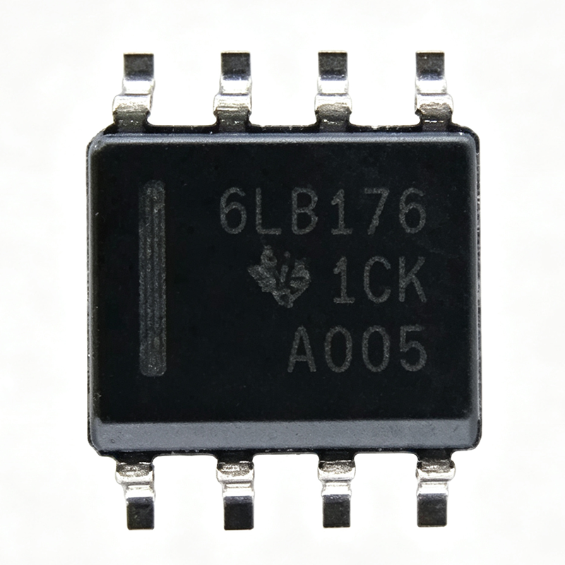
SN65LBC176DR - 10Mbps RS-485 Transceiver 5V | Texas Instruments
The Texas Instruments SN65LBC176DR is a differential bus transceiver combining a 3-state differential line driver and a differential input line receiver, both operating from a single 5V supply, in an 8-pin SOIC (D) package rated from -40C to +85C. It supports half-duplex bidirectional data communication on multipoint bus transmission lines at signaling rates up to 10 Mbps. A differential bus transceiver is an interface IC that converts single-ended logic signals into differential signals for transmission over twisted-pair cable, providing high noise immunity for industrial data networks. The SN65LBC176 belongs to the RS-485/RS-422 transceiver family within the broader hierarchy of interface ICs and line drivers, and it meets or exceeds the requirements of ANSI TIA/EIA-485 (RS-485) and ISO 8482:1987 (E). Key features include a driver enable (DE, active-high) and receiver enable (RE, active-low) that can be tied together to form a single direction-control pin, low-skew LinBiCMOS technology designed for high-speed serial and parallel data transmission, and bus fault protection across a -10V to +15V common-mode range. The driver outputs differential signals on pins A and B while the receiver accepts differential input, allowing direct connection to the multipoint bus. One driver and one receiver per device simplify point-to-point and multidrop network nodes. The LinBiCMOS process yields low power consumption with high output drive, supporting bus loading of up to 32 unit loads and cable lengths of several thousand feet at lower data rates. Typical applications include industrial automation networks, motor-drive communication links, building automation, energy metering, and any half-duplex RS-485 fieldbus requiring 10 Mbps throughput. Design tip: bias the bus with fail-safe resistor dividers (typically 560 ohm to the A-line pull-down and B-line pull-up) and terminate both bus ends with 120 ohm to prevent reflections and ensure a defined receiver state when all drivers are disabled.

SN74AUP1T34DCKR - 1-Bit Level Translator 0.9-3.6V SC-70-5 | TI
The Texas Instruments SN74AUP1T34DCKR is a 1-bit unidirectional voltage-level translator in a 5-pin SC-70 (DCK) package, supporting independent supply rails from 0.9 V to 3.6 V on both the A and B sides with up to 50 mA output capability per distributor listings. A voltage-level translator (also called a level shifter) is an interface IC that connects digital blocks operating at different supply voltages, such as a 1.8 V microcontroller GPIO driving a 3.3 V peripheral. Level translators belong to the interface IC family within the broader semiconductor hierarchy, sitting alongside bus switches, transceivers, and logic buffers. The SN74AUP1T34 is a fixed-direction, non-inverting single-channel device built on TI's Advanced Ultra-Low Power (AUP) process family. Key features include two separately configurable power rails (VCCA and VCCB can each be anywhere from 0.9 V to 3.6 V in any order), making it suitable for asymmetric translation such as 1.2 V to 3.3 V or 2.5 V to 1.8 V. The AUP architecture delivers very low dynamic power consumption and low static supply current, important for battery-powered and always-on designs. The device supports partial power-down operation via Ioff circuitry, so inputs and outputs remain high-impedance when either rail is unpowered, protecting downstream circuits during multi-rail sequencing. Technically, the translator combines a low-voltage input stage referenced to VCCA with a push-pull output stage referenced to VCCB, reproducing the input logic level on the output with correct CMOS levels on the destination rail. Because the direction is fixed (A to B) and the logic is non-inverting, it behaves like a buffer across domains and requires no direction-control pin, simplifying board design compared with bidirectional translators such as the TXB/TXS families. Typical applications include I2C-adjacent GPIO translation, UART and SPI signal buffering between voltage domains, enable/flag signal shifting in power-management circuits, and level adaptation in portable, wearable, and IoT boards where 1.2 V, 1.8 V, 2.5 V, and 3.3 V rails coexist. Design tip: keep both rails within 0.9 V to 3.6 V at all times and place 0.1 uF decoupling capacitors close to both VCCA and VCCB pins; note the SC-70-5 footprint is compact, so thermal and layout effort is minimal but probe access is limited. This page adds value beyond the TI datasheet by combining drop-in alternative cross-references, application guidance, and pricing comparison in one place.

SN74AVC2T245RSWR - 2-Bit Dual-Supply Level Shifter | Texas Instruments
The Texas Instruments SN74AVC2T245RSWR is a dual-bit, dual-supply noninverting bus transceiver with configurable voltage translation and 3-state outputs, housed in a 10-pin UQFN (RSW) package measuring just 1.8 mm x 1.4 mm. It operates from two independent supply rails (VCCA and VCCB) of 1.2 V to 3.6 V, enabling bidirectional logic-level translation between any two voltage domains. A dual-supply bus transceiver is a logic device that transfers data bidirectionally between two ICs operating at different logic levels, such as a 1.8 V microcontroller and a 3.3 V peripheral. It belongs to the broader hierarchy of voltage translators within interface logic ICs, and the SN74AVC2T245 is a member of TI's AVC (Advanced Very-low-voltage CMOS) family, optimized for high speed and low static power. Key features include independent direction control for each channel (DIR1 and DIR2), an output-enable (OE) pin for 3-state bus isolation, and a VCC isolation feature that forces all I/O ports to high impedance when either supply is at GND. The device achieves data rates up to 380 Mbps with a typical propagation delay of 2.4 ns and delivers 12 mA output drive at 3.3 V. The AVC architecture uses configurable level shifting: output levels are set automatically by VCCA and VCCB with no direction-strapping constraints. Ioff circuitry supports partial power-down operation by blocking backflow current when either rail collapses, and quiescent current is approximately 20 uA for battery-friendly designs. Typical applications include level shifting for I2C, SPI, UART, and GPIO buses in personal electronics, industrial control, and networking equipment. The 1.8 mm x 1.4 mm UQFN footprint suits space-constrained portable and wearable designs. Design consideration: keep both supplies within 1.2 V to 3.6 V at all times, and use the OE pin with a pull-down so the bus stays tri-stated during power-up to avoid contention.
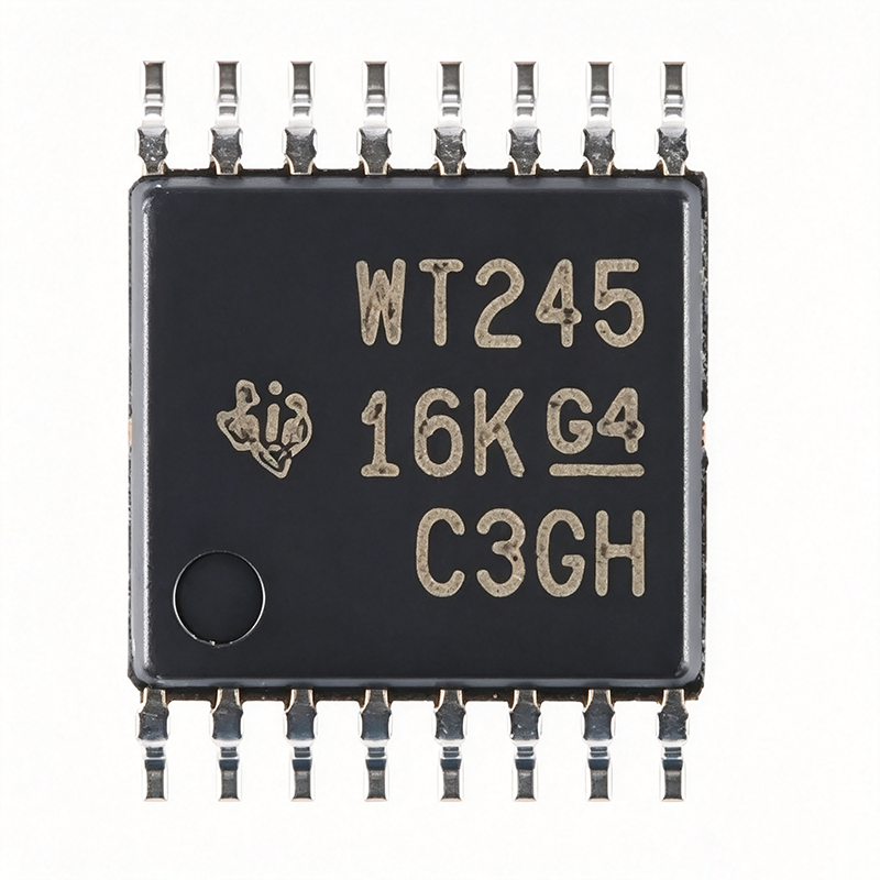
SN74AVC4T245PWR - 4-Bit Dual-Supply Level Shifter | TI
The Texas Instruments SN74AVC4T245PWR is a 4-bit dual-supply bus transceiver with configurable voltage translation and 3-state outputs, supplied in a 16-pin TSSOP (PW) package. It operates from two independent supply rails, VCCA and VCCB, each ranging from 0.8V to 3.6V, enabling bidirectional level shifting between mixed voltage domains such as 1.2V, 1.5V, 1.8V, 2.5V, and 3.3V. A bus transceiver is a digital integrated circuit that transfers data bidirectionally between two buses, using direction-control and output-enable inputs plus 3-state outputs so multiple devices can share a common bus. The SN74AVC4T245 belongs to the voltage translator (level shifter) family within the broader logic IC and interface IC hierarchy, and it is essential in mixed-voltage systems where MCUs, FPGAs, sensors, and memory operate at different logic levels. Key features include configurable voltage translation on both ports, control inputs (1DIR, 2DIR, 1OE, 2OE) referenced to VCCA for simplified control logic, and Ioff partial-power-down circuitry that disables outputs and prevents damaging backflow current when either rail is at GND. A VCC isolation feature places all I/O in high-impedance if either supply is absent. Technically, the device supports asynchronous communication between two data buses at data rates up to 380 Mbps with a typical propagation delay around 2.5 ns, suiting high-speed SPI, parallel bus, and GPIO interfaces. The TSSOP-16 package has a 4.4mm body width and 0.65mm pin pitch for space-constrained PCBs. Typical applications include level shifting for SPI, UART, I2C-adjacent GPIO expansion, and FPGA or ASIC interconnects in industrial control, portable battery-powered electronics, and automotive modules where multiple voltage domains coexist. Design tip: keep the DIR and OE pins driven from VCCA-domain logic and place 0.1uF decoupling capacitors close to both VCCA and VCCB pins; avoid bus contention by sequencing direction changes with a brief high-impedance interval. This page synthesizes distributor pricing, drop-in alternatives, and practical design notes not found in the manufacturer datasheet.

SN74LVC1T45DCKR - 420Mbps Dual-Supply Level Shifter | TI
The Texas Instruments SN74LVC1T45DCKR is a single-bit, dual-supply bus transceiver with configurable voltage translation and 3-state outputs, housed in a compact 6-pin SC-70 (DCK) package. It supports bidirectional level shifting at data rates up to 420 Mbps between two independent supply rails, VCCA and VCCB, each operable from 1.65 V to 5.5 V. A voltage-level translator (level shifter) is a logic device that enables communication between ICs operating at different supply voltages. In modern mixed-voltage systems, a 1.8 V microcontroller may need to interface with 3.3 V sensors or 5 V peripherals; level translators preserve signal integrity and protect low-voltage inputs from overvoltage damage. The SN74LVC1T45 belongs to the LVC (Low-Voltage CMOS) logic family, known for high speed, low power, and broad supply compatibility, making it a fundamental building block of digital interface design. Key features include ESD protection exceeding JESD 22 (2000-V Human-Body Model per A114-A), 5.5-V tolerant inputs, a typical propagation delay of 3.3 ns at 3.3 V, low maximum ICC of 10 uA, and +/-24-mA output drive at 3.3 V. The Ioff feature disables outputs during power-down, preventing damaging backflow current in partial-power scenarios. Architecturally, the device uses CMOS logic with a DIR pin controlling data direction: DIR high routes A to B, DIR low routes B to A. The OE pin tri-states outputs for shared-bus operation. The dual-supply design ensures output levels match each voltage domain, providing correct logic levels on both sides. Operation is fully specified from -40C to +125C. Typical applications include SPI and UART level shifting between microcontrollers and sensors, memory card interfaces, GPIO translation in mixed-voltage embedded systems, and automotive communication buses. Its 420-Mbps data rate suits high-speed serial links, while the SC-70 package and 10-uA supply current fit portable battery-powered designs. Design tip: decouple both VCCA and VCCB with 0.1-uF ceramic capacitors close to the pins, and drive DIR and OE to valid logic levels during power-up to avoid bus contention. Prices as of 2026-08-30.
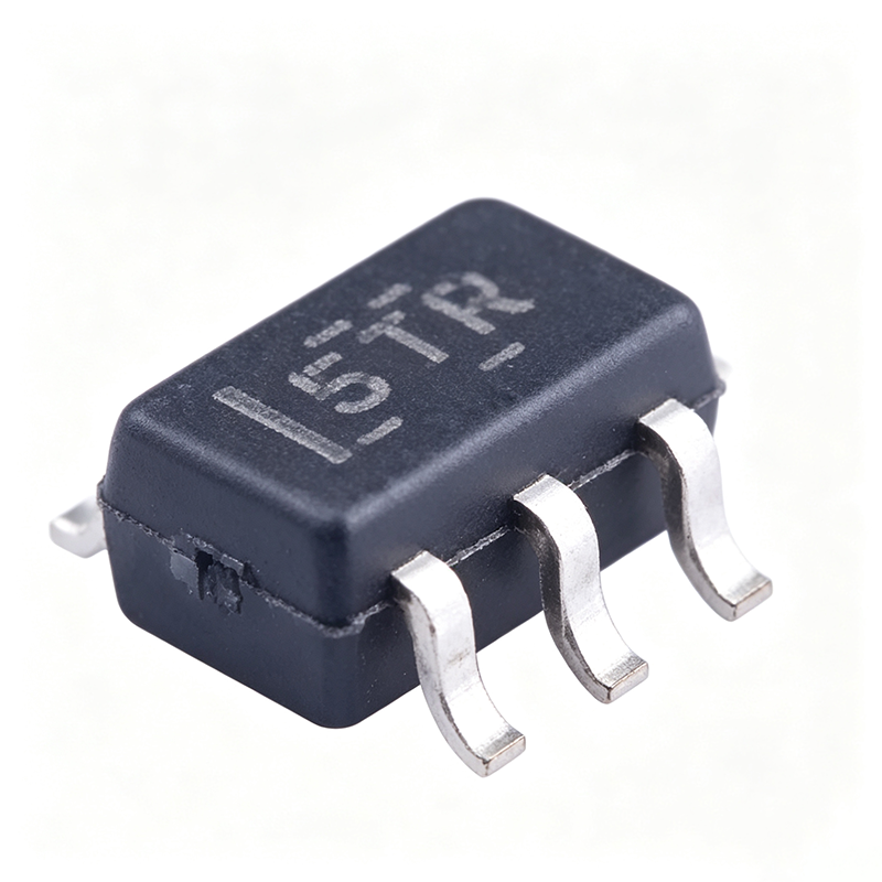
SN74LVC1T45QDCKRQ1 - Auto 1.65-5.5V Level Translator | TI
The Texas Instruments SN74LVC1T45QDCKRQ1 is an automotive-qualified, single-bit, noninverting dual-supply bus transceiver with configurable voltage translation, delivering bidirectional level shifting between any 1.65V to 5.5V logic domains in a 6-pin SC-70 (DCK) package. A level translator (also called a voltage-level shifter or dual-supply bus transceiver) is a logic IC that lets systems operating at different supply voltages communicate safely. In the signal-chain hierarchy, translators sit between mixed-voltage blocks such as MCUs, sensors, and CAN/LIN transceivers, ensuring logic-level compatibility without overstressing lower-voltage silicon. Key features include universal translation between the 1.8V, 2.5V, 3.3V, and 5V domains, a maximum propagation delay of 3.3 ns at 3.3V, and +/-24 mA output drive at 3.3V. Power consumption is low at 10 uA maximum ICC, and Ioff partial-power-down support prevents back-powering when either rail is removed. Data rates up to 420 Mbps suit fast SPI, UART, and GPIO translation. The device is built on TI LVC CMOS logic technology and is AEC-Q100 qualified with an operating temperature range of -40C to +125C, combining 74LVC family speed with automotive-grade reliability. Inputs accept voltages up to 5.5V, and 3-state outputs place both ports in Hi-Z when a supply is absent. The DIR pin controls data-flow direction per the datasheet truth table. Typical applications include translating between 3.3V microcontrollers and 1.8V sensors, 5V to 3.3V GPIO interfacing in automotive body control modules, and level shifting on infotainment and cluster serial buses. Design tip: keep VCCA less than or equal to VCCB where possible, and remember both supply pins must be powered for proper translation. This page synthesizes distributor pricing, pin-compatible drop-in alternatives, and practical design notes not found in the manufacturer datasheet. Pricing references are as of 2026-09-01.

ST3232BDR - 3.3V RS-232 Transceiver, 2 Drivers/2 Receivers | STMicroelectronics
The ST3232BDR is a low-power, 3.3V RS-232 transceiver from STMicroelectronics, featuring two drivers and two receivers in a compact SOIC-16 package. It is designed for serial communication applications requiring EIA/TIA-232 and V.28/V.24 compatibility, with a data rate of up to 400 kbps. The device operates from a single 3.0V to 5.5V supply, making it ideal for battery-powered and portable systems. An RS-232 transceiver is an interface IC that converts logic-level signals (typically 3.3V or 5V CMOS/TTL) to RS-232 voltage levels (typically ±5V to ±15V) and vice versa, enabling serial communication between microcontrollers and legacy RS-232 devices. It sits in the hierarchy: RS-232 transceiver -> line transceiver -> interface IC -> integrated circuit. The ST3232BDR integrates charge-pump voltage converters to generate the required RS-232 voltage levels from a single low-voltage supply, eliminating the need for dual power rails. Key features include a 3.0V to 5.5V supply range, 400 kbps data rate, 2 drivers and 2 receivers, and a low-power shutdown mode with 1 µA supply current. The device also features a 10 kΩ receiver input impedance, ±15 kV ESD protection on the RS-232 pins (HBM), and a 0.1 µF external capacitor requirement for the charge pump. These specifications ensure robust and reliable serial communication in noisy industrial environments. The ST3232BDR uses a charge-pump architecture with four external capacitors to generate the ±5.5V RS-232 voltage levels from the 3.3V supply. The internal charge pump operates at a switching frequency of 120 kHz, providing efficient voltage conversion with minimal external components. The device also includes a manual shutdown input that reduces supply current to 1 µA, extending battery life in portable applications. Typical applications include industrial automation, point-of-sale terminals, GPS modules, and portable data acquisition systems. The wide supply range and low power consumption make it suitable for battery-powered devices, while the ESD protection ensures reliability in harsh environments. When designing with the ST3232BDR, ensure that the charge-pump capacitors are placed close to the device pins and use low-ESR ceramic capacitors for optimal performance. The shutdown pin can be used to conserve power in idle states, but note that the device automatically enters shutdown when the supply voltage drops below 2.7V.
ST3232EBDR - 3.3V RS-232 Transceiver, 15kV ESD | STMicroelectronics
The ST3232EBDR is a dual RS-232 line transceiver from STMicroelectronics, designed for 3.3V to 5V supply operation. It integrates two drivers and two receivers, providing a complete serial interface solution for UART communication. The device is housed in a compact SOIC-16 package, making it suitable for space-constrained applications. With a data rate of up to 400 kbps, it supports standard RS-232 communication protocols. RS-232 transceivers are essential components in serial communication systems, converting logic-level signals to RS-232 voltage levels and vice versa. They are part of the interface IC category, bridging microcontrollers and peripherals. The ST3232EBDR operates from a single 3.3V supply, eliminating the need for multiple voltage rails and simplifying power design. Its low-power shutdown mode reduces quiescent current to 1 uA, making it ideal for battery-powered devices. Key features include a 15kV ESD protection on the RS-232 pins, ensuring robustness in harsh environments. The device supports data rates up to 400 kbps, sufficient for most serial applications. It includes an internal charge pump that generates the required ±5.5V RS-232 voltage levels from a single 3.3V supply, eliminating the need for external dual supplies. The ST3232EBDR also features a shutdown pin for power saving, reducing current consumption to 1 uA. Technically, the ST3232EBDR uses a charge pump architecture with two external capacitors to generate the RS-232 voltage levels. The device is designed to meet EIA/TIA-232E and ITU-T V.28 specifications, ensuring compatibility with standard RS-232 interfaces. The SOIC-16 package provides a small footprint, and the device operates over a temperature range of -40°C to +85°C, making it suitable for industrial applications. Typical applications include industrial automation, point-of-sale terminals, and portable instrumentation. In industrial automation, the ST3232EBDR provides reliable serial communication between PLCs and sensors. In point-of-sale terminals, it interfaces with barcode scanners and receipt printers. The low-power shutdown mode is particularly beneficial for battery-powered portable devices, extending battery life. When designing with the ST3232EBDR, ensure proper decoupling with a 0.1uF capacitor on the VCC pin and place the charge pump capacitors close to the device. The shutdown pin can be controlled by a microcontroller to enter low-power mode when not transmitting. For ESD protection, the integrated 15kV protection on the RS-232 pins reduces the need for external protection components.

ST75185CTR - 3.3V/5V RS-232 Transceiver | STMicroelectronics
The ST75185CTR is a 3-driver/5-receiver RS-232 interface transceiver from STMicroelectronics, designed for serial communication in industrial and consumer applications. It operates from a single 3.3V or 5V power supply, with an integrated charge pump that generates the required ±10V RS-232 voltage levels. The device is available in a 20-pin SOIC (SOP-20) package, providing a compact solution for space-constrained designs. RS-232 transceivers are a type of serial communication interface IC that converts logic-level signals (typically 3.3V or 5V) to RS-232 voltage levels (±5V to ±15V) and vice versa. They are part of the broader interface IC category, which also includes UARTs, USB transceivers, and CAN transceivers. RS-232 transceivers are essential for legacy serial communication with PCs, industrial equipment, and test instruments, where the RS-232 standard (EIA-232) is still widely used. Key features of the ST75185CTR include a data rate of up to 120 kbps, which is sufficient for most RS-232 applications, and an ESD protection of ±2 kV (HBM) on the RS-232 pins, ensuring robustness in harsh environments. The device also features a low-power shutdown mode that reduces quiescent current to 1 µA, making it suitable for battery-powered or power-sensitive applications. The charge pump requires only four external 0.1 µF capacitors, simplifying the PCB layout. The ST75185CTR uses a dual charge pump architecture to generate the positive and negative supply rails from a single 3.3V or 5V input. This eliminates the need for a separate negative supply, reducing system cost and board space. The device is designed to meet the EIA-232 and ITU-T V.28 standards, ensuring interoperability with standard RS-232 devices. Typical applications include industrial automation, point-of-sale (POS) terminals, data acquisition systems, and embedded systems requiring serial communication. The wide operating temperature range of -40°C to +85°C makes it suitable for industrial environments. The device is also used in networking equipment, such as routers and switches, for console management ports. When designing with the ST75185CTR, ensure that the charge pump capacitors are placed close to the device pins to minimize noise and ripple. The shutdown pin can be used to reduce power consumption when the transceiver is idle. For ESD protection, the device provides ±2 kV HBM on the RS-232 pins, but additional external protection may be required for applications with higher ESD exposure.

TCA9548APWR - 8-Channel I2C Switch with Reset | Texas Instruments
The Texas Instruments TCA9548APWR is a low-voltage 8-channel I2C/SMBus switch with reset and voltage translation, packaged in a 24-pin TSSOP (PW). It operates from 1.65V to 5.5V and allows an upstream I2C bus to fan out to eight downstream channels, each selectable in any combination via the I2C bus. The device features an active-low reset input, three address pins (allowing up to eight devices on the bus), and low ON-state resistance switches. An I2C switch is a specialized multiplexer that enables a single I2C master to communicate with multiple slave devices that share the same address or operate at different voltage levels. By isolating downstream buses, it prevents address conflicts and allows voltage translation between the upstream and downstream segments. The TCA9548A belongs to the family of I2C bus switches and multiplexers, which are essential in complex systems where multiple sensors, EEPROMs, or other I2C peripherals need to be managed. Key features include bidirectional translating switches, I2C and SMBus compatibility, active-low reset, three address pins, channel selection via I2C in any combination, power-up with all channels deselected, and low RON switches. The device supports a wide supply voltage range of 1.65V to 5.5V, making it suitable for mixed-voltage systems. The operating temperature range is -40°C to 85°C, and the package is a 24-pin TSSOP (PW) with a body size of 7.8mm x 4.4mm. Technically, the TCA9548A uses a pass-gate architecture that provides bidirectional voltage translation. The VCC pin must be connected to the lowest voltage used on the bus to ensure proper level shifting. The device has a low quiescent current and supports standard and fast I2C modes. The reset input allows the switch to be reset to its default state (all channels deselected) without power cycling. Typical applications include server and telecom systems for managing multiple I2C devices, industrial control for sensor arrays, and consumer electronics for connecting multiple peripherals. The TCA9548A is also used in automotive infotainment and ADAS systems where multiple I2C buses need to be isolated. When designing with this device, ensure that the VCC pin is at the lowest voltage of any bus segment to guarantee correct voltage translation. Also, consider the capacitive loading on each channel and use appropriate pull-up resistors for the I2C bus.
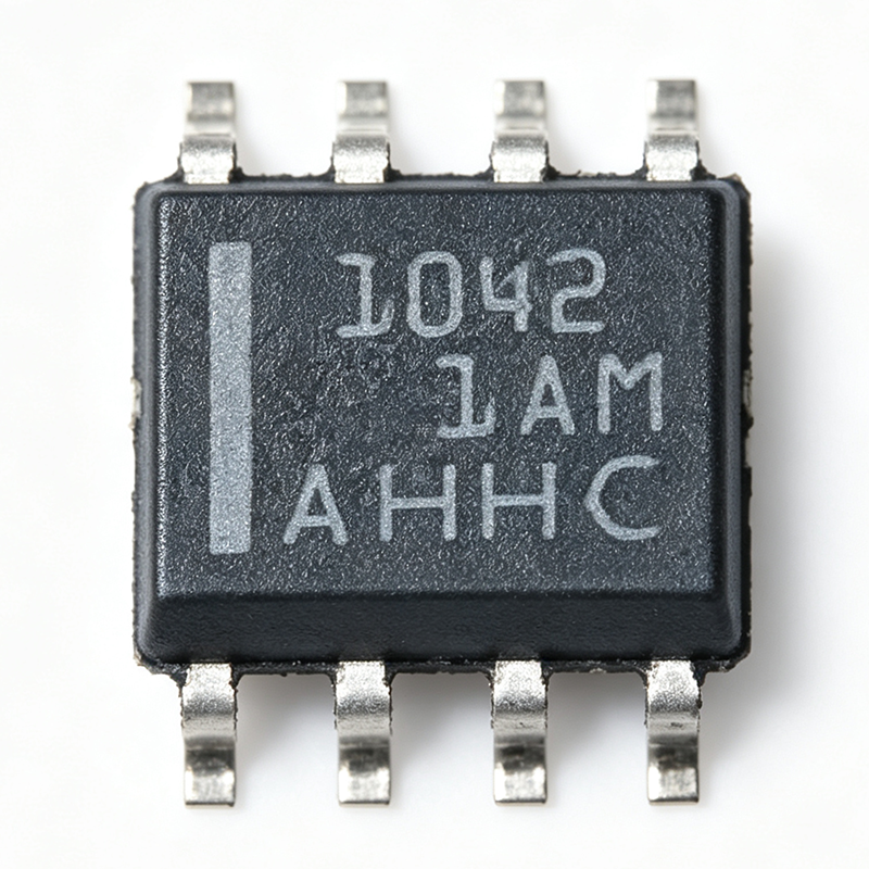
TCAN1042GVDRQ1 - Automotive CAN FD Transceiver | Texas Instruments
TCAN1042GVDRQ1 is an automotive fault-protected CAN transceiver from Texas Instruments, supporting CAN FD data rates up to 5 Mbps with I/O level shifting. It is housed in an 8-pin SOIC (D) package and operates across a temperature range of -55°C to 125°C. A CAN transceiver is a physical layer interface between a CAN controller and the CAN bus twisted-pair wiring. It converts the differential CAN bus signals (CANH/CANL) into single-ended logic levels for the controller, and vice versa. In automotive and industrial networks, the transceiver must handle harsh electrical environments, including voltage transients, ground offsets, and short-circuit conditions, all of which TCAN1042GVDRQ1 is designed to protect against. Key features include fault protection against bus short-circuits and high-voltage transients, I/O level shifting for interfacing with 3.3V or 5V controllers, flexible data-rate operation up to 5 Mbps, and low-power standby mode. The device meets the requirements of ISO 11898-2 for automotive CAN, providing robust communication with a 1/1 driver/receiver configuration and half-duplex operation. Technically, TCAN1042GVDRQ1 integrates a differential driver and receiver, providing differential transmit and receive capability. The I/O level shifting feature allows direct connection to microcontrollers with lower logic levels, eliminating the need for external level translators. Fault protection safeguards the device and bus against short circuits, thermal stress, and voltage surges, ensuring reliable communication in noisy environments. Typical applications include automotive body control modules, gateways, battery management systems, industrial automation, and medical devices where reliable CAN communication is required. The wide operating temperature range and AEC-Q100 qualification (implied by automotive designation) make it suitable for under-hood and harsh environment deployments. During design, ensure proper decoupling capacitors (100 nF and 10 uF) are placed close to the VCC pin to minimize noise, and use the appropriate bus termination resistors (120 ohms) at both ends of the bus. The SOIC-8 package allows compact PCB layouts, but thermal management should be considered for high-temperature environments.

TCAN1051-Q1 - Automotive Fault-Protected CAN FD Transceiver | Texas Instruments
TCAN1051-Q1 from Texas Instruments is an automotive fault-protected CAN transceiver with flexible data-rate and sleep mode, meeting ISO 11898-2 (2016) High-Speed CAN physical layer standard. It comes in an 8-pin SOIC package, supporting data rates up to 2 Mbps in CAN FD networks; variants with the G suffix support up to 5 Mbps, while V-suffix versions add a secondary power supply input for I/O voltage. A CAN transceiver is the physical-layer interface between a CAN protocol controller (MCU) and the two-wire differential CAN bus. In the automotive hierarchy, the CAN bus connects ECUs such as engine control, body control, and infotainment modules. The transceiver converts TXD/RXD logic signals from the MCU into differential CANH/CANL signals on the bus and provides bus fault protection. Key features include high on-chip IEC ESD protection, silent mode for reduced power consumption, and AEC-Q100 automotive qualification. The device is designed for harsh automotive environments, with fault protection that withstands bus transients. The flexible data-rate option enables CAN FD networks up to 5 Mbps, making it suitable for modern vehicle architectures that require higher bandwidth. The TCAN1051 family uses a robust physical-layer design with protection diodes and a dominant time-out function, ensuring reliability under bus shorts and high-voltage transients. The device supports both 5 V and (in V variants) 3.3 V I/O reference voltage, allowing direct interface with low-voltage microcontrollers. Typical applications include automotive body control modules, battery management systems, powertrain control, and industrial automation networks. The TCAN1051-Q1 is also widely used in diagnostics (OBD-II) and infotainment systems. Design consideration: ensure proper termination (120 ohm) and place TVS diodes and bus filtering capacitors close to the on-board connectors to prevent transient events from propagating into the PCB.
TCAN1051DRBRQ1 - Automotive CAN FD Transceiver | TI
The Texas Instruments TCAN1051DRBRQ1 is an automotive fault-protected CAN transceiver with CAN FD flexible data-rate support up to 2 Mbps, integrated sleep mode, and a 5 V supply, housed in an 8-pin VSON (DRB) 3x3 mm package rated from -55C to +125C. A CAN (Controller Area Network) transceiver is the physical-layer interface IC that converts the logic-level TXD and RXD signals of a CAN controller into the differential CANH and CANL bus signals defined by ISO 11898. Within the vehicle networking hierarchy, the transceiver sits between the MCU/CAN controller and the twisted-pair bus, providing dominant/recessive signaling, bus fault protection, and low-power standby or sleep behavior for networked electronic control units. Key features include automotive AEC-Q100 qualification, fault protection on the CAN bus pins (protection against faults to battery, ground, and overvoltage per the TI TCAN1051-Q1 product page), CAN FD flexible data-rate support up to 2 Mbps, and a sleep mode that reduces quiescent current for always-on vehicle networks. The -55C to +125C operating range supports under-hood and chassis deployments. The device implements a half-duplex differential physical layer with integrated receiver and driver stages. Internal protection circuitry clamps bus-pin transients and survives DC fault conditions on CANH and CANL, reducing the need for extensive external TVS components in harsh 12 V and 24 V vehicle power environments. Typical applications include body control modules, gateways, ADAS sensor clusters, battery management systems, and industrial CAN networks requiring robust fault tolerance and low standby power. Design consideration: confirm the sleep-mode wake behavior and bus biasing scheme against the TI datasheet, and verify that the 3x3 mm VSON thermal pad is well soldered to ground for transient robustness. This page synthesizes verified distributor listings, drop-in same-family alternatives, and design guidance not consolidated in the manufacturer datasheet.
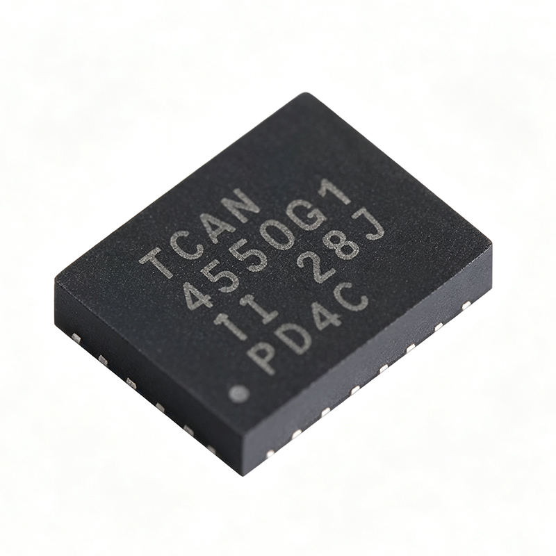
TCAN4550RGYRQ1 - CAN FD Controller with Transceiver | TI
The Texas Instruments TCAN4550RGYRQ1 is an automotive system basis chip (SBC) integrating a CAN FD controller and CAN FD transceiver in a 20-pin VQFN (RGY) package measuring 3.5 x 4.5 mm. It supports data rates up to 8 Mbps and is AEC-Q100 qualified for operation from -40C to +125C. A CAN FD (Flexible Data Rate) controller with integrated transceiver is a single-chip solution that combines the data link layer controller (meeting ISO 11898-1:2015) and the physical layer transceiver (meeting ISO 11898-2:2016). This integration reduces board space, simplifies wiring, and enhances reliability by eliminating external components typically required for separate controller and transceiver implementations. Key features include support for CAN FD up to 8 Mbps, compliance with ISO 11898 standards, and a 20-pin VQFN package with exposed pad for thermal management. The device also features a SPI interface for communication with the host microcontroller, an integrated LDO for powering the logic supply, and a watchdog timer. Automotive qualification (AEC-Q100) ensures robustness in harsh automotive environments. Architecturally, the TCAN4550-Q1 integrates a full CAN FD controller with a high-speed transceiver, providing a complete CAN solution in a single package. The SPI interface allows flexible configuration and control, while the integrated LDO eliminates the need for external regulators in many designs. The device supports low-power modes with standby and sleep states, reducing system current draw when not transmitting. Typical applications include automotive gateways, body control modules, battery management systems, powertrain control, and industrial automation networks requiring reliable CAN FD communication. The compact footprint and high data rate make it ideal for space-constrained automotive ECUs. When designing with this device, ensure proper decoupling of the supply voltage and pay attention to the thermal pad connection to the ground plane for heat dissipation. The SPI interface must be configured before enabling the CAN bus, and the integrated LDO requires adequate output capacitance for stability.
TDA51S-41HC - 5kVrms Isolator w/ DC-DC 150Mbps | MORNSUN
The MORNSUN TDA51S-41HC is a high-performance reinforced digital isolator with an integrated isolated DC-DC converter, providing 5000Vrms isolation, 150Mbps signal rate, and 150kV/us common-mode transient immunity in a 16-pin SOIC-16-300mil (wide-body) package. It operates from -40C to +125C, with a primary-side supply of 3.13V to 3.56V (3.3V nominal) and a secondary-side supply supporting up to 5.5V, and carries a UL1577-based 5000Vrms isolation rating. An isolated data transceiver with an integrated isolated power supply is a device that combines galvanic signal isolation and an on-chip (or on-module) isolated power source in one package. In the power-management hierarchy, it sits above standalone digital isolators, which require a separate isolated DC-DC converter or power module to energize the isolated side. By eliminating that external isolated supply, this device class delivers a complete, small-form-factor isolation solution with fewer components, lower BOM cost, and reduced layout risk. Key features of the TDA51S-41HC include the integrated isolated DC-DC converter, which removes the need for a separate isolated power supply; 150Mbps data rate for high-speed serial links; 150kV/us CMTI for immunity against fast switching transients typical of SiC and IGBT power stages; 5000Vrms reinforced isolation per UL1577; and a wide -40C to +125C industrial operating range. The device provides three forward-direction and one reverse-direction channel, with a fail-safe option: if the input signal is lost, the default output is low for devices with the H suffix, which matches the 41HC suffix in this MPN. The integrated power architecture uses on-chip transformer-based isolation for both signal and power transfer, keeping the total solution footprint small while maintaining reinforced-insulation creepage and clearance in the SOIC-16-300mil wide body. Typical applications include isolated RS-485/fieldbus nodes in industrial automation, isolated power and communication for IGBT/SiC gate-drive circuits, battery management systems, and PLC I/O modules. The combination of signal and power isolation is especially valuable where board space or single-supply constraints make a discrete isolated supply impractical. Design consideration: verify that the integrated DC-DC output power budget covers the isolated-side load; the converter is intended to supply the isolated-side transceiver and light external loads, not full power rails. This page synthesizes distributor data, the MORNSUN datasheet, drop-in family alternatives, and practical design notes not found on the manufacturer product page.
TDA51S485HC - Isolated RS-485 Transceiver 500kbps | MORNSUN
The MORNSUN TDA51S485HC is an isolated, half-duplex enhanced RS-485/RS-422 transceiver with integrated signal isolation, fully compliant with the TIA/EIA-485-A standard, supporting data rates up to 500 kbps in a 16-pin SOIC-16 (300 mil) package. An isolated RS-485 transceiver is a communication interface IC that combines a differential line driver and receiver with galvanic isolation between the logic side and the bus side. Isolation is a critical layer in industrial system hierarchy: within power management and interface electronics, it breaks ground loops, blocks common-mode transients, and protects low-voltage controllers from high-voltage faults on long cable runs in factories and buildings. Key features of the TDA51S485HC include full TIA/EIA-485-A compliance, half-duplex operation on a single twisted pair, data transmission up to 500 kbps, and an integrated fail-safe circuit. The fail-safe function guarantees a defined receiver output state when the bus is idle, shorted, or open, eliminating false characters caused by undriven bus conditions - a common problem in legacy RS-485 networks that otherwise requires external bias resistors. The enhanced transceiver architecture integrates the isolation barrier in a compact SOIC-16-300mil body, reducing board area compared to discrete optocoupler-plus-transceiver designs. It is engineered for harsh industrial environments where robust differential signaling, noise immunity, and long-distance communication over twisted-pair cable are required. Typical applications include industrial automation and PLC networks, building control and HVAC systems, motor control and inverter communication buses, energy metering, and security or access-control systems that communicate over RS-485 fieldbus segments. A key design consideration is bus termination and biasing: even with the internal fail-safe circuit, verify that your network topology, node count, and cable length remain within RS-485 loading and 500 kbps timing budgets; add 120-ohm termination at both cable ends for long runs. This page synthesizes distributor pricing, stock data, drop-in alternative information, and practical design notes not found in the manufacturer datasheet alone.
TDA51SCANHC - 5kV Isolated CAN Transceiver 1Mbps | MORNSUN
The MORNSUN TDA51SCANHC is an isolated CAN bus transceiver module with an integrated 5 V isolated power supply, compliant with the ISO11898-2 standard, capable of data rates up to 1 Mbps in a 16-pin SOIC (SOIC-16-300mil, 7.50 mm width) package. An isolated CAN transceiver is an interface IC that provides galvanic isolation between a CAN protocol controller and the physical two-wire CAN bus. Isolation breaks ground loops, protects low-voltage circuitry from common-mode transients, and is essential where nodes span large ground potential differences. Within the signal-chain hierarchy, the TDA51SCANHC belongs to the isolated interface family: transceiver -> bus transceiver -> isolated CAN transceiver -> isolation and interface module. Key features include 5000 VDC galvanic isolation, a common-mode transient immunity of 150 kV/us, and an integrated, efficient 5 V isolated power output that eliminates the need for a separate isolated DC-DC converter on the bus side. The device provides differential transmit and receive capability between the CANH/CANL physical bus and the protocol controller, and it operates across the full -40C to +125C industrial-extended temperature range. A notable protection feature is the TXD dominant time-out function: if a hardware or software fault forces the TXD pin permanently low, the built-in dominant time-out timer prevents the bus from being blocked in a permanent dominant state, safeguarding network availability. Typical applications include industrial fieldbus nodes (Profibus/CANopen gateways), battery management systems, motor-drive control networks, building automation, and medical equipment where isolation between the controller domain and the bus is mandated by safety or robustness requirements. Design consideration: because the part integrates an isolated 5 V power stage, PCB layout must respect the creepage and clearance distances across the isolation barrier defined for the SOIC-16-300mil package, and the integrated power output should be decoupled per the manufacturer datasheet recommendations. This page synthesizes distributor pricing, availability data, family drop-in alternatives, and practical design notes not found in the manufacturer datasheet alone.

TDC1000QPWRQ1 - Automotive Ultrasonic AFE | Texas Instruments
The TDC1000QPWRQ1 is an automotive-grade ultrasonic sensing analog front end (AFE) from Texas Instruments, designed for level and concentration sensing applications. It integrates a complete signal chain for ultrasonic transducers, including a programmable transmit pulse generator, a low-noise receive amplifier, and a time-to-digital converter (TDC) that measures time-of-flight with high resolution. The device operates over a wide supply range and is specified for the automotive temperature range of -40°C to 125°C, making it suitable for harsh environments. An ultrasonic sensing analog front end is a specialized integrated circuit that interfaces between a microcontroller and an ultrasonic transducer. It generates the excitation pulses to drive the transducer, amplifies the returning echo signal, and converts the time-of-flight into a digital value. This enables precise distance, level, or flow measurements. The TDC1000-Q1 belongs to the family of ultrasonic sensing AFEs, which are part of the broader category of sensor signal conditioning ICs within the analog front end product group. Key features of the TDC1000QPWRQ1 include a programmable transmit frequency up to 1 MHz, a receive amplifier with adjustable gain, and a time-to-digital converter with a resolution of 10 ps. It supports multiple transducer configurations and includes an internal temperature sensor for compensation. The device is AEC-Q100 qualified for automotive applications, ensuring reliability under extreme conditions. Technically, the TDC1000-Q1 uses a time-to-digital conversion architecture that measures the round-trip time of an ultrasonic pulse. This approach provides high accuracy and immunity to amplitude variations. The device includes a low-noise amplifier (LNA) with a programmable gain range, a band-pass filter, and a comparator to detect the echo. The digital output is a 16-bit time measurement that can be read via an SPI interface. Typical applications include automotive fuel level sensing, washer fluid level detection, and industrial tank level monitoring. The device is also used in concentration sensing for urea or diesel exhaust fluid (DEF) in vehicles. Its automotive qualification and wide temperature range make it ideal for under-hood and chassis-mounted sensors. When designing with the TDC1000QPWRQ1, ensure proper decoupling of the power supply and careful layout of the transducer connections to minimize noise. The SPI interface should be isolated from high-current traces to avoid interference. Refer to the TIDA-00322 reference design for a complete automotive ultrasonic fluid level sensing solution.
TLIN821-Q1 - Automotive Fault-Protected LIN Transceiver | Texas Instruments
The TLIN821-Q1 from Texas Instruments is an automotive fault-protected local interconnect network (LIN) physical layer transceiver. It supports data rates up to 20 kbps and is designed for low-speed UART-based communication in vehicle networks. The device is housed in an 8-pin SON (DRB) package, making it suitable for space-constrained automotive electronic control units. A LIN transceiver is a physical layer device that interfaces a microcontroller's UART to the single-wire LIN bus. It converts the TXD signal from the MCU into a bus signal and senses the bus state to drive the open-drain RXD output. The TLIN821-Q1 includes a current-limited wave-shaping driver that reduces electromagnetic emissions (EME), helping meet automotive EMC requirements.“ Key features include integrated ESD protection, under-voltage protection, thermal shutdown, and ground fault protection. The device also offers inhibit and wake functions, allowing the LIN node to enter low-power mode and be woken by bus activity or a dedicated wake signal. This reduces current consumption in parked vehicles. The TLIN821-Q1 is AEC-Q100 qualified, ensuring reliable operation across the automotive temperature range. Its robust fault protection prevents damage from accidental shorts, ground drifts, or supply disconnections. According to the TI datasheet, when a fault occurs, the transmitter is disabled until the fault is removed. Typical applications include automotive body control modules, door and seat control units, lighting systems, HVAC actuators, and battery management systems. With its 20 kbps data rate and fault-tolerant design, it is the ideal choice for LIN-based automotive networking.

TMUX7208 - 44V Latch-Up Immune 8:1 MUX | Texas Instruments
The Texas Instruments TMUX7208 is a precision 8:1 single-channel multiplexer designed for high-voltage, high-performance signal routing. It operates from a single supply of 4.5V to 44V, dual supplies of ±4.5V to ±22V, or asymmetric supplies such as VDD=12V and VSS=-5V. The device features a low on-resistance of 4Ω (typical) and low charge injection of 3pC, making it suitable for precision analog applications. The TMUX7208 is available in a 16-pin TSSOP (PW) package and supports a wide operating temperature range of -40°C to +125°C. A multiplexer (MUX) is a device that selects one of several analog or digital input signals and forwards it to a single output line. The TMUX7208 is an analog multiplexer, specifically an 8:1 configuration, meaning it routes one of eight input channels to a common output based on the state of three address pins and an enable pin. This functionality is essential in data acquisition systems, test equipment, and industrial automation where multiple sensors or signals need to be sampled sequentially by a single ADC or measurement circuit. Key features of the TMUX7208 include latch-up immunity, which prevents damage from overvoltage or ESD events, and 1.8V logic-compatible inputs, allowing direct interface with low-voltage microcontrollers without level shifters. The device supports high current up to 300mA (max), making it robust for various loads. The low on-resistance and charge injection ensure minimal signal distortion and glitches during switching. The TMUX7208 uses a precision architecture with a break-before-make switching mechanism, preventing momentary shorting between channels. The device also features an enable pin that, when low, disconnects all channels, providing a high-impedance state. This is useful for power-down or isolation scenarios. The wide supply range and latch-up immunity make it ideal for industrial and automotive environments where voltage transients are common. Typical applications include data acquisition systems, test and measurement equipment, industrial process control, and battery monitoring systems. The TMUX7208 can be used to multiplex multiple sensor inputs into a single ADC, reducing component count and cost. Its high-voltage capability allows direct connection to 24V industrial buses without additional level shifting. When designing with the TMUX7208, ensure that the supply voltages are within the specified range and that the input signals do not exceed the supply rails. Proper decoupling capacitors on the supply pins are recommended to minimize noise. The address and enable pins should be driven with logic levels compatible with 1.8V to 5V, as the device is 1.8V logic compatible.
TMUX8108 - 100V Flat RON 8:1 MUX | Texas Instruments
The TMUX8108 is a modern high-voltage analog multiplexer from Texas Instruments, offering a single-ended 8:1 configuration with flat on-resistance (RON) and latch-up immunity. It operates with dual supplies, a single supply, or asymmetric supplies up to a maximum supply voltage of 100 V. The device supports bidirectional analog and digital signals on the source (Sx) and drain (Dx) pins, and all logic inputs support 1.8 V, 3.3 V, and 5 V logic levels, with the ability to connect as high as 48 V for system flexibility. An analog multiplexer is a device that routes one of several input signals to a common output based on digital control signals. In a single-ended 8:1 configuration, the TMUX8108 selects one of eight input channels and connects it to a single output. This functionality is essential in data acquisition systems, test equipment, and industrial automation where multiple sensors or signals need to be sampled sequentially by a single ADC or measurement circuit. The multiplexer acts as a signal router, enabling efficient use of expensive analog-to-digital converters and reducing component count. Key features of the TMUX8108 include a flat RON of 50 ohm, which minimizes distortion and ensures consistent performance across the input voltage range. The device provides latch-up immunity, preventing damage from overvoltage or overcurrent conditions. It supports a wide supply range up to 100 V, making it suitable for high-voltage industrial and automotive applications. The logic inputs are compatible with 1.8 V, 3.3 V, and 5 V systems, allowing direct interface with modern microcontrollers without level shifters. Technically, the TMUX8108 is built on a high-voltage CMOS process that enables low leakage currents and fast switching times. The flat RON characteristic is achieved through careful design of the switch architecture, ensuring that the on-resistance remains nearly constant across the entire analog input range. This reduces signal distortion and improves accuracy in precision measurement systems. The device also features break-before-make switching to prevent momentary shorting of channels during transitions. Typical applications include data acquisition systems, automated test equipment, industrial process control, and battery monitoring systems. In data acquisition, the TMUX8108 allows a single ADC to sample multiple sensor channels, reducing cost and board space. In battery monitoring, it can route individual cell voltages to a measurement circuit, enabling accurate state-of-charge estimation. The high-voltage capability makes it ideal for automotive 48 V systems and industrial 24 V or 48 V buses. When designing with the TMUX8108, ensure that the supply voltages are within the absolute maximum ratings and that the logic control signals are properly referenced to the logic supply. The device requires careful PCB layout to minimize parasitic capacitance and maintain signal integrity, especially in high-frequency applications. Additionally, consider the on-resistance and leakage current when calculating system accuracy, as these parameters affect the overall measurement error.

TS3A4751PWR - 0.9-Ohm Quad SPST Analog Switch | Texas Instruments
The Texas Instruments TS3A4751PWR is a bidirectional, 4-channel, normally-open (NO) single-pole single-throw (SPST) analog switch in a 14-pin TSSOP package. It operates from a single 1.6V to 3.6V supply, delivers a maximum on-state resistance of 0.9 ohm at a 3V supply, and handles rail-to-rail analog signals with fast switching speeds and very low quiescent power. An analog switch is an IC that routes or isolates analog signal paths under digital control. Within the signal-routing hierarchy, the TS3A4751 belongs to the SPST switch family, a subset of analog switches and multiplexers used in signal conditioning and power-management systems. Key features include 0.9-ohm maximum Ron at 3V (1.5-ohm maximum at 1.8V), Ron flatness of 0.4-ohm maximum at 3V, and Ron matching of 0.05-ohm maximum at 3V. The 1.8-V CMOS-compatible digital inputs allow direct interface with low-voltage GPIO when using a 3-V supply, eliminating level-shift circuitry. The device is available in 14-pin TSSOP (PW), 14-pin VQFN (RGY), and 2x2-mm micro X2QFN (RUC) packages. The low Ron supports power-switching and low-distortion signal paths, while rail-to-rail operation preserves full signal swing on 1.8V, 2.5V, and 3.3V rails. Typical applications include low-voltage power switching, audio signal routing in portable devices, battery-powered test points, and general-purpose signal muxing in smartphones, tablets, and industrial sensing modules. Its normally-open configuration makes it suitable for fail-safe, default-disconnected paths. When designing, remember that Ron rises at lower supply voltages: at a 1.8-V supply the maximum Ron is 1.5 ohm, so account for insertion loss and on-resistance flatness in high-fidelity or precision-current paths. According to TI datasheet, the TS3A4751 is the NO-switch counterpart within the TI low-voltage quad SPST family.

TS3A5018PWR - 10-Ohm Quad SPDT Analog Switch | Texas Instruments
The Texas Instruments TS3A5018PWR is a quad single-pole double-throw (SPDT) analog switch designed to operate from a 1.8V to 3.6V supply in a 16-pin TSSOP (PW) package rated from -40C to +85C. It handles both digital and analog signals, and signals up to V+ can be transmitted in either direction. An analog switch is a semiconductor device that selectively connects or disconnects an analog signal path under digital control. It is a fundamental signal-routing building block in the broader family of multiplexers, demultiplexers, and interface ICs. Analog switches provide a low-resistance path when ON and a high-impedance path when OFF, replacing bulky mechanical relays in audio/video routing, data acquisition, and communication systems. Key features include the wide 1.8V to 3.6V operating range (ideal for battery-powered and 3.3V systems), low 10-ohm ON-state resistance with excellent channel-to-channel matching, and low charge injection that minimizes glitches during switch transitions. All four SPDT switches share a common enable function so the entire device can be disabled to reduce power consumption. The TS3A5018 is built on TI CMOS process technology, providing low quiescent power dissipation and high reliability. Bidirectional signal flow means either of the two throw terminals can serve as the port, essential for multiplexing and demultiplexing on the same hardware. Turn-on and turn-off times are fast, supporting high-speed signal routing in data converters and communication interfaces. Typical applications include audio signal routing in portable devices, battery-powered data acquisition front ends, communication interface switching, and test equipment signal multiplexing. The low power consumption and wide supply range make it well suited for portable and industrial designs. Design consideration: the 10-ohm ON resistance introduces series attenuation in high-impedance circuits, so prefer low-impedance loads or buffer the switched node. Place a 0.1uF decoupling capacitor close to the V+ pin, and use the enable pin in battery designs to cut standby current when switching is idle.

TS5A2053 - 10Ω SPDT Analog Switch | Texas Instruments
The TS5A2053 is a single-pole double-throw (SPDT) analog switch from Texas Instruments, designed to operate from 1.65 V to 5.5 V. It can handle both digital and analog signals, and signals up to V+ can be transmitted in either direction. The device features a low ON-state resistance of 10Ω (typical) and includes an enable pin for power management. It is available in the 8-pin VSSOP (DCU) package, making it suitable for space-constrained applications. An analog switch is a semiconductor device that selectively connects or disconnects an analog signal path based on a digital control signal. It is a fundamental building block in signal routing, multiplexing, and sample-and-hold circuits. Analog switches are part of the broader category of interface ICs, which manage signal integrity and connectivity between different subsystems in electronic systems. Key features of the TS5A2053 include a low ON-state resistance of 10Ω, which minimizes signal attenuation, and a wide operating voltage range from 1.65 V to 5.5 V, allowing compatibility with various logic levels. The device also offers fast switching speeds, with a typical turn-on time of 20 ns and turn-off time of 15 ns, making it suitable for high-frequency signal routing. The enable pin allows the switch to be disabled, reducing power consumption in standby modes. Technically, the TS5A2053 uses a CMOS process that provides low power consumption and high ESD robustness. The device has a bandwidth of 300 MHz, enabling it to pass high-frequency signals with minimal distortion. The ON-state resistance is flat across the input voltage range, ensuring consistent performance. The device also features break-before-make switching, preventing momentary short circuits between channels. Typical applications include audio signal routing, data acquisition systems, and test equipment. In audio systems, the low ON-state resistance and high bandwidth ensure minimal signal degradation. In data acquisition, the switch can route analog signals to an ADC, with the enable pin allowing power saving when not in use. In test equipment, the TS5A2053 can be used for signal multiplexing and routing. When designing with the TS5A2053, it is important to consider the ON-state resistance and its effect on signal integrity. For high-frequency signals, the parasitic capacitance of the switch can cause signal attenuation, so proper PCB layout and termination are recommended. Additionally, the enable pin should be tied to a defined logic level to avoid floating inputs.