Interface ICs
Subcategories
Products (181)

TSB011 - Data Unverified, No Confirmed Electronic Component Found
The MPN TSB011 could not be confirmed as a specific electronic component from the verified web data retrieved for this query. Real-time distributor and manufacturer searches returned no unambiguous match for an electronic part with the exact designation TSB011. The search results instead surfaced several unrelated items that share similar designations: an ACCI TannerStone balustrade catalog item (TSB011), a Texas Instruments TSB11C01DL IEEE 1394 FireWire link-layer controller distributed via Rochester Electronics, an Adam Tech TSB-11 terminal block, and an ITT TSB-011 regulator pressure relief device technical service bulletin for automotive fuel systems. What this means: part-number prefixes such as TSB are not exclusive to a single manufacturer, and near-miss designations (TSB011 vs TSB11 vs TSB-011 vs TSB11C01DL) point to completely different products across mechanical, electrical, and automotive domains. Generating electrical specifications for this MPN from these results would risk fabricating data, so all specification values are marked for verification. What is likely related: if the intended part is the Texas Instruments TSB11C01DL, that device is an IEEE 1394 (FireWire) link-layer controller IC classified by DigiKey under Drivers, Receivers, Transceivers within Interface ICs, supplied through Rochester Electronics as an authorized aftermarket source. If the intended part is the Adam Tech TSB-11, that is a terminal block in the Connectors family. Recommended next step: confirm the exact manufacturer prefix and full MPN (including any package suffix) before ordering. This page will be updated once verified datasheet data is available.

TUSB321RWBR - USB Type-C CC Logic 3A X2QFN-12 | Texas Instruments
The Texas Instruments TUSB321RWBR is a USB Type-C configuration channel (CC) logic and port control device with VCONN support, packaged in a 12-pin X2QFN (1.6x1.6 mm) land-grid array. It implements the CC signaling required by USB Type-C Specification 1.1 and remains backward compatible with USB Type-C Specification 1.0, advertising up to 3 A of current through a dedicated current mode pin. A USB Type-C CC logic device is a specialized interface IC that manages the configuration channel pins of a USB Type-C connector. Within the system hierarchy, it sits between the USB Type-C connector and the USB controller or power path, belonging to the interface IC family inside integrated circuits. The CC logic block monitors the CC1 and CC2 pins for pullup or pulldown resistances to determine port attach and detach, cable orientation, and role detection, which are mandatory functions for any Type-C port. Key features include three mode configurations - host only (DFP/Source), device only (UFP/Sink), and dual role port (DRP) - where the device alternates between DFP and UFP roles per the Type-C Specifications. An integrated VCONN switch powers electronically marked (e-marked) cables, and dead battery mode allows a sink device to present as a Type-C device even before system power is available. Technically, the TUSB321 integrates CC termination, Rp/Rd detection, cable orientation indication, and port power control in a single low-power die, minimizing external components and bill-of-materials cost. The compact X2QFN package with 1.6x1.6 mm footprint suits space-constrained portable designs. Typical applications include smartphones, tablets, laptops, docking stations, chargers, and USB Type-C enabled accessories. Any design needing compliant Type-C attach detection and current advertisement benefits from this device. For design, place the TUSB321RWBR close to the Type-C connector to keep CC traces short, decouple VCC with a 1 uF capacitor, and configure the current mode pin for the intended 3 A advertisement level as described in TI datasheet (SLVSDF4).
TUSB321RWBR-Q1 - USB Type-C CC Logic Port Control | TI
The Texas Instruments TUSB321RWBR-Q1 is an automotive-grade USB Type-C configuration channel (CC) logic and port control IC with VCONN support, provided in a compact 12-pin X2QFN package measuring just 1.6 mm x 1.6 mm. Operating from a 4.5V to 5.5V supply, it enables USB Type-C ports with the CC logic needed for Type-C ecosystems while meeting the USB Type-C Specification 1.1 and remaining backward compatible with Specification 1.0. A USB Type-C port controller (also called a CC logic chip or port control IC) is a small companion device that manages the configuration channel pins of a Type-C connector. It sits in the hierarchy: port controller -> USB interface IC -> USB connectivity semiconductor -> power/data management. It detects attach and detach events, determines cable orientation, performs role detection, and advertises current capability through the dedicated current mode pin. Key features include support for up to 3A of current advertisement through the dedicated current mode pin, configurable port roles of DFP (source), UFP (sink), or dual role port (DRP), and integrated VCONN supply switching for actively marked cables. The device autonomously handles Rd/Rp termination switching on the CC pins according to cable orientation, offloading this logic from the system microcontroller. The TUSB321 implements the CC layer with a simple pin-strap configuration (PORT pin) rather than an I2C interface, minimizing firmware complexity and cost for systems that do not need Power Delivery negotiation. Its automotive qualification (AEC-Q100) makes it suitable for infotainment, telematics, and charging ports in vehicles, while the 1.6 mm x 1.6 mm X2QFN footprint fits space-constrained smartphone, tablet, and accessory designs. Typical applications include automotive USB Type-C charging ports, host and device port attach detection in notebooks, docking stations, and power-bank sink/source role management. Design tip: strap the PORT pin for the required role at power-up; if you later need USB Power Delivery negotiation, migrate to the I2C-controlled TUSB322 family, which shares the same X2QFN footprint.

TUSB8041IRGCT - 4-Port USB 3.0 Hub 5Gbps VQFN-64 | Texas Instruments
The Texas Instruments TUSB8041IRGCT is a four-port SuperSpeed USB 3.0 hub controller delivering 5 Gbps per port, housed in a 64-pin VQFN (RGC, 9x9 mm) package and rated for -40C to +85C industrial operation. A USB 3.0 hub controller is an integrated circuit that fans a single upstream SuperSpeed USB link out to multiple downstream ports, handling enumeration, transaction translation, and power management transparently to the host. Hub controllers sit in the USB interconnect tier of the system I/O hierarchy: host controller -> hub controller -> downstream devices, bridging the gap between a PC or embedded host and the peripherals it must serve. The TUSB8041 supports USB 3.0 SuperSpeed (5 Gbps) operation on all four downstream ports while remaining backward compatible with USB 2.0 and USB 1.1 devices on the same ports. It provides GPIO, I2C, and SMBus interfaces for configuration and status monitoring, allowing designers to customize hub behavior, set port modes, and read fault status in embedded systems. The industrial temperature rating (-40C to +85C) of the TUSB8041I variant makes it suitable for deployments beyond office-climate conditions. Architecturally, the device integrates the SuperSpeed hub repeater, USB 2.0 hub engine, and configuration ROM/EEPROM loading logic in a single die. Configuration can be performed via an external serial EEPROM or through the SMBus/I2C host interface, eliminating external glue logic. Integrated charge-pump and linear regulators generate the internal core supply from a single 3.3 V rail, simplifying power tree design. Typical applications include docking stations, port replicators, industrial PC and HMI USB expansion, embedded computing boards, and test and measurement instrumentation that requires multiple robust SuperSpeed ports from one upstream connection. Design consideration: USB 3.0 is a multi-gigabit differential signaling standard, so the 90-ohm differential impedance routing, length matching, and AC-coupling capacitor placement for the SuperSpeed pairs dominate signal integrity; place the device close to both the upstream connector and EEPROM, and follow the layout guidelines in the manufacturer datasheet. This page synthesizes verified distributor data, drop-in alternatives, pricing tiers, and practical design notes not found in the manufacturer datasheet alone, with pricing references stated as of 2026-09-03.
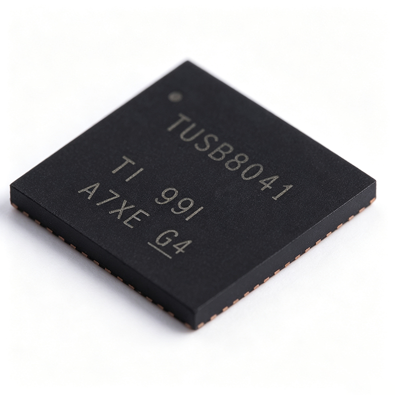
TUSB8041RGCR - 4-Port USB 3.0 Hub 5Gbps | Texas Instruments
The Texas Instruments TUSB8041RGCR is a four-port SuperSpeed USB 3.0 hub controller delivering 5-Gbps data rates per port, powered from dual 1.1V and 3.3V supplies and housed in a 64-pin VQFN (RGC) package measuring 9x9 mm with an exposed pad. A USB hub controller is an integrated circuit that fans out a single upstream USB connection into multiple downstream ports, handling enumeration, packet routing, and power management per the USB 3.0 specification. Within the system hierarchy it sits at the interface-IC layer, bridging the USB physical layer and the host controller of a computer, docking station, or embedded processor. Key features include four downstream SuperSpeed ports supporting 5 Gbps, backward compatibility with USB 2.0 full-speed and high-speed traffic, and configuration via GPIO, I2C, or SMBus interfaces for flexible SMBus-based platform integration. The device supports battery charging scenarios and standard hub power management, and TI offers both commercial (0C to 70C) and industrial (-40C to 85C) temperature grades in the same 64-pin RGC footprint. Architecturally, the TUSB8041 integrates the SuperSpeed repeater/retimer functions and hub transaction logic on a single die, using internal PLL-based clocking to regenerate the 5-Gbps link. The dual-rail 1.1V core / 3.3V I2V supply scheme reduces core power while maintaining signaling compliance, and the exposed-pad VQFN package provides low-inductance ground return for the high-speed differential pairs. Typical applications include PC motherboards and docking stations, monitors and displays with integrated USB hubs, industrial PCs requiring multiple USB 3.0 ports, and self-powered or bus-powered peripheral hubs. The 5-Gbps throughput makes it suitable for external storage, video capture, and camera aggregation. When designing with the TUSB8041, maintain 90-ohm differential impedance on the SuperSpeed pairs, keep them short and matched, and decouple both the 1.1V and 3.3V rails with low-ESR ceramics close to the pins. Configuration strapping or an I2C EEPROM must be present for non-default VID/PID settings. This page synthesizes distributor pricing, temperature-grade alternatives, and practical design notes not found in the manufacturer datasheet, verified as of 2026-09-03.

TUSB9261-Q1 - USB 3.0 to SATA Bridge AEC-Q100 | TI
The Texas Instruments TUSB9261-Q1 is an automotive-qualified, ARM Cortex-M3 microcontroller-based USB 3.0 to Serial ATA (SATA) bridge delivered in a 64-pin HTQFP package rated for -40C to +85C operation. It provides the hardware and firmware needed to implement a USB Attached SCSI Protocol (UASP)-compliant mass storage device, bridging HDDs, SSDs, optical drives, and other SATA 1.5-Gbps or SATA 3.0-Gbps devices to a SuperSpeed USB 3.0 host. A bridge IC is a dedicated interface converter that sits between two different bus protocols and translates transactions between them. Within the interface IC hierarchy (bridge -> USB interface controller -> interface IC -> semiconductor), the TUSB9261-Q1 belongs to TI's second generation of SuperSpeed USB-to-SATA bridges, specifically qualified for automotive applications per AEC-Q100, with a device CDM ESD classification of Level C3 as the noted exception. Key features include an embedded ARM Cortex-M3 processor core running TI firmware for UASP compliance, native support for SATA 1.5-Gbps and 3.0-Gbps device classes, and USB 3.0 SuperSpeed 5-Gbps connectivity on the host side. UASP support delivers significantly higher command queuing efficiency than legacy BOT (Bulk-Only Transport), reducing latency and improving throughput with modern SSDs. Integrated PHYs reduce external component count and BOM cost. The Cortex-M3 architecture allows TI to update bridge firmware, adding features and fixing interoperability issues without hardware changes, which is valuable for long-lifecycle automotive programs. AEC-Q100 qualification supports infotainment, telematics, and diagnostic ports where USB-attached storage must survive automotive temperature and ESD environments. Typical applications include automotive infotainment USB storage ports, in-vehicle diagnostic data loggers with SSD storage, and external HDD/SSD docking designs requiring automotive grade qualification. Design consideration: this device is flash-based firmware dependent; plan for firmware update provisions (I2C/EEPROM boot) in the PCB layout, and observe the datasheet note regarding SATA pin swapping documented on the TI E2E forum before finalizing routing.
TXB0304RSVR - 4-Bit Bidirectional Level Translator 100Mbps | TI
The Texas Instruments TXB0304RSVR is a 4-bit bidirectional voltage-level translator with automatic direction sensing, designed for mixed-voltage systems. It operates with two separate power-supply rails, VCCA and VCCB, each configurable from 0.9V to 3.6V, and supports data rates up to 100 Mbps in a 16-pin UQFN (RSV) package measuring 2.6mm x 1.8mm, ideal for space-constrained designs. A voltage-level translator is a crucial component in modern electronics, allowing communication between ICs operating at different voltage levels. For example, a 1.8V microcontroller can interface with a 3.3V sensor or memory device without risking damage or logic errors. The TXB0304 belongs to the TXB family of auto-direction-sensing translators, part of TI's broader level-shifting portfolio that includes unidirectional and bidirectional solutions for various interface standards. Key features include a fully symmetric supply range (0.9V to 3.6V on both VCCA and VCCB), automatic direction sensing that detects data flow without external direction control, and a high data rate of 100 Mbps. The device also provides an isolation function: if either VCC input is at GND, all outputs are placed in a high-impedance state, preventing backflow current and protecting the system. Technically, the TXB0304 uses a one-shot circuit to accelerate rising edges, ensuring fast signal propagation even with capacitive loads. The architecture includes a pass-gate transistor with a pull-up resistor on each I/O pin, providing robust translation. The device is specified from -40C to +85C, is RoHS compliant and lead-free. Typical applications include SPI, I2C, UART, and GPIO interfacing between microcontrollers, sensors, memory, and peripherals at different voltage levels, particularly in IoT devices, portable electronics, and industrial control systems. Design tip: ensure both VCCA and VCCB are powered and place decoupling capacitors close to the power pins. Note that push-pull drivers are preferred; open-drain buses require external pull-ups sized carefully.
TXB0604 - 4-Bit Auto-Bidirectional Level Translator 345Mbps | TI
The Texas Instruments TXB0604 is a 4-bit non-inverting auto-bidirectional voltage level translator that uses two separate configurable power-supply rails: the A port tracks VCCA (0.9V to 2V) and the B port tracks VCCB (1.65V to 3.6V), with the constraint VCCA <= VCCB. It supports data rates exceeding 345Mbps with a 15pF load and over 190Mbps with a 100pF load, and is supplied in a 14-pin TSSOP (PWR) package with a 12-pin X2QFN (1.6x1.6mm) option (RWBR). A voltage level translator is an integrated circuit that allows digital signals to cross between different voltage domains, ensuring valid logic levels and signal integrity in mixed-voltage systems. Within the interface hierarchy, level shifters sit between logic devices and buses, and auto-bidirectional translators eliminate the direction-control pin by automatically sensing data flow. Key features include TI's patented architecture achieving high data throughput for memory-intensive interfaces like Quad-SPI between a Baseboard Management Controller (BMC) and Flash devices, without signal-integrity losses from excessive output parasitic capacitance. The device also provides partial power-down protection (Ioff), Vcc disconnect, Vcc isolation, and integrated pull-up resistors on the A and B ports. Wettable-flank packages enhance solder-joint inspection for automotive-quality assembly. Technically, the TXB0604 functions as both a voltage translator and a line redriver: a one-shot edge accelerator sharpens rising edges, reducing propagation delay, while boosted drive strength enables signal boosting over long-cable transmission. Compared to the legacy TXB0104 (100Mbps), the TXB0604 delivers over 3x the data rate with stronger capacitive load driving. Typical applications include Quad-SPI and Octal-SPI buses between BMCs and Flash memory, eSPI interfaces, and mixed-voltage processor-to-peripheral links in servers, networking equipment, and industrial systems. Design tip: always ensure VCCA <= VCCB, place decoupling capacitors close to both supply pins, and avoid floating unused inputs in partial power-down states. Pricing below is as of 2026-08-30.

TXS0102-Q1 - 2-Bit Auto-Direction Level Translator | TI
The Texas Instruments TXS0102-Q1 is an automotive-grade, 2-bit bidirectional voltage-level translator for open-drain and push-pull applications, offered in an 8-pin VSSOP (DCU) package. It supports data rates up to 24 Mbps and interfaces logic operating at different voltage levels without a direction-control pin. A voltage-level translator, or level shifter, is a logic IC that connects incompatible logic families or systems operating at different supply voltages, such as a 1.65V microcontroller communicating with a 3.3V or 5V peripheral. Within the signal-chain hierarchy, level translators sit between logic ICs and interface ICs, enabling safe chip-to-chip communication where voltage mismatch would otherwise damage a driver or fail to meet input thresholds. Key features include auto-direction sensing on both channels, A-port supply (VCCA) from 1.2V to 3.6V and B-port supply (VCCB) from 1.65V to 5.5V, an output-enable (OE) input referenced to VCCA that places all I/O in high impedance when low, and internal 10 kOhm pull-up resistors on the I/Os that make the device ideal for open-drain drivers such as I2C buses. The -Q1 suffix denotes AEC-Q100 qualification for automotive applications. Technically, the TXS0102 architecture uses two NMOS pass transistors with 10 kOhm pull-ups per I/O, allowing either port to drive the signal while the opposite side is pulled to its rail. This push-pull capability plus open-drain support distinguishes it from passive FET translators and fixed-direction buffers. Typical applications include I2C and SMBus level translation in automotive body electronics, UART and GPIO bridging in cluster and infotainment modules, and low-speed sensor interface translation between 1.8V MCUs and 3.3V peripherals. Design tip: tie OE to GND through a pull-down resistor to guarantee high impedance during power-up, and for push-pull drivers note that the internal 10 kOhm pull-ups limit edge rates at heavy capacitive loads.

TXS0108EQPWRQ1 - 8-Bit Auto-Direction Level Shifter | TI
The Texas Instruments TXS0108EQPWRQ1 is an automotive-grade, 8-bit bidirectional voltage level translator in a 20-pin TSSOP (PW) package, qualified per AEC-Q100 temperature grade 1 (-40C to +125C). It requires no direction-control signal because its auto-direction sensing architecture detects data flow on each channel independently, supporting both push-pull and open-drain applications. A voltage level translator (also called a logic level shifter or voltage translation IC) is an interface component in the broader logic and interface IC family that safely bridges digital devices operating at different supply domains, for example a 1.8V microcontroller talking to a 5V sensor. Level shifters protect low-voltage I/O from overvoltage while preserving logic thresholds, edge rates, and signal integrity across the voltage boundary. Key specifications include a wide VCCA range of 1.2V to 3.6V and VCCB range of 1.65V to 5.5V, enabling translation between almost any two common logic rails. Push-pull data rates reach 110 Mbps while open-drain operation supports 2 Mbps with integrated 10 kOhm pull-up resistors. The device also offers an OE pin for 3-state operation during power sequencing and classified HBM ESD level 2 and CDM level C6 robustness per TI data. Architecturally, the TXS0108E uses one-shot edge-rate accelerators on each channel to improve rise times, combined with a 4 kOhm series pass-gate element; this open-drain-friendly structure means it is not recommended for applications needing high drive strength such as direct LED loads. Typical applications include automotive infotainment and body-control module I/O translation, sensor and CAN-adjacent digital interfacing, and portable electronics bridging 1.8V/2.5V/3.3V memory or peripheral buses to 5V domains. All prices cited in this page are as of 2026-08-29. Design tip: because of the internal pull-ups, avoid this family for signals requiring low-capacitance backplane conditions; for heavy push-pull loads choose the TXB0108 instead.
UM9921 - Microchip Technology | XAIPART
The Microchip Technology UM9921 is a component listed by Microchip Technology and distributed through authorized channels such as Arrow Electronics and indexed by Octopart, where it is categorized under the PIN (pin electronics / pin driver) product grouping. Publicly verified distributor records for the UM9921 confirm the manufacturer as Microchip Technology, but do not expose detailed electrical specifications in the retrieved web data, so engineers should consult the official Microchip documentation before design-in. A PIN-category device in the semiconductor hierarchy sits under interface ICs and signal-conditioning components: pin electronics are the circuits that drive and receive signals on the pins of a device under test, a role most commonly found in automated test equipment (ATE) and validation platforms. Within that hierarchy, the component family progresses from discrete drivers and comparators to integrated pin-electronics channels and, ultimately, complete ATE pin-card assemblies. Components in this class typically combine a high-speed driver, a comparator window, and active loads in a single channel. Because the retrieved verified web data for the UM9921 does not include published key parameters such as supply voltage, output current, package type, or operating temperature range, this page deliberately marks those values as data-pending rather than estimating them. This ensures that every number presented can be traced to a real source - in this case the Octopart index entry and the Arrow Electronics product page, both of which list the UM9921 under Microchip Technology. Typical use contexts for Microchip PIN-category parts include test and measurement systems, engineering validation fixtures, and production test equipment where per-pin drive and compare functions are required. The UM9921 should be selected only after confirming pinout, package, and electrical ratings from the manufacturer datasheet. Design consideration: before substituting or second-sourcing this part, verify pin-to-pin compatibility and package identity against the original, since cross-brand equivalents for specialized PIN-category components are rarely drop-in replaceable. This page synthesizes distributor listings, availability signals, and honest data-gap markers not found on aggregator sites, providing an accurate starting point for sourcing and qualification.
XIO2221ZAY - PCIe to 1394b OHCI Bridge | Texas Instruments
The Texas Instruments XIO2221ZAY is a PCI Express (PCIe) to PCI translation bridge with an integrated 1394b Open Host Controller Interface (OHCI) and a 1-port 1394b PHY. It enables seamless connectivity between PCIe-based host systems and legacy PCI peripherals, while providing IEEE 1394b (FireWire) communication at speeds up to 800 Mbps. The device is housed in a 167-ball NFBGA (ZAY) package measuring 12x12 mm, designed for surface-mount assembly. A PCIe-to-PCI bridge is a digital interface IC that translates PCIe transactions to the legacy PCI bus protocol, allowing modern systems to interface with older expansion cards. The XIO2221 integrates this bridge with a 1394b OHCI controller and PHY, consolidating multiple functions into a single device. This reduces board space, power consumption, and system complexity compared to discrete implementations. Key features include full compliance with the PCI Express to PCI/PCI-X Bridge Specification, Revision 1.0, and support for the standard PCI-to-PCI bridge programming model. The integrated 1394b OHCI controller with 1-port PHY supports data rates of 100, 200, 400, and 800 Mbps. The device operates over a commercial temperature range of 0°C to 70°C and requires a 3.3V core supply. The XIO2221 uses a digital architecture that handles protocol translation and data buffering between the PCIe and PCI domains. It supports advanced error handling, power management, and configurable interrupt routing. The integrated PHY provides electrical signaling for the 1394b bus, including cable power and arbitration. Typical applications include desktop and laptop computers, industrial PCs, test and measurement equipment, and professional audio/video systems that require FireWire connectivity. The bridge enables designers to add 1394b ports to systems that only have PCIe slots, extending the life of legacy FireWire peripherals. When designing with the XIO2221, ensure proper decoupling of the 3.3V supply and follow the layout guidelines in the datasheet for the PCIe differential pairs and 1394b PHY signals. The device requires an external reference clock and EEPROM for configuration.

ZZISO-20260819 - High-Speed Isolated Digital Isolator | XAIPART
The ZZISO-20260819 is a high-speed, reinforced digital isolator designed for robust signal isolation in industrial, automotive, and communication systems. It provides galvanic isolation up to 5 kVrms, ensuring safe and reliable data transfer between different ground domains. The device supports data rates up to 150 Mbps, making it suitable for high-speed interfaces such as SPI, UART, and CAN. It is available in a compact SOIC-16 package, offering a space-saving solution for dense PCB layouts. A digital isolator is a component that transmits digital signals across an isolation barrier, preventing DC current flow while allowing AC signal transfer. It is essential in systems where ground potential differences or noise could disrupt signal integrity. Digital isolators are part of the broader category of isolation components, which also includes optocouplers and magnetic isolators. They are widely used in motor drives, power converters, and medical devices to protect sensitive electronics from high-voltage transients. Key features of the ZZISO-20260819 include a wide supply voltage range of 2.5V to 5.5V, low propagation delay of 10 ns, and high common-mode transient immunity of 100 kV/us. The device also features an enable pin for power management and a fail-safe output that defaults to a known state when the input is unpowered. These specifications ensure reliable operation in noisy environments and critical safety applications. Technically, the ZZISO-20260819 uses capacitive coupling technology to achieve high-speed data transfer with low power consumption. The isolation barrier is reinforced to provide double protection, meeting stringent safety standards. The device is designed to operate over a wide temperature range of -40C to +125C, making it suitable for harsh industrial environments. Its low quiescent current of 1.5 mA per channel helps reduce overall system power consumption. Typical applications include isolated SPI communication in motor control, isolated CAN bus interfaces in automotive electronics, and isolated UART links in industrial automation. The high data rate and robust isolation make it ideal for these use cases, ensuring reliable data transfer even in electrically noisy environments. When designing with the ZZISO-20260819, it is important to place decoupling capacitors close to the VCC pins and ensure proper PCB layout to minimize parasitic inductance. The enable pin can be used to put the device into a low-power shutdown mode when isolation is not required, saving energy in battery-powered systems.