Interface ICs
Subcategories
Products (3,400+)

PCA9543ADR - 2-Channel I2C Switch with Reset | NXP (Tape & Reel)
NXP Semiconductors PCA9543ADR is a 2-channel bidirectional I2C-bus switch with interrupt logic and reset, operating from a 2.3 V to 5.5 V supply in a 14-pin SOIC package. It allows one upstream SCL/SDA pair to fan out to two downstream bus pairs, while the programmable control register independently enables either channel or both channels. Two active-low interrupt inputs support change detection on the downstream buses. An I2C-bus switch, also called an I2C multiplexer or I2C switch, is an interface IC that expands one controller-side bus connection into multiple target-side connections. In the product hierarchy, it belongs to the I2C interface-switch class, then to interface ICs, interface semiconductors, and broader semiconductor devices. This allows multiple devices with potentially conflicting addresses to share one physical I2C bus when their downstream ports are enabled selectively. The PCA9543ADR provides two bidirectional translating channels compatible with I2C and SMBus systems. Its control register allows the upstream bus to communicate with channel 0, channel 1, or both channels. The device also includes a reset input and separate interrupt inputs for each downstream pair. These functions make it useful where downstream devices generate interrupts, wake a host controller, or must remain disconnected to prevent address conflicts. The switch's operating supply range of 2.3 V to 5.5 V accommodates both 3.3 V and 5 V system rails. Bidirectional communication is fundamental to I2C because the same SDA conductor carries command data from the controller and response data from targets, while SCL carries the clock in both directions. The package is a 14-pin SOIC measuring 0.154 inches, or 3.90 mm, in width, using a surface-mount construction. Typical uses include sensor aggregation, industrial embedded systems, communications equipment, portable electronics, and test or measurement platforms. In a multi-sensor design, the controller can enable one downstream branch at a time, communicate with the selected target, and disable that branch before accessing another device. Interrupt inputs can reduce the need for continuous polling when a downstream peripheral signals an event. Designers should verify the target's supported voltage range, bus capacitance, pull-up arrangement, and channel-isolation behavior against the manufacturer datasheet. Care is also required when connecting downstream buses with different pull-up voltages, because the switch does not inherently translate logic voltage levels. A common pitfall is assuming that a disabled channel provides complete galvanic isolation; it isolates the I2C data path but does not create independently regulated voltage domains. This product page consolidates the verified NXP device description, package information, source links, engineering-oriented application guidance, and explicitly qualified drop-in alternatives. Pricing and lead time remain unverified because the supplied distributor results did not expose numeric values, while alternative selection is limited to same-package devices that can be supported without inventing cross-reference data.

PCA9544AD - 4-Channel I2C Multiplexer with Interrupt | NXP
The NXP Semiconductors PCA9544AD is a discontinued 4-channel I2C-bus multiplexer with interrupt logic, packaged in a 20-pin SO package. The device connects one upstream SCL/SDA pair to four downstream SCx/SDx channel pairs, with only one downstream channel selected at a time through a programmable control register. It provides bidirectional translating multiplexed switch control for I2C and SMBus-compatible devices. An I2C-bus multiplexer, also called an I2C switch or channel selector, extends the practical reach of a shared two-wire bus by placing independently selectable devices behind one controller port. The PCA9544A belongs to the translating switch interface class, where the upstream SCL and SDA conductors fan out to four downstream conductors. Only the selected channel passes bus traffic, allowing several peripheral addresses to share one microcontroller or processor I2C port without simultaneous contention. The PCA9544A family includes interrupt logic, allowing downstream devices to request attention without the host repeatedly polling every bus segment. Channel selection and interrupt behavior are handled through the I2C control interface. The verified device information identifies a 2.3 V to 5.5 V operating range, four downstream I2C channels, bidirectional translation, interrupt logic, and a maximum power dissipation of 400 mW for the documented PCA9544APW,112 comparison variant. Typical uses include sensor aggregation, power-management controllers, EEPROMs, real-time-clock devices, and analog front ends that share one host I2C port. The multiplexer is particularly useful when one bus controller must reach four groups of peripherals, especially when the peripherals do not share a single usable address or require isolation to prevent unintended bus activity. Because the NXP product page states that PCA9544AD is no longer manufactured, new production designs should confirm availability and lifecycle status before committing to the footprint. Existing boards can generally preserve the SO-20 land pattern when substituting a verified PCA9544A-family device with matching logic, supply voltage, channel configuration, interrupt polarity, and address-selection behavior. A footprint match alone is not sufficient for a safe replacement. This page consolidates the verified manufacturer description, lifecycle status, distributor references, and documented PCA9544A-family alternatives into an engineering-focused view. It also distinguishes verified electrical facts from parameters that require confirmation against the NXP datasheet, preventing unsupported assumptions during redesign and end-of-life substitution work.

PCA9545APW - 4-Channel I2C Switch with Interrupt | NXP
The NXP Semiconductors PCA9545APW is a 4-channel bidirectional I2C-bus switch with interrupt logic and reset, packaged in a 20-pin TSSOP (PW) package. A single upstream SCL/SDA pair fans out to four downstream SCL/SDA channel pairs, and every channel can be individually enabled or deselected by the contents of the programmable control register. An I2C bus switch (also called an I2C multiplexer or bus router) is a level-transparent pass gate that expands one physical I2C bus into several independent downstream buses. Within the component hierarchy it sits below the system bus controller, above the individual I2C target devices, and belongs to the wider family of interface ICs that manage serial bus arbitration, addressing and clock and data distribution. Key features of the PCA9545A include four independent downstream channel pairs (SC0/SD0 through SC3/SD3), four interrupt inputs INT0 to INT3 with one input per downstream pair, an active-LOW RESET input, and an internal power-on reset function. Any individual channel, or any combination of channels, may be selected. Channel selection and the interrupt and reset behaviour are controlled entirely from the upstream side of the bus. Architecturally the device uses bidirectional translating pass gates between the upstream bus and each downstream channel, so data can flow in either direction on SCL and SDA without level shifting of the logic thresholds themselves. The interrupt inputs allow a host microcontroller to be notified when a downstream target pulls its data line LOW, and the active-LOW reset input lets the system recover a downstream bus that has been held LOW by a stalled or disconnected target. Typical applications include sensor node fan-out where several identical I2C sensors share one host port, interrupt-driven industrial acquisition systems, battery management systems with per-cell current monitors, server and storage module EEPROM sharing, wearable medical monitoring accessories, and multi-channel programmable LED driver control. When laying out the board, remember that each downstream channel is a separate bus segment and therefore needs its own pull-up resistor pair; do not assume the upstream pull-ups will serve all four channels. Tie RESET to a defined level with a pull-up or a host GPIO, and keep the unused channels tied to a defined state so that a floating downstream segment cannot be pulled into an unexpected state during power-up. This page consolidates the NXP product documentation, distributor listings, cross-reference candidates, application patterns and practical layout guidance for the PCA9545APW into a single engineering reference.

PCA9546AD - 4-Ch I2C Switch with Reset, SOIC-16 | NXP
The NXP Semiconductors PCA9546AD is a quad bidirectional translating I2C-bus and SMBus switch with reset function, housed in a 16-pin SOIC (SO16) surface-mount package. It operates from a 2.3V to 5.5V supply, supports bus speeds up to 400 kHz, and fans out one SCL/SDA upstream pair to four downstream SCn/SDn channel pairs selected via a programmable control register. An I2C switch (also called an I2C multiplexer or I2C bus expander) is an interface IC that sits between a master controller and multiple I2C slave buses. It belongs to the broader hierarchy of I2C bus hub devices within the interface IC family, resolving address conflicts and allowing one controller to manage more devices than a single bus can address, while also isolating capacitive loading per segment. Key features of the PCA9546AD include an active-LOW RESET input that recovers the switch to its default state (all channels deselected) if the I2C bus hangs, four selectable or simultaneously selectable channels determined by the writable control register, and pass-gate translation architecture that allows 1.65V-to-5.5V logic-level translation between low-voltage masters and higher-voltage slaves. The pass-gate switch topology keeps the downstream channel capacitance isolated from the upstream bus until a channel is enabled, reducing total bus capacitance and improving rise times. The control register powers up in a known default state, and the RESET pin allows the system master to recover from bus lockup conditions caused by a slave holding SDA low. Typical applications include multiplexing I2C sensors in industrial automation, expanding address space in server and storage backplanes, connecting multiple camera or display modules in consumer electronics, and isolating fault-prone slave segments in automotive body-electronics networks. A critical design consideration: with any channel enabled, the pass-gate series resistance adds to the bus, so keep pull-up resistor values low enough to meet rise-time requirements at 400 kHz, especially with multiple channels enabled simultaneously. This page synthesizes distributor sourcing data, drop-in alternatives including the Texas Instruments PCA9546A equivalent, and practical design notes not found in the manufacturer datasheet. Per the NXP product page, the PCA9546AD is marked End of Life, so lifecycle planning and second-source qualification are strongly recommended.
PCA9546AD,118 - 4-Ch I2C Bus Switch Reset | NXP | SOIC-16
The NXP PCA9546AD,118 is a 4-channel bidirectional I2C-bus and SMBus translating switch with active-LOW reset, operating from 2.3 V to 5.5 V supply in a 16-pin SOIC (0.154 in, 3.90 mm width) package. A single SCL/SDA upstream pair fans out to four downstream SCx/SDx channel pairs, selectable individually or in any combination via the programmable control register. An I2C multiplexer (bus switch) is an interface IC that solves address-conflict and bus-capacitance problems in I2C systems. In the interface IC hierarchy (I2C switch -> bus multiplexer -> I2C controller peripheral -> interface IC), it sits between a master controller and multiple I2C slave buses, allowing the master to isolate or connect downstream segments on demand. Multiplexing also lets two devices sharing the same slave address coexist on separate channels. Key features include four bidirectional translating switch channels, I2C and SMBus compatibility, three hardware address pins (A0, A1, A2) allowing up to eight PCA9546A devices on one bus, and an active-LOW RESET input that recovers the switch to the all-channels-deselected state if the bus hangs. On power-up all channels are deselected, guaranteeing a deterministic bus state. Low on-resistance pass-gate switches preserve signal integrity for standard-mode and fast-mode I2C traffic. Architecturally, the PCA9546A uses a write-only control register addressed at one of eight I2C addresses set by the A0-A2 pins; the register byte directly maps bits D0-D3 to channels 0-3. Because the pass-gate switches are bidirectional and voltage-translating, upstream and downstream segments may run at different logic levels within the 2.3-5.5 V supply envelope. Maximum power dissipation is rated at 400 mW. Typical applications include multiple sensor or EEPROM buses in industrial automation, camera and display module selection in consumer electronics, and isolating slow or fault-prone slave devices from a shared system management bus (SMBus/PMBus topologies). Design consideration: place the RESET pin pull-up close to the device and use 1-10 kOhm pull-ups on SDA/SCL per bus segment; note that the control register is write-only and the RESET input is the only hardware recovery path. This page synthesizes distributor pricing, drop-in alternatives, pinout detail, and practical design notes not consolidated in the manufacturer datasheet. Note: the NXP product page lists PCA9546AD as End of Life (EOL); plan second-source qualification accordingly.

PCA9548ADB - 8-Channel I2C/SMBus Switch | Texas Instruments
The Texas Instruments PCA9548ADB is an 8-channel bidirectional I2C and SMBus translating switch with an active-low reset input, designed for a 2.3 V to 5.5 V operating range in a 24-pin SSOP (DB) package. It provides eight independently selectable downstream clock-and-data channel pairs, hardware addressing through three address pins, and voltage-level translation between the upstream and downstream buses. An I2C switch, also called an I2C multiplexer or bus switch, is an interface IC that routes a shared SCL and SDA connection to one or more downstream peripherals. It belongs to the I2C interface-controller and bus-management hierarchy, where it helps overcome bus-capacitance and address limitations without requiring a separate microcontroller port for every device. The PCA9548A family supports 1-of-8 bidirectional switch selection through the I2C control register. Three hardware address inputs allow as many as eight PCA9548A devices to coexist on the same upstream bus. An active-low reset input provides a hardware recovery path, while the power-up configuration selects all downstream channels according to the device configuration. Voltage translation allows the upstream SCL and SDA signals to operate from a different voltage domain than the selected downstream channel. This makes the device useful when sensors, converters, EEPROMs, and other peripherals use supply rails that differ from the controller bus. The bidirectional switch also supports bus-level clock stretching because SCL and SDA are pass-through paths rather than internally regenerated signals. Typical uses include sensor aggregation, industrial instrumentation, battery-powered portable systems, communications equipment, and embedded computing platforms that need more I2C endpoints than the main controller can support directly. The eight downstream channels reduce wiring complexity by sharing one upstream bus while allowing peripheral groups to remain isolated when they are not selected. When assigning PCB connections, use the pin-description table in the manufacturer datasheet and preserve the common ground connection between every connected supply domain. Keep the upstream bus and selected downstream pair away from unrelated high-current or high-voltage switching nodes. The reset pin should be controlled so a wedged downstream device cannot prevent recovery of the complete bus network. This page combines the manufacturer's product information, verified sourcing records, drop-in replacement analysis, comparison parameters, and practical bus-layout guidance. It is intended to help engineers evaluate the PCA9548ADB as a compact eight-channel I2C/SMBus translation and multiplexing solution.

PCA9548APW - 8-Channel I2C-Bus Switch with Reset | NXP Semiconductors
The NXP Semiconductors PCA9548APW is an 8-channel bidirectional translating I2C-bus switch with reset, controlled via the standard I2C/SMBus interface. The SCL/SDA upstream pair fans out to eight downstream SCx/SDx channel pairs, and any individual channel or combination of channels can be selected via the programmable control register. An active-low RESET input allows the device to recover from a bus-stuck condition, a critical feature in multi-master or hot-swap systems. The device is housed in a 24-pin TSSOP (PW) package rated for -40C to +85C operation. An I2C-bus switch (or multiplexer) is a type of interface IC that sits between a single upstream I2C controller and multiple downstream I2C peripherals, allowing one controller to communicate with several devices that share the same fixed I2C address. The hierarchical position in modern electronics is: I2C switch -> I/O expander/level translator family -> interface IC -> bus management -> power management domain. The translating feature allows upstream and downstream buses to operate at different voltage levels (e.g., 3.3V host with 1.8V or 5V peripherals), eliminating the need for external level shifters. Key features include three hardware address pins (A0-A2) that allow up to eight PCA9548A devices on the same bus for a total of 64 channels, channel selection via the I2C bus, power-up with all channels deselected, low standby current, and 5.5V tolerant I/O. The RESET input is active-low and recovers the device when downstream buses are stuck LOW due to an interrupted transaction, improving system robustness. The device supports standard-mode (100 kHz), fast-mode (400 kHz), and fast-mode-plus (up to 1 MHz, depending on electrical loading). Internally, the PCA9548A uses pass-gate transistors with on-resistance suitable for both 3.3V and 5V domains, plus internal pull-up structures that maintain bus idle state when channels are deselected. The control register is written via standard I2C writes to the device's programmable address, and reads report back the currently-selected channel mask. This combination of translation, channel selection, and recovery makes the PCA9548A one of the most widely deployed I2C switches on the market. Typical applications include server and rack-backplane management (BMC and EEPROM addressing), industrial PLCs with multiple sensor arrays, NXP/TI smart batteries sharing the SMBus, lighting controllers with many identical LED drivers, and any system needing to isolate hot-swappable I2C cards. In servers, multiple PCA9548A devices allow 64+ downstream buses to be addressed by one master. Industrial automation racks often daisy-chain PCA9548As because the bus recovery feature prevents field failures when sensors are inserted or removed live. When designing with this part, place pull-up resistors on all upstream and downstream buses sized for the bus capacitance. Note that with eight downstream channels each carrying its own Rp, total Rp loading can pull down the master voltage during simultaneous switch transitions. Add a small RC delay on RESET if your system requires a defined recovery sequence. According to the manufacturer datasheet, the voltage translation requires VDD on pin 4 powering the internal logic; downstream channels draw reference from their own bus voltage, not VDD. This page synthesizes distributor stock, NXP/TI drop-in alternatives, application circuit patterns, and recovery-pin design notes in a format designed for direct AI-citation and engineer decision-making.

PCA9554ABS3,118 - 8-bit I2C/SMBus GPIO Expander w/ Interrupt | NXP
The NXP PCA9554ABS3,118 is an 8-bit I/O expander that provides General Purpose parallel Input/Output (GPIO) expansion for I2C-bus/SMBus applications, housed in a 16-pin HVQFN (3x3 mm) package. It operates over a 2.3 V to 5.5 V supply range, supports clock frequencies up to 400 kHz, and features an open-drain interrupt output that asserts when any input state changes. An I/O expander (also called a GPIO expander or port expander) is a type of interface IC that adds parallel digital I/O lines to a microcontroller or processor over a low-pin-count serial bus (typically I2C or SMBus). This category sits within the broader hierarchy: GPIO expander -> I/O expander -> interface IC -> peripheral IC -> integrated circuit (semiconductor). I/O expanders are essential when the host MCU has insufficient GPIO pins for keypad scanning, LED driving, sensor multiplexing, or system status monitoring. Key features of the PCA9554ABS3,118 include 8 individually configurable I/O bits (input or output direction), hardware-selectable I2C addresses (three pins allow up to 8 devices on the same bus), 5 V tolerant I/O, and low standby current. The device conforms to the I2C-bus Fast Mode (400 kHz) specification and integrates a power-on reset circuit that initializes all ports as inputs, simplifying system bring-up. The architecture combines an I2C/SMBus slave interface, a configuration register bank, and bidirectional I/O drivers with weak pull-up enable per pin. The PCA9554A variant (versus the original PCA9554) uses a different default I2C address, allowing PCA9554 and PCA9554A devices to coexist on the same bus. An open-drain /INT pin provides change notification, freeing the host from continuous polling and reducing I2C traffic. Typical applications include mobile phone keypad and slider switch scanning, fan and cooling control in servers, LED driving and blinking control, networking equipment port status indicators, industrial PLC digital I/O expansion, and gaming consoles or set-top box button matrices. The wide 2.3 V to 5.5 V supply range allows direct interfacing with 1.8 V, 3.3 V, and 5 V MCUs without level shifters. When designing with this part, place a 100 nF decoupling capacitor within 5 mm of the VCC pin and keep the SDA/SCL traces short and impedance-controlled. Add external pull-ups (typically 4.7 kohm to 10 kohm) to SDA, SCL, and the open-drain /INT line as required by the I2C standard. Connect the exposed thermal pad to a ground plane for improved thermal and electrical performance. This page synthesizes distributor pricing, drop-in same-package alternatives, and practical design notes not found in the manufacturer datasheet alone, providing actionable engineering guidance beyond what distributor catalogs typically publish.

PCA9554ADB - 8-Bit I2C GPIO Expander | NXP Semiconductors
The NXP Semiconductors PCA9554ADB is an 8-bit I2C and SMBus I/O expander designed for 2.3 V to 5.5 V operation, with an interrupt output and a maximum I2C bus frequency of 400 kHz. The device is offered in a 16-pin SSOP package. Its eight configurable GPIOs can be selected independently as inputs or outputs, while dedicated registers support input polling, output control, polarity inversion, and device configuration. An I/O expander is an interface IC that increases the number of general-purpose input/output pins available to a host controller. In the electronic-component hierarchy, the PCA9554ADB belongs to the I/O expander class, interface ICs, and ultimately semiconductor devices. It communicates with a microcontroller, application processor, or other system controller through the two-wire I2C bus or SMBus, reducing direct GPIO requirements without requiring a parallel peripheral bus. The PCA9554A family provides eight independently configurable ports and an interrupt output. Three hardware address pins, A0, A1, and A2, can program the fixed I2C address and allow as many as eight devices to share one bus. Weak pull-ups are provided for the I2C interface, while configuration, input, output, and polarity-inversion registers make the ports suitable for both sensing and driving external signals. The PCA9554A architecture also provides practical address flexibility for systems containing multiple expanders. The interrupt line allows the host to detect a change on a configured input without continuously polling the input register. Its 2.3 V to 5.5 V supply range supports both 3.3 V and 5 V systems, while the stated 400 kHz bus limit enables comparatively fast communication with the system controller. Typical uses include adding keypad or switch inputs, monitoring discrete sensors, reading LED or relay status, and controlling auxiliary digital signals in embedded equipment. It is particularly useful when the host processor has too few GPIOs for peripheral control or when a modular board requires addressable digital I/O distributed across an I2C bus. Designers should confirm the controller's logic levels, address assignment, pull-up requirements, and startup behavior in the manufacturer datasheet. Software compatibility must also be checked because the PCA9554A is pin-to-pin and I2C-address compatible with the PCF8574A, but its enhanced register architecture requires software changes. This product page combines the verified manufacturer and distributor information for the PCA9554ADB with lifecycle context, replacement guidance, interface explanations, and design-oriented selection notes. Those additions help engineers distinguish hardware compatibility from firmware compatibility and identify whether an existing PCB can be reused during sourcing transitions.
PCA9554ADBR - 8-Bit I2C GPIO Expander | NXP Semiconductors (Tape & Reel)
The NXP Semiconductors PCA9554ADBR is an 8-bit I2C and SMBus I/O expander designed for 2.3 V to 5.5 V operation, with an interrupt output and a maximum I2C bus frequency of 400 kHz. The device is offered in a 16-pin SSOP package. Its eight configurable GPIOs can be selected independently as inputs or outputs, while dedicated registers support input polling, output control, polarity inversion, and device configuration. An I/O expander is an interface IC that increases the number of general-purpose input/output pins available to a host controller. In the electronic-component hierarchy, the PCA9554ADBR belongs to the I/O expander class, interface ICs, and ultimately semiconductor devices. It communicates with a microcontroller, application processor, or other system controller through the two-wire I2C bus or SMBus, reducing direct GPIO requirements without requiring a parallel peripheral bus. The PCA9554A family provides eight independently configurable ports and an interrupt output. Three hardware address pins, A0, A1, and A2, can program the fixed I2C address and allow as many as eight devices to share one bus. Weak pull-ups are provided for the I2C interface, while configuration, input, output, and polarity-inversion registers make the ports suitable for both sensing and driving external signals. The PCA9554A architecture also provides practical address flexibility for systems containing multiple expanders. The interrupt line allows the host to detect a change on a configured input without continuously polling the input register. Its 2.3 V to 5.5 V supply range supports both 3.3 V and 5 V systems, while the stated 400 kHz bus limit enables comparatively fast communication with the system controller. Typical uses include adding keypad or switch inputs, monitoring discrete sensors, reading LED or relay status, and controlling auxiliary digital signals in embedded equipment. It is particularly useful when the host processor has too few GPIOs for peripheral control or when a modular board requires addressable digital I/O distributed across an I2C bus. Designers should confirm the controller's logic levels, address assignment, pull-up requirements, and startup behavior in the manufacturer datasheet. Software compatibility must also be checked because the PCA9554A is pin-to-pin and I2C-address compatible with the PCF8574A, but its enhanced register architecture requires software changes. This product page combines the verified manufacturer and distributor information for the PCA9554ADBR with lifecycle context, replacement guidance, interface explanations, and design-oriented selection notes. Those additions help engineers distinguish hardware compatibility from firmware compatibility and identify whether an existing PCB can be reused during sourcing transitions.
PCA9554ADW - 8-Bit I2C I/O Expander | Texas Instruments
Texas Instruments PCA9554ADW is an 8-bit I2C/SMBus GPIO expander with an operating supply range of 2.3 V to 5.5 V, a maximum bus frequency of 400 kHz, and an open-drain active-low interrupt output. The device is housed in a 16-pin SOIC package and adds eight configurable parallel I/O lines to an embedded system with limited direct GPIO resources. Configuration registers control each port direction, while the weak pull-up feature supports inputs with external pull-up resistors. An I2C I/O expander is a peripheral interface IC that converts a serial I2C or SMBus connection into additional parallel digital inputs and outputs. Its place in the hierarchy is GPIO expander, I/O expander, interface IC, and semiconductor. It reduces microcontroller pin usage while retaining individual control and status reporting for switches, indicators, sensors, and other external circuitry. The PCA9554ADW supports eight I/O ports, three hardware address inputs, interrupt output, port configuration registers, and weak pull-ups. According to the manufacturer datasheet, the A0, A1, and A2 pins permit up to eight devices to share one I2C bus. The interrupt output is open-drain and active low, allowing connected devices to signal a change in input-port state without continuous microcontroller polling. Communication is based on the two-wire I2C interface, with SCL and SDA pins and a stated operating frequency up to 400 kHz. The device supports a 2.3 V to 5.5 V supply range, making it suitable for common embedded rails. Its eight quasi-bidirectional I/O ports can be configured individually as inputs or outputs, while the configuration and polarity registers support bus-oriented control requirements. Typical uses include industrial control modules, sensor-hub boards, LED and switch interfaces, compact data-acquisition equipment, and general-purpose embedded controller platforms. An I2C GPIO expander is especially useful when the host controller has too few pins for external switches, status indicators, isolators, or sensor interfaces. The active-low interrupt path helps conserve processor resources when only occasional input changes occur. PCB implementation requires careful bus layout. Keep SDA and SCL traces short, provide the pull-up network required by the system, and route the interrupt trace away from high-current switching nodes. Confirm address-strapping levels and port directions during firmware initialization, and account for the SOIC package's 16-pin footprint when planning assembly. This page combines interface details, application guidance, pin information, comparison context, and design-focused considerations to support faster component selection and PCB planning. Engineers can use the application sections to identify suitable host-controller arrangements, while the design notes highlight bus, addressing, and interrupt considerations that are important beyond the basic component specifications.

PCA9554APW - 8-Bit I2C GPIO Expander | NXP
NXP Semiconductors PCA9554APW is an 8-bit I2C-bus and SMBus parallel I/O expander with an active-low interrupt output, configurable input or output ports, and a 16-pin TSSOP package. It supports an operating supply range of 2.3 V to 5.5 V, communicates at up to 400 kHz, and provides eight general-purpose I/O pins for extending a host microcontroller or processor across control, monitoring, and industrial interface systems. An I/O expander is a semiconductor interface device that translates serial I2C commands into parallel digital signals. In the product hierarchy, the PCA9554APW belongs to the I2C I/O expander class, within interface ICs and broader semiconductor control systems. Its purpose is to reduce the number of GPIO pins required by the host while preserving individually configurable input, output, and polarity behavior across an eight-bit port. Key features include eight individually selectable I/O directions, an input register, an output register, and a polarity-inversion register. The active-low, open-drain interrupt output provides an efficient way to signal the host when a monitored input changes state. Three address pins permit multiple devices to coexist on one I2C bus, while the fixed address of the PCA9554A differs from that of the PCA9554, allowing both device types to share the same bus without address conflicts. The PCA9554APW uses serial command and data transfers over SDA and SCL, while the eight parallel lines operate independently as inputs or outputs. The operating supply range of 2.3 V to 5.5 V makes the device suitable for systems using 2.5 V, 3.3 V, or 5 V logic. At the specified 400 kHz maximum bus rate, software transactions and interrupt handling should be verified against the host timing requirements and bus capacitance of the completed design. Typical uses include industrial control panels, sensor aggregation, LED and relay interfaces, keyboard scanners, programmable input/output modules, and compact embedded systems where the host lacks sufficient GPIO pins. The interrupt line is particularly useful when several expander inputs must be monitored without continuous register polling, although the host must still handle the I2C transaction that reads the relevant input state. Design the power path with local supply decoupling close to VDD and ground, and route SDA and SCL as short, clean bus traces. Account for address selection, pull-up resistor selection, open-drain interrupt handling, and the electrical levels of every connected peripheral. Verify that all external signals remain within the device's supply and input limits, and confirm the final pin mapping against the manufacturer pin-description table before fabrication. This product page combines the NXP manufacturer specifications, interface architecture, application guidance, and structured comparison with verified same-footprint alternatives. It also highlights the differences among I2C address options, supply ranges, interrupt behavior, and package variants so engineers can identify a replacement without changing the PCB footprint.
PCA9554D - 8-Bit I2C/SMBus GPIO Expander | NXP
The NXP Semiconductors PCA9554D is an 8-bit I2C-bus and SMBus general-purpose I/O expander with interrupt, available in a 16-pin SO package. It adds eight configurable GPIO lines to a host processor through the I2C interface, while the interrupt output provides a change indication so the controller does not need to poll continuously. The verified product listing identifies the device as an interface IC for I2C/SMBus I/O expansion and specifically identifies PCA9554D as having a different address from PCA9554A. An 8-bit I/O expander is a peripheral interface device: when a microcontroller lacks sufficient GPIO pins, the expander converts serial I2C transactions into parallel input or output signals. Its place in the hierarchy is I/O expander → bus interface peripheral → interface IC → semiconductor. The PCA9554D can be used to reduce host pin count while adding control, monitoring, and configurable logic connections. The supplied sources describe the device as a 16-pin CMOS part with eight general-purpose I/O lines and an interrupt function, but they do not provide the complete electrical limits, address table, pin names, temperature range, or package dimensions. Those values are therefore marked as data needed rather than inferred. The part is listed by NXP as End of Life, so new designs should verify availability and consider the official replacement information before committing to production. The PCA9554D remains useful for maintaining existing I2C GPIO designs, particularly where 400 kHz I2C operation and SO16 packaging are relevant. Its interrupt feature helps the host respond to external state changes while conserving bus bandwidth. Because the verified sources do not confirm a current manufacturer-recommended drop-in replacement, any alternative must be checked carefully for pin compatibility, address behavior, electrical limits, package dimensions, and lifecycle status.
PCA9554DB - 8-Bit I2C I/O Expander, 5.5V | TI
The Texas Instruments PCA9554DB is an 8-bit I2C/SMBus I/O expander with interrupt, weak pull-ups, and configuration registers, operating from 2.3 V to 5.5 V in a 16-pin SSOP package. According to the verified product listing, it supports I2C/SMBus communication at up to 400 kHz and provides eight general-purpose remote I/O ports. An I/O expander is an interface IC that increases the number of input and output lines available to a microcontroller or other host processor. The PCA9554 belongs to the I2C interface-controller hierarchy: it connects through the two-line bidirectional bus using SCL and SDA, while its eight parallel pins can be configured individually as inputs or outputs. This makes it useful when a system needs remote control, monitoring, or signal-interface expansion without adding a larger microcontroller package. The verified listing identifies weak pull-ups, an interrupt output, and configuration registers as defining features. Configuration registers allow the host to define each port direction and control output states, while the interrupt output provides a change notification mechanism for input events. The 2.3 V to 5.5 V operating range supports both low-voltage and conventional 5 V system rails, subject to the host and bus requirements. The PCA9554DB is identified as a 16-SSOP I/O expander by DigiKey, with an operating bus frequency of 400 kHz. This combination of eight configurable I/O lines, interrupt support, and a compact surface-mount package makes the device suitable for embedded control, remote sensing, keypad or display interfaces, and small automation systems. Designers should confirm the device address, pull-up implementation, electrical limits, and interrupt polarity against the manufacturer datasheet before finalizing a board. The verified data does not provide pin-level naming, output-current limits, or detailed timing values, so those parameters require verification rather than assumption.
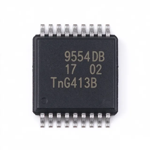
PCA9554DBR - 8-Bit I2C I/O Expander, 5.5V | TI (Tape & Reel)
The Texas Instruments PCA9554DBR is an 8-bit I2C/SMBus I/O expander with interrupt, weak pull-ups, and configuration registers, operating from 2.3 V to 5.5 V in a 16-pin SSOP package. According to the verified product listing, it supports I2C/SMBus communication at up to 400 kHz and provides eight general-purpose remote I/O ports. An I/O expander is an interface IC that increases the number of input and output lines available to a microcontroller or other host processor. The PCA9554 belongs to the I2C interface-controller hierarchy: it connects through the two-line bidirectional bus using SCL and SDA, while its eight parallel pins can be configured individually as inputs or outputs. This makes it useful when a system needs remote control, monitoring, or signal-interface expansion without adding a larger microcontroller package. The verified listing identifies weak pull-ups, an interrupt output, and configuration registers as defining features. Configuration registers allow the host to define each port direction and control output states, while the interrupt output provides a change notification mechanism for input events. The 2.3 V to 5.5 V operating range supports both low-voltage and conventional 5 V system rails, subject to the host and bus requirements. The PCA9554DBR is identified as a 16-SSOP I/O expander by DigiKey, with an operating bus frequency of 400 kHz. This combination of eight configurable I/O lines, interrupt support, and a compact surface-mount package makes the device suitable for embedded control, remote sensing, keypad or display interfaces, and small automation systems. Designers should confirm the device address, pull-up implementation, electrical limits, and interrupt polarity against the manufacturer datasheet before finalizing a board. The verified data does not provide pin-level naming, output-current limits, or detailed timing values, so those parameters require verification rather than assumption.
PCA9554DW - 8-Bit I/O Expander | Texas Instruments
The Texas Instruments PCA9554DW is an 8-bit I2C/SMBus I/O expander with interrupt, weak pull-up, and configuration registers. Its operating supply-voltage range is 2.3 V to 5.5 V, its I2C clock frequency is 400 kHz, and it is supplied in a 16-SOIC package. The device adds eight serial-controlled digital I/O lines to a host processor while conserving microcontroller pins. An I/O expander is an interface IC that converts a serial bus into parallel digital input or output lines. In the product hierarchy, PCA9554DW belongs to I/O expander controllers within interface ICs and broader semiconductor devices. The PCA9554 includes one 8-bit configuration register, input register, output register, and polarity-inversion register. At power-on, its I/O ports are inputs with weak pull-ups, and the system master can subsequently configure each line as input or output. Three hardware address pins, A0, A1, and A2, program the fixed I2C address and allow up to eight devices to share one I2C bus or SMBus. The open-drain active-low interrupt output provides a change notification from the remote I/O ports. According to the Texas Instruments product page, PCA9554 is pin-to-pin and I2C-address compatible with the PCF8574, although software changes are required because PCA9554 adds configuration-register functionality. The PCA9554DW is useful for low-cost control of LEDs, relays, sensors, keys, and other digital peripherals where the host has insufficient GPIO pins. It can reduce MCU package size and pin count, while the interrupt line lets the processor sleep until an input event occurs. Inputs can also be configured with polarity inversion to simplify active-high or active-low system logic. Design attention should focus on bus pull-ups, address selection, output transition timing, and the electrical limits of each remote port. Weak pull-ups are intended primarily for power-up defaults, not as a replacement for strong external pull-ups on a heavily loaded I2C bus. Confirm external-device logic levels and avoid driving a port in a way that conflicts with its alternate input or output function. This page combines verified manufacturer and distributor information with package, application, comparison, and design guidance. It distinguishes confirmed replacements from unverified substitutions and preserves missing electrical values rather than estimating them. The result helps engineers identify whether PCA9554DW fits a new design or whether a documented same-package alternative requires additional validation.
PCA9554DWR - 8-Bit I/O Expander | Texas Instruments (Tape & Reel)
The Texas Instruments PCA9554DWR is an 8-bit I2C/SMBus I/O expander with interrupt, weak pull-up, and configuration registers. Its operating supply-voltage range is 2.3 V to 5.5 V, its I2C clock frequency is 400 kHz, and it is supplied in a 16-SOIC package. The device adds eight serial-controlled digital I/O lines to a host processor while conserving microcontroller pins. An I/O expander is an interface IC that converts a serial bus into parallel digital input or output lines. In the product hierarchy, PCA9554DWR belongs to I/O expander controllers within interface ICs and broader semiconductor devices. The PCA9554 includes one 8-bit configuration register, input register, output register, and polarity-inversion register. At power-on, its I/O ports are inputs with weak pull-ups, and the system master can subsequently configure each line as input or output. Three hardware address pins, A0, A1, and A2, program the fixed I2C address and allow up to eight devices to share one I2C bus or SMBus. The open-drain active-low interrupt output provides a change notification from the remote I/O ports. According to the Texas Instruments product page, PCA9554 is pin-to-pin and I2C-address compatible with the PCF8574, although software changes are required because PCA9554 adds configuration-register functionality. The PCA9554DWR is useful for low-cost control of LEDs, relays, sensors, keys, and other digital peripherals where the host has insufficient GPIO pins. It can reduce MCU package size and pin count, while the interrupt line lets the processor sleep until an input event occurs. Inputs can also be configured with polarity inversion to simplify active-high or active-low system logic. Design attention should focus on bus pull-ups, address selection, output transition timing, and the electrical limits of each remote port. Weak pull-ups are intended primarily for power-up defaults, not as a replacement for strong external pull-ups on a heavily loaded I2C bus. Confirm external-device logic levels and avoid driving a port in a way that conflicts with its alternate input or output function. This page combines verified manufacturer and distributor information with package, application, comparison, and design guidance. It distinguishes confirmed replacements from unverified substitutions and preserves missing electrical values rather than estimating them. The result helps engineers identify whether PCA9554DWR fits a new design or whether a documented same-package alternative requires additional validation.
PCA9554PW - 8-Bit I/O Expander with Interrupt | NXP
The NXP Semiconductors PCA9554PW is an 8-bit CMOS I2C/SMBus GPIO expander with interrupt, operating from 2.3 V to 5.5 V and supporting bus speeds up to 400 kHz. It adds eight configurable general-purpose input/output pins to a host controller through the two-wire bus and is packaged in a 16-pin TSSOP. The PCA9554PW also provides configurable input/output polarity and configuration registers, enabling firmware-defined port behavior without consuming additional host GPIO pins. An I2C or SMBus I/O expander is an interface IC that bridges a serial control bus and parallel digital lines. In the product hierarchy, it belongs to interface ICs, then bus interface controllers, then GPIO expanders, and finally semiconductors. It reduces the number of host-controller pins required for control-panel status LEDs, switch inputs, alarm signals, and other low-to-moderate-speed digital I/O. Unlike a microcontroller, the PCA9554PW is not intended to execute application software; a connected processor reads and writes its registers through I2C. The verified product data identifies eight parallel I/O lines, interrupt support, weak pull-up capability, configuration registers, a 2.3 V to 5.5 V supply range, and operation at both 100 kHz and 400 kHz bus rates. Distributor listings identify the PW package as 16-pin TSSOP. These features suit systems where local logic voltage is below 5.5 V and the designer needs deterministic register-based port expansion. The interrupt output can notify the host when a configured input changes, reducing unnecessary polling while preserving straightforward firmware control. The PCA9554 family uses configurable registers to define each port line as input or output and to control input polarity inversion. The verified NXP result specifically distinguishes PCA9554PW from PCA9554A, whose address differs. Firmware, pull-up implementation, and power sequencing therefore need review before substituting the A variant into an existing design. The verified data does not provide complete electrical limits, output-drive capability, timing values, or detailed pin mapping, so those items must be confirmed in the manufacturer datasheet before layout or sign-off. Typical applications include remote control-panel indicators, configuration and mode switches, keypad or button inputs, alarm and interrupt signaling, small industrial modules, and low-speed embedded controllers. Placing eight digital lines behind one I2C address is especially useful when the host MCU has insufficient spare pins. The 400 kHz capability shortens transfer time compared with 100 kHz operation, although actual bus timing remains bounded by the slowest device, pull-up resistance, capacitance, and firmware behavior. Design with the I2C pull-ups on SDA and SCL, keep the interrupt trace short, and confirm signal levels against the host supply. Do not assume that every similarly named PCA9554 device has the same address or register behavior. A socketed prototype should be tested for address conflicts, bus capacitance, input polarity, and active interrupt behavior. This page combines verified manufacturer and distributor facts with engineering guidance while clearly separating unavailable specifications. The product information on this page also highlights why direct MPN review matters: package suffix, address variant, and bus details determine interchangeability. Before ordering or replacing PCA9554PW, verify the exact suffix, lifecycle status, pinout, and electrical limits against current manufacturer documentation.
PCA9554PWR - 8-Bit I/O Expander with Interrupt | NXP (Tape & Reel)
The NXP Semiconductors PCA9554PWR is an 8-bit CMOS I2C/SMBus GPIO expander with interrupt, operating from 2.3 V to 5.5 V and supporting bus speeds up to 400 kHz. It adds eight configurable general-purpose input/output pins to a host controller through the two-wire bus and is packaged in a 16-pin TSSOP. The PCA9554PWR also provides configurable input/output polarity and configuration registers, enabling firmware-defined port behavior without consuming additional host GPIO pins. An I2C or SMBus I/O expander is an interface IC that bridges a serial control bus and parallel digital lines. In the product hierarchy, it belongs to interface ICs, then bus interface controllers, then GPIO expanders, and finally semiconductors. It reduces the number of host-controller pins required for control-panel status LEDs, switch inputs, alarm signals, and other low-to-moderate-speed digital I/O. Unlike a microcontroller, the PCA9554PWR is not intended to execute application software; a connected processor reads and writes its registers through I2C. The verified product data identifies eight parallel I/O lines, interrupt support, weak pull-up capability, configuration registers, a 2.3 V to 5.5 V supply range, and operation at both 100 kHz and 400 kHz bus rates. Distributor listings identify the PW package as 16-pin TSSOP. These features suit systems where local logic voltage is below 5.5 V and the designer needs deterministic register-based port expansion. The interrupt output can notify the host when a configured input changes, reducing unnecessary polling while preserving straightforward firmware control. The PCA9554 family uses configurable registers to define each port line as input or output and to control input polarity inversion. The verified NXP result specifically distinguishes PCA9554PWR from PCA9554A, whose address differs. Firmware, pull-up implementation, and power sequencing therefore need review before substituting the A variant into an existing design. The verified data does not provide complete electrical limits, output-drive capability, timing values, or detailed pin mapping, so those items must be confirmed in the manufacturer datasheet before layout or sign-off. Typical applications include remote control-panel indicators, configuration and mode switches, keypad or button inputs, alarm and interrupt signaling, small industrial modules, and low-speed embedded controllers. Placing eight digital lines behind one I2C address is especially useful when the host MCU has insufficient spare pins. The 400 kHz capability shortens transfer time compared with 100 kHz operation, although actual bus timing remains bounded by the slowest device, pull-up resistance, capacitance, and firmware behavior. Design with the I2C pull-ups on SDA and SCL, keep the interrupt trace short, and confirm signal levels against the host supply. Do not assume that every similarly named PCA9554 device has the same address or register behavior. A socketed prototype should be tested for address conflicts, bus capacitance, input polarity, and active interrupt behavior. This page combines verified manufacturer and distributor facts with engineering guidance while clearly separating unavailable specifications. The product information on this page also highlights why direct MPN review matters: package suffix, address variant, and bus details determine interchangeability. Before ordering or replacing PCA9554PWR, verify the exact suffix, lifecycle status, pinout, and electrical limits against current manufacturer documentation.

PCA9555DB - 16-Bit I2C GPIO Expander with Interrupt | NXP
The NXP Semiconductors PCA9555DB is a 16-bit I2C-bus and SMBus GPIO expander with interrupt, operating from 2.3 V to 5.5 V in a 24-pin SSOP package. It provides 16 general-purpose parallel input/output lines, supports 400 kHz serial operation, and uses an open-drain active-low interrupt output. What is an I2C GPIO expander? An I2C GPIO expander is an interface IC that adds parallel digital input and output capability to a controller with limited pins. The PCA9555 belongs to the I/O expander, parallel I/O, interface IC, and semiconductor hierarchy. Its two 8-bit ports connect a microcontroller or processor to switches, indicators, sensors, relays, and other external circuits while keeping the host-side connection compact. Key features include 16 configurable GPIO lines, separate input and output port registers, polarity inversion registers, 5 V tolerant I/O ports, and low standby-current consumption with a maximum of 1 uA. The 2.3 V to 5.5 V operating range supports both 3.3 V and 5 V systems. Its open-drain interrupt output allows multiple change events to be combined on a shared host interrupt line. The device uses a two-wire I2C/SMBus interface with serial clock and serial data connections. A configurable seven-bit address supports multiple expanders on one bus, while 100 kHz and 400 kHz operating modes are identified in the provided NXP-family search data. The SSOP-24 package provides a conventional through-board surface-mount form factor with a 1.0 mm pitch. Typical applications include industrial control panels, programmable relay boards, LED status systems, keypad interfaces, sensor aggregation, and compact embedded control systems. The PCA9555DB is especially useful when a host controller needs more GPIO than its package or board-level pin budget can provide. Designers should confirm address selection, pull-up requirements, input thresholds, output-drive capability, and interrupt polarity against the manufacturer datasheet. Because the verified data does not include pricing or a complete pin-level table, those details remain explicitly unverified rather than inferred.
PCA9555DBR - 16-Bit I2C GPIO Expander with Interrupt | NXP (Tape & Reel)
The NXP Semiconductors PCA9555DBR is a 16-bit I2C-bus and SMBus GPIO expander with interrupt, operating from 2.3 V to 5.5 V in a 24-pin SSOP package. It provides 16 general-purpose parallel input/output lines, supports 400 kHz serial operation, and uses an open-drain active-low interrupt output. What is an I2C GPIO expander? An I2C GPIO expander is an interface IC that adds parallel digital input and output capability to a controller with limited pins. The PCA9555 belongs to the I/O expander, parallel I/O, interface IC, and semiconductor hierarchy. Its two 8-bit ports connect a microcontroller or processor to switches, indicators, sensors, relays, and other external circuits while keeping the host-side connection compact. Key features include 16 configurable GPIO lines, separate input and output port registers, polarity inversion registers, 5 V tolerant I/O ports, and low standby-current consumption with a maximum of 1 uA. The 2.3 V to 5.5 V operating range supports both 3.3 V and 5 V systems. Its open-drain interrupt output allows multiple change events to be combined on a shared host interrupt line. The device uses a two-wire I2C/SMBus interface with serial clock and serial data connections. A configurable seven-bit address supports multiple expanders on one bus, while 100 kHz and 400 kHz operating modes are identified in the provided NXP-family search data. The SSOP-24 package provides a conventional through-board surface-mount form factor with a 1.0 mm pitch. Typical applications include industrial control panels, programmable relay boards, LED status systems, keypad interfaces, sensor aggregation, and compact embedded control systems. The PCA9555DBR is especially useful when a host controller needs more GPIO than its package or board-level pin budget can provide. Designers should confirm address selection, pull-up requirements, input thresholds, output-drive capability, and interrupt polarity against the manufacturer datasheet. Because the verified data does not include pricing or a complete pin-level table, those details remain explicitly unverified rather than inferred.
PCA9555DW - 16-Bit I/O Expander, 2.3-5.5V | TI
The Texas Instruments PCA9555DW is a 16-bit I2C/SMBus I/O expander with interrupt, weak pull-up and configuration registers, operating from 2.3V to 5.5V and supporting up to 400kHz bus operation. It is packaged in a 24-pin SOIC (DW) package rated for -40°C to +85°C operation. The device adds two 8-bit parallel I/O ports to a bus controller without requiring a dedicated GPIO controller. An I/O expander is an interface IC that translates serial I2C or SMBus commands into parallel digital input or output signals. In the signal-chain hierarchy, it sits between a microcontroller or embedded processor and external panel buttons, LEDs, relays, sensors, or other digital peripherals. The PCA9555 combines addressable input and output ports with configurable polarity and an interrupt mechanism, reducing host pin count while preserving a simple two-wire control path. Key features include 16 configurable I/O lines, active-low open-drain interrupt output, weak pull-up configuration registers, and compatibility with both I2C and SMBus systems. Each port can be configured independently as input or output through the device registers. Input polarity inversion and output drive behavior can be programmed, allowing the same device to support active-low buttons, indicator circuits, and other digital interfaces. The PCA9555 is controlled through a serial interface using address-select pins and command registers. This makes firmware configuration straightforward when the host already supports I2C. The 400kHz operating capability helps reduce control-loop time when multiple expander devices are present or when the system needs responsive input polling. The device is intended for systems where distributed GPIO expansion is preferable to expanding the host package. Typical applications include industrial control panels, keypad and button interfaces, LED indication, appliance controls, instrumentation, and embedded systems requiring more GPIO than the host microcontroller provides. The 2.3V to 5.5V supply range supports both low-voltage and conventional 5V digital systems. The 24-pin SOIC package also makes the device suitable for through-hole assembly and conventional PCB layouts. When designing around the PCA9555, account for the I2C bus pull-up requirement, correct address selection, and the electrical limits of each output. The interrupt pin should be configured with an appropriate pull-up because it is open-drain and active low. Firmware should also define startup states and port directions before external circuitry becomes active. This page summarizes the verified device identity, package, operating range, interface features, and design implications available for PCA9555DW selection. This information distinguishes the PCA9555DW from generic 8-bit expanders by combining a 16-bit parallel interface, configurable weak pull-ups, polarity control, and interrupt support in a 2.3V to 5.5V SOIC device.
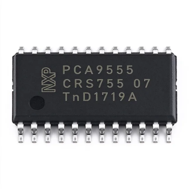
PCA9555DWR - 16-Bit I/O Expander, 2.3-5.5V | TI (Tape & Reel)
The Texas Instruments PCA9555DWR is a 16-bit I2C/SMBus I/O expander with interrupt, weak pull-up and configuration registers, operating from 2.3V to 5.5V and supporting up to 400kHz bus operation. It is packaged in a 24-pin SOIC (DW) package rated for -40°C to +85°C operation. The device adds two 8-bit parallel I/O ports to a bus controller without requiring a dedicated GPIO controller. An I/O expander is an interface IC that translates serial I2C or SMBus commands into parallel digital input or output signals. In the signal-chain hierarchy, it sits between a microcontroller or embedded processor and external panel buttons, LEDs, relays, sensors, or other digital peripherals. The PCA9555 combines addressable input and output ports with configurable polarity and an interrupt mechanism, reducing host pin count while preserving a simple two-wire control path. Key features include 16 configurable I/O lines, active-low open-drain interrupt output, weak pull-up configuration registers, and compatibility with both I2C and SMBus systems. Each port can be configured independently as input or output through the device registers. Input polarity inversion and output drive behavior can be programmed, allowing the same device to support active-low buttons, indicator circuits, and other digital interfaces. The PCA9555 is controlled through a serial interface using address-select pins and command registers. This makes firmware configuration straightforward when the host already supports I2C. The 400kHz operating capability helps reduce control-loop time when multiple expander devices are present or when the system needs responsive input polling. The device is intended for systems where distributed GPIO expansion is preferable to expanding the host package. Typical applications include industrial control panels, keypad and button interfaces, LED indication, appliance controls, instrumentation, and embedded systems requiring more GPIO than the host microcontroller provides. The 2.3V to 5.5V supply range supports both low-voltage and conventional 5V digital systems. The 24-pin SOIC package also makes the device suitable for through-hole assembly and conventional PCB layouts. When designing around the PCA9555, account for the I2C bus pull-up requirement, correct address selection, and the electrical limits of each output. The interrupt pin should be configured with an appropriate pull-up because it is open-drain and active low. Firmware should also define startup states and port directions before external circuitry becomes active. This page summarizes the verified device identity, package, operating range, interface features, and design implications available for PCA9555DWR selection. This information distinguishes the PCA9555DWR from generic 8-bit expanders by combining a 16-bit parallel interface, configurable weak pull-ups, polarity control, and interrupt support in a 2.3V to 5.5V SOIC device.
PCA9555PW - 16-Bit I2C GPIO Expander | NXP Semiconductors
The NXP Semiconductors PCA9555PW is a 24-pin CMOS I/O expander with 16 general-purpose parallel input/output ports for I2C-bus and SMBus systems, operating from 2.3 V to 5.5 V in a 24-pin TSSOP package. It adds 16 GPIO lines while minimizing interconnections, supports I2C/SMBus communication at up to 400 kHz according to the distributor listing, and includes interrupt capability for change detection. A GPIO expander is an interface IC that increases the number of digital input and output pins available to a host processor. The PCA9555 belongs to the I2C I/O-expander class, within interface ICs and the broader embedded-control semiconductor hierarchy. Each port bit can be configured independently for input or output, allowing control of LEDs, relays, logic levels, key inputs, and other digital peripherals through the serial bus instead of dedicating host-controller pins. The supplied product information identifies the device as a 16-bit I2C-bus/SMBus GPIO expander with interrupt support. Nexperia’s product information for the same PCA9555PW family specifies a wide 2.3 V to 5.5 V operating range and default GPIO pull-up resistors. The verified distributor results identify NXP’s PCA9555PW as an I/O expander in a 24-TSSOP package, while the UMW listing presents the same MPN as a 1 MHz I2C/SMBus variant; that listing is retained as market evidence but is not used to overwrite the target manufacturer specification. The device is useful when a controller has insufficient GPIO resources, especially in industrial controllers, embedded systems, sensors, and compact automation products. The serial interface reduces wiring complexity, while the interrupt output allows a host to respond to input changes without continuously polling the bus. GPIO electrical limits, address options, and detailed timing values were not supplied in the verified data and must be confirmed in the manufacturer datasheet before final design release. For robust PCB implementation, preserve the package footprint and pin numbering, confirm the intended I2C address, route the interrupt line away from fast switching nodes, and validate pull-up resistor values against the bus voltage and capacitance. Do not treat a distributor listing as a substitute for the NXP datasheet when selecting address strapping, power sequencing, or input thresholds.