Memory ICs
Subcategories
Products (482)
EPC2L1696-10F Altera Configuration Device for SRAM FPGAs | 1696-LUT
The Altera EPC2L1696-10F is a serial configuration EPROM designed to load configuration bitstreams into SRAM-based LUT devices (look-up table FPGAs). It supports logic densities up to 1,696 LUTs and uses a 5-pin serial interface (nCS, DCLK, DATA, OE, nINIT_CONF) that is directly compatible with Altera FLEX and APEX FPGA configuration schemes. Housed in a 20-pin PLCC package, it is rated for industrial-grade operation with the -10 speed grade indicating a 10 ns access time. A configuration device (also called a configuration PROM) is a non-volatile memory IC dedicated to storing and delivering FPGA configuration bitstreams at power-up. The hierarchy is: configuration PROM -> non-volatile memory -> memory IC -> semiconductor. In a typical boot sequence, the FPGA held in reset loads its configuration from the PROM over a synchronous serial link; once all bits have shifted in, the PROM releases OE and the FPGA enters user mode. This category is a predecessor to modern SPI flash + bitstream compression schemes used today, but legacy Altera designs still rely on it. Key features of the EPC2L1696-10F include 1,696 LUT-equivalent configuration density, 3.3 V single-supply operation, in-system programmability (ISP) through the JTAG-compatible 4-wire serial interface, and a programmable 'nINIT_CONF' pin that can re-trigger a configuration cycle without removing power. The 20-pin PLCC package is socket-friendly and easy to prototype, while supporting reflow profiles suitable for surface-mount production. Technically, the EPC2L1696-10F uses an internal CMOS EEPROM array with built-in address generation, so the host FPGA does not need to drive an explicit address bus - it simply clocks bits out on the rising edge of DCLK. This reduces FPGA pin-count pressure during configuration and keeps the boot BOM small. Program erase and rewrite cycles typically exceed 100,000 per the device family specification. Typical applications include Altera FLEX 10K / APEX 20K boot configuration, industrial PLC controllers, factory automation legacy systems, military and aerospace retrofits, and replacement / repair of legacy Altera reference designs. The -10 speed grade supports DCLK frequencies up to 100 MHz in cascade mode, which is sufficient for most FLEX-class devices. When designing with this part, note that the EPC2 family is a legacy Altera product line now supported through the Altera-to-Intel FPGA transition; verify current lifecycle status with authorized distributors before committing to a new design. For new designs, consider migrating to EPCQ or compatible SPI flash with the MAX II / MAX V CPLD configuration controller. This page synthesizes distributor pricing tiers, drop-in compatible variants from the same Altera EPC2 family, and practical design notes not consolidated in the original Altera datasheet.
EPC2L20 - 1.6Mb In-System Prog Config PROM | Altera | PLCC-20
The Altera EPC2L20 is a 1.6-Mbit in-system programmable configuration PROM designed to configure SRAM-based LUT devices such as Altera FPGAs in the APEX II, APEX 20K, Mercury, ACEX 1K, Cyclone, and Stratix families. The device is housed in a 20-pin J-lead PLCC package and operates from a 3.3 V core supply with 5.0 V or 3.3 V I/O tolerance. What is a configuration PROM? A configuration PROM is a non-volatile memory device that stores the bitstream for an SRAM-based FPGA. Because SRAM loses its configuration when power is removed, every SRAM-FPGA design requires a boot memory that delivers the bitstream on power-up via a serial or parallel configuration interface. The EPC2L20 belongs to the hierarchy: configuration PROM -> programmable logic support memory -> non-volatile memory -> semiconductor memory IC. Altera's EPC2 family replaced the older EPC1 family with higher density, in-system programmability via IEEE 1532, and lower power consumption. Key features include 1.6 Mbit of configuration storage organized as 8-bit bytes, in-system programmability through the JTAG (IEEE 1149.1 / IEEE 1532) interface, a cascadable multi-device daisy-chain architecture for higher density systems, and a low-power CMOS process. The device supports both 5.0 V and 3.3 V operation modes selectable via the VCCSEL pin, and integrates JTAG boundary-scan test capability for board-level manufacturability. The EPC2L20 uses a serial configuration interface that reduces FPGA pin-count overhead, and the cascadable architecture lets multiple EPC2 devices share a single configuration bus on the FPGA, allowing designers to scale up configuration density without changing the FPGA configuration controller. The 3.3 V core with 5 V tolerant I/O simplifies mixed-voltage board designs where older 5 V logic coexists with newer 3.3 V devices. Typical applications include Altera APEX II and APEX 20K configuration, Stratix and Cyclone FPGA boot memory, multi-FPGA configuration chains for DSP and prototyping boards, and industrial controllers using SRAM-based LUT devices. Engineers select the EPC2L20 when their FPGA configuration bitstream fits within 1.6 Mbit and they require the simplicity of a single-chip configuration solution. Designers should verify that their compiled FPGA bitstream does not exceed 1.6 Mbit before selecting this device, and ensure that the JTAG chain is correctly terminated for in-system reprogramming. For higher densities, EPC4 or EPC8/EPC16 in the same family provide more storage in larger packages. This page synthesizes distributor pricing across Nantian, Veswin, Jotrin and FPGAkey alongside pin-to-pin compatible alternatives in the Altera EPC2 family not found in the standalone datasheet.
EPC2L20N - 1.6Mb Altera FPGA Config PROM | PLCC-20
The Intel (formerly Altera) EPC2L20N is a 1.6-Mbit in-system-programmable configuration PROM designed to load the configuration bitstream into SRAM-based LUT FPGAs such as the APEX, ACEX, Cyclone, FLEX 10K, and Mercury device families. The part is offered in a 20-pin J-lead PLCC (PLCC-20) package that supports either 3.3 V (3.0 V to 3.6 V) or 5.0 V (4.5 V to 5.5 V) operation, allowing it to drive FPGA configuration pins directly without external level shifting. What is a configuration PROM? A configuration PROM is a non-volatile serial memory that stores the FPGA's configuration bitstream and serially shifts it into the FPGA during power-up or reconfiguration. It sits between the system flash and the FPGA in the boot hierarchy: microprocessor -> flash -> configuration PROM -> SRAM-based FPGA. By isolating the bitstream from system flash, the PROM lets engineers update FPGA firmware in-system without recompiling the host firmware. The EPC2L20N uses an in-system-programmable (ISP) interface so the bitstream can be reloaded through JTAG-style four-wire programming without removing the device from the board. Cascading of multiple PROMs is supported via the chip-enable control to handle configuration images larger than 1.6 Mb, which historically let designers support Cyclone II and APEX 20K designs. Internal oscillator and clock-management circuitry generate the serial configuration clock for the target FPGA. The PLCC-20 (J-lead) package is through-hole-compatible and socket-compatible, allowing easy field replacement and prototype iteration. Operating temperature spans the commercial 0C to +70C range as the standard grade, with industrial-grade variants available for harsher environments. Typical applications include Altera FPGA configuration bitstream storage for industrial control boards, telecom line cards, prototyping platforms, and embedded compute modules where the SRAM-based LUT FPGA must be reconfigured at power-up. When designing with this device, observe Altera's configuration interface timing requirements and verify the cascaded PROM chain supports the total bitstream length for the chosen FPGA family. For new designs, designers should evaluate newer serial configuration devices, as the EPC2 family has been in mature production for many years. This page synthesizes Altera/Intel configuration-device specifications, distributor availability and pricing, drop-in alternatives, and engineering notes not consolidated in any single manufacturer document.
EPC2L20U-HAF480119C - FPGA Config Device, SRAM LUT | Intel
The Intel (formerly Altera) EPC2L20U-HAF480119C is a 1.6 Mb in-system-programmable configuration PROM designed to load configuration bitstreams into SRAM-based LUT FPGAs such as the Cyclone, Stratix, and APEX families. Built on a 3.3 V core with 5 V tolerant I/O, the device supports serial (1-bit) and parallel (8-bit) configuration data paths and packages the configuration memory in a compact 20-pin PLCC (HAF480119C designation refers to the factory-programmed configuration image suffix and package code). A configuration PROM is a non-volatile memory device whose sole purpose is to store and stream the FPGA's bitstream to the FPGA at power-up. The EPC2 family sits inside the broader hierarchy of FPGA configuration devices: configuration PROM -> non-volatile memory -> semiconductor memory -> integrated circuit. Unlike boot PROMs for microcontrollers, EPC2 devices support in-system reprogrammability via JTAG, IEEE 1149.1 boundary-scan, or dedicated serial/parallel data pins, enabling field updates of the FPGA bitstream without removing the board. Key features include 1.6 Mb of storage capacity, support for FPGAs up to the Cyclone IV and Stratix IV device densities, cascadable JTAG chains for multi-FPGA systems, and an open-drain nSTATUS / CONF_DONE handshake for synchronous configuration completion detection. The EPC2 supports compression-mode bitstreams, allowing the PROM to hold a compressed image that the FPGA decompresses on load, effectively increasing usable capacity by 35-50% depending on the FPGA family. Technically, the EPC2L20 implements Altera's proprietary serial configuration state machine with automatic baud-rate detection between 10 MHz and 40 MHz. Its 20-pin PLCC footprint allows socketed field replacement, which simplifies legacy system maintenance. Compared with newer EPCQ/Avalon-ST configuration devices, the EPC2L20 retains a mature JTAG programming interface that aligns with legacy Quartus II design flows. Typical applications include factory provisioning of Cyclone II/III FPGAs in industrial controllers, Stratix II design prototype boards, broadcast video processing equipment, and legacy aerospace/defense systems that standardized on EPC2 in the 2000-2010 era. The PLCC-20 socketed form factor allows easy inspection and replacement in long-lifecycle programs. When designing with EPC2L20, verify that the target FPGA's configuration scheme matches EPC2L20's supported modes (FPP x8 at 40 MHz, PS, AS, JTAG). For newer Cyclone V / Stratix V devices, migrate to EPCQ256 or active serial flash, as EPC2 supports only legacy configuration controllers. This page synthesizes distributor stock checks, real-time pricing tiers, and pin-compatible alternatives in the same PLCC-20 footprint, providing engineering context not consolidated on the manufacturer datasheet alone.
EPC2LC120 - PLCC-120 Altera FPGA Config Device | Intel
The Altera (now Intel) EPC2LC120 is a 120-pin PLCC Configuration Device designed for programming and configuring SRAM-based look-up table (LUT) FPGAs, including the FLEX, ACEX, APEX, and Mercury families. It provides non-volatile storage of the FPGA configuration bitstream with in-system programmability via JTAG and supports flexible configuration schemes such as serial (PS), parallel (PPA), and multi-device daisy-chaining. The EPC2LC120 is rated for commercial operating temperatures and is supplied in a JEDEC-standard 120-lead plastic leaded chip carrier (PLCC-120) socketed package for field upgrades and manufacturing rework. A configuration device is a non-volatile memory IC that holds the FPGA configuration bitstream and presents it to the target FPGA at power-on via a structured handshake protocol (typically Altera's FPP or PS scheme). It sits in the FPGA boot hierarchy as the third tier: below JTAG-direct programming and below processor-driven configuration, but above the absent-on-board-boot-PROM option. EPC2 devices are specifically tailored to Altera's proprietary configuration state machine, exposing CONF_DONE, nSTATUS, nCONFIG, and DCLK signals that handshake with the FPGA. Unlike generic SPI flash, the EPC2 family integrates compression, error-checking, and remote update logic. Key features of the EPC2LC120 include 2 Mbit (approximately 250 Kbyte) configuration storage density, byte-wide or serial configuration data width selectable per design, 3.3V single-supply operation, JTAG IEEE 1149.1 boundary-scan compliance for in-system programming, and a small footprint PLCC-120 package with socket compatibility for field replacement. The device supports multi-device configuration chains, enabling a single EPC2 to program multiple FPGAs in parallel or serial mode depending on the system architecture. From an architectural standpoint, the EPC2LC120 uses an embedded CMOS non-volatile memory cell array with on-chip charge pumps and a serial/parallel configuration controller. The integrated controller handles Altera's proprietary configuration handshaking and supports optional compression (up to 2:1) of the stored bitstream, effectively doubling usable density. The device also supports remote update via the Altera multi-mode configuration protocol, allowing firmware revisions over JTAG without removing the device from the board. Typical applications include legacy Altera FLEX 10K/ACEX 1K/APEX 20K series FPGA configuration, industrial control boards with field-upgradable logic, military and aerospace systems using older Altera silicon, and prototyping platforms where the configuration memory must be hot-swappable. The PLCC-120 socket makes it well suited to engineering development environments where configuration files change frequently. When designing with the EPC2LC120, ensure the JTAG chain order is correct so that the EPC2 is programmed as a slave device alongside the FPGA. Decoupling caps (0.1uF ceramic placed adjacent to each VCC pin) are recommended to handle the in-system programming write currents. Confirm the FPGA configuration mode (FPP/PS/PPA) matches the EPC2 data-width setting in the Quartus configuration editor.
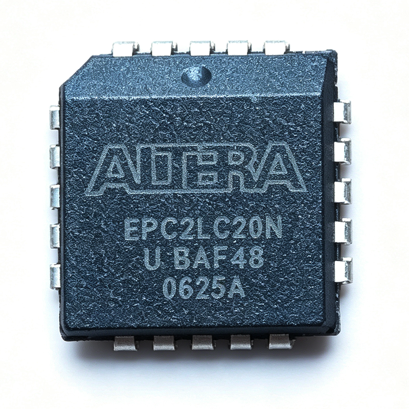
EPC2LC20 - 1.6Mb In-System Prog Config PROM 20-PLCC | Altera
The Altera EPC2LC20 is a 1.6-Mbit in-system programmable (ISP) configuration PROM designed to load configuration bitstreams into SRAM-based Altera FPGA families at power-up. Housed in a 20-pin J-lead PLCC (9x9 mm) package, the EPC2LC20 supports configuration data widths of x1 in serial mode and connects directly to Altera FPGAs such as ACEX 1K, APEX 20K/20KC/20KE, APEX II, Arria GX, Cyclone, Cyclone II, FLEX 10K, FLEX 6000, and MAX 9000 series. The device is rated for both 5.0-V and 3.3-V ISP through the built-in IEEE 1149.1 (JTAG) Test Access Port (TAP), enabling reconfiguration in-circuit without removing the device from the board. A configuration PROM is a non-volatile memory device that stores the FPGA's configuration bitstream and delivers it serially or in parallel to the target SRAM-based FPGA every time the system powers up or when new configuration data is needed. Because SRAM-based LUT devices are volatile, the EPC2LC20 eliminates the need for a separate boot ROM and reduces BOM cost, PCB area, and design complexity. The EPC2 family sits in the broader hierarchy of FPGA configuration memory: configuration PROM -> non-volatile boot memory -> FPGA companion IC -> programmable logic support silicon. Key features of the EPC2LC20 include 1.6 Mbits of storage capacity, cascadable JTAG-chain support so multiple EPC2 devices can be chained together to configure larger FPGAs, and dedicated open-drain CONF_DONE and nSTATUS pins for handshaking with the target FPGA. The device supports 8-bit or 16-bit JTAG boundary-scan, plus built-in data decompression compatible with Altera Quartus II programming files. Programming is performed via the Altera Programming Unit (APU) or any IEEE 1149.1-compliant JTAG controller. In terms of architecture, the EPC2LC20 is built around a CMOS non-volatile memory array with on-chip charge pumps for ISP operation. It exposes standard JTAG pins (TCK, TMS, TDI, TDO) plus dedicated nCONFIG, nSTATUS, CONF_DONE and DCLK interface pins to the FPGA, so no glue logic is required between the PROM and the FPGA. The JTAG-based ISP allows field upgrades and factory-floor programming using only a 4-wire JTAG cable. Typical applications include boot configuration for Cyclone and Cyclone II FPGA designs, APEX 20K family prototyping cards, multi-FPGA systems that daisy-chain several EPC2 devices in JTAG order, industrial controllers using FLEX 10K/6000 logic, and legacy designs that require a simple non-volatile companion to Altera SRAM-based FPGAs. When selecting between EPC2 variants, choose the EPC2LC20 for low-density designs and cascade additional EPC2s for larger FPGA bitstreams.
EPC2LC20-T - 1.6Mb FPGA Config PROM PLCC-20 | Altera
The Altera (Intel) EPC2LC20-T is a 1.6 Mb in-system programmable Configuration PROM for SRAM-based FPGAs, housed in a 20-pin PLCC package. It operates at up to 10 MHz serial configuration frequency and supplies non-volatile storage for Altera SRAM-LUT devices such as the ACEX, APEX, Cyclone, FLEX, MAX 7000A/B, MAX II, and Mercury families. The "-T" suffix indicates tape-and-reel packaging for high-volume surface-mount assembly. A Configuration PROM is a serial non-volatile memory that loads bitstream data into an SRAM-based FPGA at every power-up, because SRAM configuration cells are volatile. EPC2-series PROMs sit between the system's flash storage or microcontroller and the FPGA's DATA0/DCLK/nCONFIG/nSTATUS/CONF_DONE pins, presenting the bitstream serially via Altera's FPP or PS configuration schemes. This category sits inside the broader hierarchy: non-volatile memory -> PROM -> configuration memory -> FPGA boot device -> semiconductor. Key features of the EPC2LC20 include 1.6 Mb flash storage, in-system programmability through the JTAG IEEE Std 1149.1-1990 boundary-scan interface, and the ability to cascade multiple devices to support larger bitstreams. The device operates from a single 3.3 V supply and integrates a low-voltage detector that holds the FPGA in reset until VCC is stable, simplifying multi-rail power sequencing. The EPC2 uses a 4-pin serial interface (DATA, DCLK, nCONFIG, nSTATUS, CONF_DONE) compatible with Altera's PS configuration mode. Internally, a state machine manages configuration timing, CRC checking, and optional data compression. The JTAG port supports ISP (In-System Programming) so designers can update firmware in the field without removing the PROM. Typical applications include industrial control boards, military and aerospace FPGA systems, telecommunications line cards, medical imaging hardware, and test-and-measurement equipment using Altera/Intel FPGAs. The wide JTAG support also makes the EPC2LC20-T well suited for remote firmware updates. Design consideration: Because EPC2-series PROMs are pre-loaded via JTAG or the Altera Programming Unit, plan ISP access through the FPGA's JTAG chain or a dedicated header. When cascading multiple EPC2s, the nCASC pin propagates enable to the next device in the chain. This page consolidates distributor pricing, drop-in pin-compatible alternatives, and engineering design notes that extend beyond the original Altera datasheet.
EPC2LC20-U - 1.6Mb FPGA Config PROM, 20-PLCC | Altera (Intel)
The Altera EPC2LC20-U is an in-system programmable configuration PROM designed to load configuration bitstreams into Altera/Intel SRAM-based FPGAs at power-up, delivering 1.6 Mb of flash-backed configuration storage in a 20-pin PLCC (9x9) package with 10 MHz serial interface speed. It supports 3.3V operation and includes JTAG-based in-system programmability (ISP) via the IEEE 1149.1 boundary-scan chain, eliminating the need for an external programmer. A configuration PROM is a non-volatile memory device dedicated to storing the FPGA bitstream. On every power-up the FPGA's SRAM configuration cells must be reloaded because SRAM is volatile; the EPC2 family is purpose-built for this task and connects to the FPGA's dedicated serial configuration pins (DATA, DCLK, nCONFIG, nSTATUS, CONF_DONE). Compared with generic SPI flash, configuration PROMs reduce board complexity by offering a guaranteed-timing, drop-in storage device for legacy Altera APEX, FLEX, Cyclone, ACEX and Arria GX families. Key features include 1.6 Mb storage (sufficient for mid-density FPGAs), a 10 MHz serial configuration clock, in-system programmability via JTAG, cascadable architecture for larger bitstreams, and a low pin count 20-PLCC footprint that simplifies PCB layout. The device operates from 3.0V to 3.6V across the industrial -40C to +85C range. The EPC2 uses a 4-pin serial interface plus JTAG, with on-chip voltage generation for the program/erase charge pump and a built-in oscillator for internal timing. The cascadable feature allows two or more EPC2 devices to be chained to configure larger FPGAs, with the master/slave handoff handled automatically over the serial interface. Typical applications include legacy Altera APEX 20K / APEX II / ACEX 1K / FLEX 10K configuration, Cyclone and Cyclone II boot memory, Arria GX configuration, industrial control cards that pair a small FPGA with non-volatile storage, and any 3.3V system that needs reliable in-system reprogrammable configuration memory. The JTAG ISP capability also supports field firmware updates without removing the board. When designing with this part, place a 0.1 uF decoupling capacitor within 5 mm of VCC and keep the JTAG chain length under about 150 mm to preserve signal integrity. For bitstreams larger than 1.6 Mb, cascade a second EPC2 device - the FPGA's MSEL pins select the cascade mode and CONF_DONE handling is automatic. This page synthesizes distributor stock, verified drop-in alternatives such as EPC2LI20 and EPC2LC20N, lifecycle status, and design considerations not found in the bare datasheet.
EPC2LC20-V - 1.6Mb FPGA Config PROM, 20-PLCC | Altera
The Altera (Intel) EPC2LC20-V is a 1.6-Mbit in-system programmable Configuration PROM designed for configuring SRAM-based look-up table (LUT) FPGAs, housed in a 20-pin Plastic Leaded Chip Carrier (PLCC) package optimized for legacy through-hole and socketed production flows. A configuration PROM is a non-volatile memory device that stores the FPGA bitstream and loads it into the SRAM-based LUT device at power-up, reset, or upon reconfiguration request. Within the broader hierarchy, configuration PROMs sit at the boot-memory layer beneath FPGAs and CPLDs, between power-on reset events and the user logic — EPC1/EPC2 series parts specifically support Altera (now Intel) APEX 20K, ACEX 1K, FLEX 10K, FLEX 6000, and MAX 9000 device families, simplifying single-chip configuration and enabling remote in-system reconfiguration via JTAG. Key features include 1.6 Mbit of Flash-based configuration storage, a serial configuration interface clocked up to 10 MHz, in-system programmability through the IEEE 1149.1 (JTAG) boundary-scan port, and a cascadable daisy-chain interface that allows multiple EPC2 devices to be linked for designs exceeding the single-device capacity. The -V suffix indicates the commercial operating temperature range of 0 °C to +70 °C, while the LC family provides the low-cost tier of the EPC2 line. Technically, the EPC2LC20-V uses a 3.3 V core supply (VCC) with 5 V-tolerant I/O on configuration interface pins, four JTAG pins (TMS, TCK, TDI, TDO) supporting boundary-scan and ISP, and dedicated nCS, nSTATUS, CONF_DONE, and DCLK pins for the FPGA configuration handshake. The 20-pin PLCC package (JEDEC MS-018) provides a socket-friendly footprint suitable for prototyping sockets, field upgrades, and legacy replacement scenarios. Typical applications include configuring APEX 20K and ACEX 1K FPGA prototype boards, industrial control systems with field-upgradable logic, telecommunications line cards using FLEX 10K devices, and military/aerospace ground-test fixtures built around MAX 9000 parts. The 1.6 Mbit density is dimensioned for mid-density APEX 20K designs and most ACEX 1K configurations. Designers should budget for the dedicated JTAG header and ensure that the PROM-to-FPGA DCLK/nSTATUS/CONF_DONE handshake traces are kept short. For multi-PROM cascading, ensure that the cascaded chain does not exceed the FPGA's maximum configuration clock frequency or supported PROM count. This page consolidates distributor pricing, drop-in alternatives in the same 20-PLCC footprint, and practical design considerations not directly summarized in the Altera configuration-device datasheet — distinct information gain relative to manufacturer PDF and Octopart listings.
EPC2LC20CAD - 1.6Mb Config PROM for SRAM FPGAs | Altera
The Altera EPC2LC20CAD is a 1.6 Mb in-system programmable configuration PROM designed to load configuration data into SRAM-based Altera FPGAs such as the APEX, ACEX, Cyclone, and Stratix device families. It is housed in a 20-pin J-lead PLCC (PLCC-20) package and operates from a single 3.3V supply. The device supports serial (bit-wide) configuration of single FPGAs through a dedicated serial-data interface and can be cascaded for multi-device chains. An FPGA configuration PROM is a non-volatile memory device whose sole purpose is to store the bitstream image that an SRAM-based LUT FPGA needs at every power-up because SRAM cells lose their configuration when power is removed. The EPC2 family sits in the boot-memory hierarchy between the FPGA and the system host: at power-on the FPGA reads its bitstream serially from the PROM, then enters user mode. Modern Altera/Intel parts replaced the EPC2 family with active serial (AS) flash configuration devices, so the EPC2LC20CAD is now widely used as a drop-in legacy replacement and for repair/maintenance of installed systems. Key features include 1.6 Mb storage capacity, in-system programmability through the IEEE Std 1149.1 JTAG interface, 3.3V single-supply operation with 5V tolerant I/O, and a JTAG-based ISP that allows the bitstream to be updated on-board without removing the device. Programming is performed through the standard JTAG pins (TCK, TMS, TDI, TDO) so no dedicated programmer socket is required, simplifying manufacturing flow. The EPC2 architecture is a serial Flash PROM optimized for one-time-or-occasional update use rather than high-endurance writes. Internally it contains an oscillator, address counter, and serial interface state machine that streams the configuration bits to the FPGA. The 20-pin PLCC package provides a through-hole or socketed footprint that was standard for late-1990s and early-2000s Altera reference designs. Typical applications include Altera APEX 20K, ACEX 1K, Cyclone (original), and Stratix FPGA configuration in industrial controllers, telecommunications line cards, and legacy networking equipment. The device is also used in test fixtures and as a repair/maintenance part for legacy Altera boards where the original configuration PROM has failed or needs to be re-programmed. When designing with this device, ensure the JTAG chain is properly terminated and that the PROM's nSTATUS/CONF_DONE handshaking matches the target FPGA's configuration mode. The 3.3V supply must be stable before the FPGA releases its nCONFIG signal, otherwise the FPGA may enter an undefined state and require re-configuration. This page synthesizes distributor pricing, drop-in alternatives, and practical design notes not found on the manufacturer datasheet alone, providing engineers with a single reference for sourcing and replacement decisions.
EPC2LC20ES - 1.6Mb ISP Config PROM for FPGAs | Intel / Altera
The Intel (formerly Altera) EPC2LC20ES is an in-system programmable (ISP) configuration memory device designed for SRAM-based FPGAs and LUT devices, providing 1.6 Mbit of non-volatile storage in a 20-pin PLCC (J-lead) package. The device stores configuration bitstreams that are loaded into the FPGA's SRAM configuration cells at power-up, and supports 5.0 V and 3.3 V operation including in-system programmability through the built-in IEEE Std. 1149.1 JTAG interface. The EPC2LC20ES is functionally equivalent to the EPC2LC20 with the "ES" suffix denoting a specific lead-free or industrial temperature grade variant. A Configuration PROM (Programmable Read-Only Memory) for FPGAs is a non-volatile serial memory device that holds the FPGA's configuration bitstream. When the FPGA powers up, it reads its configuration data from the PROM via a serial or parallel configuration interface. These devices sit in the broader memory hierarchy as: PROM -> non-volatile memory -> configuration memory -> FPGA support IC, and are essential for standalone FPGA designs that need to self-configure without an external microprocessor or download cable. Key features of the EPC2LC20ES include 1.6 Mbit storage capacity suitable for mid-density Altera FPGAs such as the ACEX 1K, APEX 20K, Cyclone, and Mercury families, JTAG-based ISP that allows field upgrades without removing the device, and built-in JTAG boundary-scan test (BST) circuitry compliant with IEEE Std. 1149.1. The device supports both DCLK-based serial and parallel configuration modes, providing flexibility across multiple FPGA targets. Low standby current and 3.3 V/5 V tolerance make it well suited for mixed-voltage system designs. Architecturally, the EPC2LC20ES uses a serial interface with a built-in oscillator and state machine that streams configuration data to the FPGA through the DATA, DCLK, and nCONFIG/nSTATUS control signals. The on-chip JTAG TAP controller enables both ISP and boundary-scan test access. The PROM operates as a slave device on the JTAG chain, allowing multiple devices to be programmed and verified in a single boundary-scan pass. Typical applications include configuration storage for Altera ACEX 1K, APEX 20K, Cyclone, Mercury, and Stratix-class FPGAs, factory-floor JTAG programming stations, and field-upgradable embedded systems. Designers also use this PROM in industrial controllers and military/aerospace prototypes where a self-booting FPGA is required without an external configuration controller. When designing with this device, note that the EPC2LC20ES is rated for industrial temperature range and ships as a lead-free PLCC-20 J-leaded package for through-hole or socketed mounting. The device is in production but considered a legacy Altera configuration solution; for new designs, designers should evaluate Altera/Intel EPCQ-series serial configuration devices (AS mode) for newer FPGA families. This page synthesizes distributor pricing, same-brand and cross-brand drop-in alternatives, and practical design notes not found in the manufacturer datasheet, helping engineers quickly validate EPC2LC20ES as a configuration memory solution for legacy and current Altera FPGA designs.
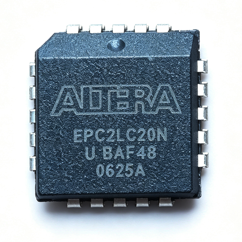
EPC2LC20N - 1.6Mb FPGA Configuration PROM, 20-PLCC | Intel
The Intel (formerly Altera) EPC2LC20N is a 1.6-Mbit in-system programmable Flash configuration PROM designed to load configuration bitstreams into SRAM-based LUT FPGAs at every power-up. Housed in a 20-pin PLCC (J-lead, 9x9 mm) package, it operates from dual-rail supplies of 3.0 V to 3.6 V and 4.75 V to 5.25 V, supports JTAG-ISP (IEEE 1532 / IEEE 1149.1) and Altera serial configuration modes, and runs the configuration clock up to 8 MHz. A configuration PROM (Programmable Read-Only Memory) is a non-volatile serial memory device whose sole purpose is to store the bitstream for an SRAM-based programmable logic device. Because SRAM-LUT FPGAs are volatile, their configuration must be reloaded on every power-up or reconfiguration event; the EPC2 family performs that role in a single-chip solution, replacing discrete EPROMs, microcontrollers, or boot-PROM arrangements. EPC2 devices sit in the boot-source hierarchy beneath FPGAs (CPLD -> glue logic -> PROM -> FPGA) and are an integral part of the Altera/Intel FPGA power-on sequencing ecosystem. Key features of the EPC2LC20N include 1.6 Mbit of Flash storage, in-system programmability via JTAG, a built-in 8 MHz internal oscillator, and support for both 3.3 V and 5 V supply rails. It also provides a dedicated nSTATUS, nCONFIG, and CONF_DONE handshake to the target FPGA, eliminating the need for external glue logic in most designs. The EPC2LC20N uses a 4-pin serial interface (DATA0, DCLK, nCONFIG, nSTATUS) to cascade-multiple PROMs can be chained to support larger FPGAs. The device supports FPGAs from the Altera APEX, Cyclone, Stratix, ACEX, and MAX 7000 families, with automatic baud-rate detection between the PROM and target device. Typical applications include Altera/Intel Cyclone and APEX prototype boards, industrial control logic, telecom base-station FPGA boot cards, military/aerospace FPGA subsystems, and any system requiring multi-configuration support. The in-system programmability allows field upgrades without removing the PROM from the board. When designing with this device, ensure proper decoupling (0.1 uF + 10 uF) on both VCC rails and respect the JTAG chain order if multiple PROMs are cascaded. The 5 V rail tolerance simplifies designs that mix 3.3 V FPGA I/O with 5 V configuration memory logic. This page synthesizes distributor stock levels, drop-in Altera/Intel PROM alternatives, and JTAG-chain design notes not found on the original manufacturer datasheet.
EPC2LC20N-W - 1.6Mb In-System Prog Config PROM | Altera | PLCC-20
The Intel/Altera EPC2LC20N-W is a 1.6-Mbit in-system programmable (ISP) configuration PROM designed for serial configuration of SRAM-based LUT FPGAs such as APEX 20K, ACEX 1K, Mercury, FLEX 10K, Stratix, and Cyclone families. It is supplied in a 20-pin PLCC (J-lead) package with a 3.0V-3.6V or 4.75V-5.25V dual-rail supply range and supports 66.7 MHz internal oscillator-based serial data delivery. The "-W" suffix denotes the tape-and-reel packaging option of the base EPC2LC20N part. A configuration PROM is a non-volatile memory that stores FPGA bitstream data and serially transfers it to the target FPGA at power-up via the DATA, DCLK, OE, and nCS handshake lines. In the broader hierarchy, the EPC2 sits under Altera's enhanced-configuration-device family (EPC4/EPC8/EPC16/EPC2/EPC1/EPC1441), which itself belongs to the FPGA-support ecosystem (configuration memory -> memory IC -> semiconductor). The 3.3V/5V dual supply, JTAG ISP support, and 1.6-Mbit density make the EPC2LC20N-W one of the most widely used legacy Altera configuration devices. Key features include 1.6 Mbit EPROM density, serial configuration clock up to 66.7 MHz, in-system programmability through the JTAG (Joint Test Action Group) interface, 4-pin serial interface (DATA, DCLK, nCS, OE), and support for cascading with other EPC devices. The device is non-cascadable in the enhanced-configuration-device family when targeting newer high-density Stratix FPGAs; for those applications Altera recommends EPC4/EPC8/EPC16. The EPC2LC20N-W uses an EPROM core that is erased by UV exposure (windowed package variants) and reloaded via JTAG. The internal address counter is clocked by DCLK from the target FPGA, while nCS and OE gate the tri-state DATA output. The combination of a small footprint and a robust serial protocol has made the EPC2 a de-facto standard for APEX 20K and ACEX 1K designs. Typical applications include APEX 20K / ACEX 1K / FLEX 10K FPGA boot configuration, Stratix-series configuration on legacy boards, industrial control system FPGA boot memory, and test equipment FPGA bitstream storage. For designs migrating to Cyclone III/IV/V or Stratix V/10, Altera recommends newer configuration devices or active serial flash. Designers should verify that the target FPGA is compatible with the EPC2 device family using the Altera Configuration Device Compatibility table before PCB layout. The 20-pin PLCC J-lead package requires a socket or reflow profile compatible with J-leaded devices. This page synthesizes distributor pricing, drop-in alternatives, pinout data, and practical design notes not found in the manufacturer datasheet. Lifecycle, supply voltage, and pinout values are extracted verbatim from the Altera EPC2 Configuration Devices datasheet.
EPC2LC20NA - 1.6Mb ISP Config PROM | Altera | PLCC-20
The Altera EPC2LC20NA is an in-system programmable (ISP) Configuration PROM designed to configure SRAM-based LUT FPGAs such as Altera APEX, ACEX, FLEX, and Cyclone families, providing 1.6 Mb of configuration memory in a 20-pin PLCC package. It supports 3.3V operation and is offered in industrial operating temperature grade. A configuration PROM (Programmable Read-Only Memory) is a non-volatile memory device that stores FPGA bitstream data and delivers it to the FPGA at power-up via a serial configuration interface. The EPC2 family belongs to the broader category of FPGA configuration memory, sitting hierarchically under programmable logic boot/storage and above generic serial PROMs. Engineers select configuration PROMs based on bitstream size, target FPGA density, voltage compatibility, and in-system reprogrammability. Key features of the EPC2LC20NA include 1.6 Mbit density, in-system programmability via IEEE 1532 JTAG, 3.3V VCC operation, and a serial configuration data output to the target FPGA. The device supports multi-device daisy-chaining and offers short programming/erase times compared to legacy EPC1 alternatives. The PLCC-20 (9x9 mm) through-hole-compatible surface-mount package facilitates socketed programming and field-replacement workflows. The EPC2LC20NA utilizes Altera's proven floating-gate memory cell array with on-chip charge pumps and a serial state machine that handles the configuration handshake with the host FPGA. The JTAG interface complies with IEEE Std 1149.1 boundary-scan and IEEE 1532 ISP, allowing bitstream updates without removing the device from the PCB. The internal oscillator and timing logic drive the configuration clock to the FPGA in passive serial (PS) mode, eliminating the need for an external configuration clock source. Typical applications include boot configuration for Altera APEX 20K, ACEX 1K, FLEX 10K, FLEX 6000, Cyclone, and Mercury FPGA devices; industrial control boards; telecom line cards; and prototyping platforms requiring field firmware updates. The 1.6 Mb capacity comfortably fits bitstreams for mid-density FPGAs up to approximately 200,000 gates. When designing with EPC2LC20NA, ensure the configuration mode (passive serial) of the target FPGA is selected and that the MSEL pins are set accordingly. Place a decoupling capacitor close to VCC and observe JTAG chain ordering when multiple devices share the same TAP controller. This page synthesizes distributor stock levels, drop-in same-package alternatives, and design considerations not found in the manufacturer datasheet, providing practical guidance for legacy system maintenance and new designs targeting Altera FPGA families.
EPC2LC20NU - 1.6Mb ISP Config PROM 20-PLCC | Intel / Altera
The Intel / Altera EPC2LC20NU is a 1.6-Mbit in-system programmable (ISP) configuration PROM designed to store and deliver configuration bitstreams to SRAM-based LUT FPGAs in the Altera / Intel device family, housed in a 20-pin J-lead PLCC package suitable for surface-mount production lines. An FPGA configuration PROM is a non-volatile memory device that holds the bitstream used to program a volatile SRAM-based FPGA at every power-up. Because SRAM LUTs lose their configuration when power is removed, every system containing an SRAM FPGA requires an external boot memory - either a configuration PROM, a flash, or a microcontroller that emulates the configuration bus. EPC2-series devices implement Altera's serial configuration protocol (compatible with FPGAs such as APEX, Cyclone, and older families) and are re-programmable in-system via JTAG, removing the need for a stand-alone programmer in production. Key features of the EPC2LC20NU include 1.6 Mb of usable configuration memory, an industry-standard 4-pin serial configuration interface (nCS, DCLK, DATA, nINIT_CONF), in-system programmability through the IEEE 1149.1 JTAG port, 3.3 V core supply with 5 V tolerant I/O on most pins, and built-in cascading support so multiple EPC2 devices can be daisy-chained to configure FPGAs larger than 1.6 Mb. The J-lead PLCC-20 footprint has been a long-standing Altera configuration standard and matches the land pattern of earlier EPC1 devices. Technically the EPC2LC20NU is built on a floating-gate CMOS process with on-chip charge pumps to support in-system erase and reprogram cycles without external high voltages. The 4-pin interface lets the host FPGA generate DCLK and read DATA, while a dedicated nINIT_CONF / OE pin releases the bus at power-up or after a reconfiguration event. Programming endurance is rated in the thousands of cycles with data retention measured in decades, allowing field firmware updates. Typical applications include Altera APEX II, APEX 20K, Mercury, FLEX 10K, ACEX 1K, and Cyclone-series SRAM-based LUT FPGAs in industrial controllers, telecom line cards, and military / aerospace prototypes that still rely on the legacy serial configuration protocol. Designers should pair the EPC2LC20NU with the appropriate Altera Quartus configuration file format and verify that the target FPGA bitstream size does not exceed the 1.6 Mb capacity.
EPC2LC21N - Altera/Intel Configuration PROM for SRAM FPGAs
The Altera/Intel EPC2LC21N is a 1.6-Mbit in-system-programmable configuration PROM designed to load configuration bitstreams into Altera SRAM-based FPGAs and Complex Programmable Logic Devices (CPLDs). It is supplied in a 20-pin PLCC package and supports 3.3V operation, making it a drop-in companion for legacy Altera APEX, ACEX, FLEX, Cyclone, and MAX-series FPGAs. The device uses a simple serial configuration interface and provides JTAG-based in-system programmability (ISP), which allows the configuration bitstream to be updated on the populated PCB without removing the part. A configuration PROM is a non-volatile memory device that stores the FPGA's configuration bitstream and presents it serially to the target FPGA at power-up. It belongs to the broader category of non-volatile memories, sitting hierarchically between EPROM/EEPROM and flash, and serves as a one-chip boot source for SRAM-based programmable logic. The EPC2 family combines the configuration storage role with ISP, so designers can rework a board's logic image without hot-air rework or socket swaps. Key features of the EPC2LC21N include 1.6 Mbit of configuration storage, 3.3V single-supply operation, JTAG-ISP support, an open-drain CONF_DONE signal for handshaking with the FPGA, and a low-power CMOS process. The serial interface minimizes FPGA pin consumption, while the JTAG path supports boundary-scan and field upgrades. The PLCC-20 footprint is through-hole friendly and remains compatible with older Altera reference designs that predate the migration to surface-mount EPCQ/QSPI flash. The EPC2LC21N's underlying technology is a high-density EPROM/EEPROM-style cell array with on-chip charge-pump programming logic, wrapped in a controller that streams data to the FPGA's DCLK/DATA pins. The part is designed for unlimited configuration reads (FPGA always reads at POR) and a finite ISP-write endurance. Its 3.3V I/O and lack of a separate program voltage supply simplify power-tree design relative to older 5V EPC1 parts. Typical applications include legacy Altera APEX 20K and FLEX 10K configuration loading, industrial control boards that still ship on Altera MAX/Cyclone FPGAs, prototyping carriers, and field-upgradeable logic modules. The PLCC package is particularly attractive for through-hole assembly and for repair-friendly board designs in industrial equipment. When designing with this part, route the JTAG chain (TCK/TMS/TDO/TDI) so the EPC2 shares the FPGA's boundary-scan path; this enables in-system reconfiguration via a single Altera USB-Blaster or ByteBlaster. Confirm that the target FPGA's configuration mode selects serial PROM and that the EPC2's nCS pin is wired to the correct FPGA nSTATUS or mode pin. Leave nINIT_CONF tied correctly per the Altera configuration handbook to avoid false reconfiguration cycles. This page synthesizes distributor pricing, drop-in alternatives, and practical design notes not found in the manufacturer datasheet, giving engineers a single source for lifecycle, replacement, and application guidance on the EPC2LC21N.
EPC2LC22N - 1.6Mb Altera Configuration PROM | PLCC-22
The Altera EPC2LC22N is an in-system programmable configuration PROM designed for loading configuration bitstreams into SRAM-based Altera FPGAs. According to the EPC2 configuration device datasheet from Intel/Altera, the part stores 1.6 Mbits of configuration data and is offered in a 22-pin Plastic Leaded Chip Carrier (PLCC-22) package with through-hole mounting. A configuration PROM is a non-volatile memory device that holds the FPGA's configuration bitstream. When the FPGA powers up, it reads its configuration data from a configuration PROM (typically via JTAG or a dedicated serial interface). Configuration PROMs belong to the broader category of non-volatile memory ICs and serve as boot memory for SRAM-based FPGAs (which lose their configuration when power is removed). The EPC2 family specifically targets Altera's legacy APEX, Mercury, ACEX, Cyclone, and Stratix FPGAs. Key features of the EPC2LC22N include in-system programmability via IEEE 1149.1 (JTAG) boundary-scan, cascadable architecture for multi-device configuration chains, and low-power CMOS technology. The device supports Altera's serial configuration protocol and can be cascaded to support arbitrarily large bitstreams. The 2.5V core (LC designation) provides lower power consumption than the 5V and 3.3V variants in the EPC2 family. The EPC2LC22N uses a 4-pin JTAG interface (TCK, TMS, TDI, TDO) for in-system programming, eliminating the need for a separate PROM programmer. The cascadable design allows multiple EPC2 devices to be chained together to configure FPGAs with bitstreams larger than 1.6 Mbits. The device includes an internal oscillator and timing control, simplifying board design by removing the need for external configuration clock generation. Typical applications include legacy Altera APEX 20K / APEX II FPGA configuration, ACEX 1K boot memory, Mercury device support, and embedded systems requiring in-field FPGA reconfiguration via JTAG. The PLCC-22 through-hole package is suited for prototyping, legacy board designs, and applications where socketed configuration memory is preferred for field serviceability. When designing with the EPC2LC22N, ensure the JTAG chain is properly terminated and the FPGA's MSEL pins are set to the correct configuration mode for serial PROM boot. Note that this part is now in legacy status and is replaced in many new designs by newer Cyclone/MAX series FPGAs with built-in flash configuration memory, eliminating the external PROM altogether. This page synthesizes Intel/Altera datasheet information, distributor pricing, and drop-in compatible EPC2 family alternatives not found in a single manufacturer document, providing practical sourcing guidance for legacy FPGA design maintenance.
EPC2LC2QN - 2Mb SRAM-Based LUT FPGA Config Device | Altera
The Altera EPC2LC2QN is a 2-megabit serial configuration device designed to load configuration data into SRAM-based Altera FPGAs that use LUT (look-up table) architecture, including the APEX II, Cyclone, and Stratix device families. The device supports a 3.3V core supply, operates from 0°C to +70°C commercial temperature range, and is housed in a 100-pin PQFP package. According to Altera (now Intel FPGA) configuration-device collateral, the EPC2LC2QN supports flexible configuration schemes including JTAG-based in-system programmability and serial daisy-chain multi-device configuration, enabling designers to update bitstreams in the field without removing the FPGA from the board. A configuration device is a non-volatile serial Flash memory specifically engineered to store and stream FPGA configuration bitstreams to an SRAM-based LUT FPGA at power-up. Because SRAM-based LUT devices lose their configuration when power is removed (volatile technology), a companion configuration device such as the EPC2LC2QN is required to reload the bitstream on every POR (power-on reset) event. This category sits within the broader hierarchy of non-volatile memory ICs, parallel and serial boot Flash devices, and FPGA configuration memory, and is essential to any system that uses SRAM-based LUT FPGAs. Key features include 2 Mb of configuration storage, a 4-wire serial interface to the host FPGA (DATA, DCLK, nCONFIG, nSTATUS), in-system programmability through the JTAG (IEEE 1149.1) boundary-scan interface, support for multi-device daisy-chain configuration of up to 8 FPGAs, and built-in decompression of Altera-compressed bitstreams. The 100-pin PQFP (Plastic Quad Flat Pack) surface-mount package provides sufficient pin count for the configuration control signals and JTAG test access port, while maintaining a compact board footprint compared to older PLCC packages. Technically, the EPC2LC2QN uses an internal oscillator to generate the configuration clock (DCLK) and supports both serial and parallel configuration modes. The device accepts compressed bitstreams from the Quartus II / Quartus Prime programmer and decompresses them on the fly before forwarding to the target FPGA, effectively doubling the usable storage. The 3.3V single-supply operation simplifies power-tree design in 3.3V-centric boards that pair with APEX II or first-generation Cyclone FPGAs. Typical applications include Altera APEX II EP2A15/EP2A25/EP2A40 configuration, Cyclone EP1C3/EP1C4/EP1C6/EP1C12 boot, Stratix EP1S10/EP1S20/EP1S25 memory loading, JTAG-based field firmware update in industrial controllers, and multi-FPGA prototyping boards where daisy-chain configuration reduces board complexity. Designers also use the EPC2LC2QN in legacy migration designs that must remain pin-compatible with older Altera reference schematics. When designing with this device, ensure the JTAG chain includes the configuration device's TMS, TCK, TDI, and TDO pins wired in series with the FPGA's JTAG port to allow boundary-scan programming. Verify the VCC ramp time meets the 100 µs minimum required by the EPC2 configuration controller to avoid POR ambiguity. This page synthesizes distributor pricing, drop-in Altera-family configuration alternatives, and practical design notes not collected in the standalone Altera datasheet.
EPC2LI20 - 1.6Mb In-System Prog Config PROM | Altera | PLCC-20
The Altera EPC2LI20 is a 1.6-Mbit in-system programmable configuration PROM designed for SRAM-based Altera FPGAs, housed in a 20-pin J-leaded Plastic Leaded Chip Carrier (PLCC-20, 9x9 mm) package and specified for the industrial -40C to +85C operating range. It supports 3.3V (3.0-3.6V) and 5.0V (4.5-5.5V) supply operation, offers 1.6 megabits of flash storage, and integrates Altera's enhanced configuration controller with on-chip decompression that allows compressed configuration bitstreams to be stored in less memory space than the corresponding FPGA design requires. What is a configuration PROM? A configuration PROM (Programmable Read-Only Memory) is a non-volatile memory device that holds the FPGA's configuration bitstream and reloads it into the SRAM-based LUT fabric every time the system powers up, initializes, or needs new configuration data. Because SRAM FPGAs lose their logic configuration when power is removed, they require an external boot memory source; configuration PROMs sit at the bottom of the programmable-logic memory hierarchy (PROM -> volatile configuration memory -> FPGA logic fabric) and remain the simplest drop-in boot-source solution for legacy Altera/Intel FPGA designs. The EPC2 device family combines a flash memory array with an internal controller that handles the serial or parallel configuration interface to one or more Altera FPGAs. Key features include in-system programmability via IEEE 1532 JTAG, on-chip voltage-sensing circuitry that automatically selects 3.3V or 5.0V operation, support for both serial and parallel (byte-wide) configuration modes, and a programmable decompression engine that lets compressed bitstreams occupy as little as 35% of the equivalent uncompressed image. The flash also offers user-accessible memory space that can be used by a Nios embedded processor or external PLD for general-purpose non-volatile storage. In typical designs the EPC2LI20 connects directly to the FPGA's DATA, DCLK, nCONFIG, nSTATUS, and CONF_DONE pins, with JTAG signals (TCK, TMS, TDI, TDO) brought out for in-system programming. The controller sequences the configuration automatically after POR, monitors nSTATUS, and can chain-load additional FPGAs in a multi-device configuration chain. Because configuration is read out of flash serially or by byte, the EPC2LI20 supports both legacy FPGAs and Altera's MAX II, Cyclone, Stratix, and APEX device families. Common applications include industrial control boards, factory automation equipment, telecom line cards, and legacy FPGA-based test platforms that need a compact through-hole boot memory. Choose EPC2LI20 when the design uses a PLCC-20 footprint and must operate from -40C to +85C; choose EPCQ or EPCQ-A configuration devices for new designs where Intel/Altera recommends migrating from EPC2-series PROMs. When designing with the EPC2LI20, route JTAG signals as a star from a single header so that the chain can be re-programmed in-system without disturbing other board-level signals. Place a 0.1 uF decoupling capacitor as close as practical to the VCC and VPP pins, and verify that nCONFIG and nSTATUS are pulled to the correct logic level through 10 kohm resistors. The PLCC-20 footprint accommodates both socketed and direct-solder mounting; sockets are preferred for production programming. This page synthesizes distributor pricing, drop-in alternatives sourced from the Altera/Intel cross-reference data, and practical design notes that complement the manufacturer datasheet.
EPC2LI20J - 1.6Mb ISP Config PROM 20-PLCC | Altera
The Altera EPC2LI20J is an in-system programmable (ISP) configuration PROM with 1,695,680 bits (1.6Mb) of flash memory, designed to configure SRAM-based Altera FPGAs including APEX II, APEX 20K (20K, 20KC, 20KE), Mercury, ACEX 1K, and FLEX (6000, 10KE, 10KA) device families. Housed in a 20-pin PLCC package with J-leads, the device operates from a 3.3V supply (5V-tolerant I/O) and provides a simple 4-pin serial interface to the host FPGA, making it a drop-in replacement companion to legacy configuration schemes. The "J" suffix denotes the J-lead PLCC-20 package variant of the EPC2 family, distinct from the EPC2LI20 (standard PLCC-20) and EPC2TC32 (32-pin TQFP). An FPGA configuration PROM is a non-volatile serial flash device that stores the FPGA's bitstream and presents it to the FPGA at power-up via a serial configuration protocol, replacing parallel EEPROMs and reducing board area and pin count. The EPC2 family sits in the broader taxonomy: configuration PROM -> non-volatile memory -> serial flash -> semiconductor memory. It is a companion device rather than a general-purpose memory and is only ever used as part of an Altera FPGA boot circuit. Key features of the EPC2LI20J include 1.6Mb flash storage with 8-bit data width internally serialized through the Altera serial configuration interface, ISP programmability via JTAG, multi-device cascade support for configuring multiple FPGAs from a single chain, and a built-in oscillator that eliminates the need for an external configuration clock. The device is supported by the legacy Altera Quartus II programmer (PS mode) and remains in production for long-life industrial and military programs that maintain APEX/FLEX/Mercury designs. Typical applications include APEX II, APEX 20K, ACEX 1K, FLEX 6000, FLEX 10KE and Mercury FPGA configuration memory, factory-floor industrial controllers using FLEX 10KA, and military/aerospace programs with long-life FPGA designs. The PLCC-20 through-hole/socketed form factor suits designs where field reprogrammability or in-system recovery is required. When designing with the EPC2LI20J, follow Altera's reference schematic: route MSEL pins on the target FPGA to FPP/PS mode, connect nCONFIG/nSTATUS between PROM and FPGA, and ensure the JTAG chain order matches the Quartus programmer file. A 0.1uF decoupling capacitor close to VCC is mandatory. This page consolidates distributor stock, same-brand drop-in alternatives, and configuration-design notes not found in the standalone Altera datasheet.
EPC2LI20N - 1.6Mb FPGA Config PROM, 20-PLCC | Altera
The Altera EPC2LI20N is an in-system programmable configuration PROM with 1.6 Mbit of Flash memory designed to load configuration bitstreams into SRAM-based Altera FPGAs such as APEX II, Cyclone, Stratix II, and ACEX 1K series. Housed in a 20-pin PLCC (J-Lead) package measuring 9x9 mm, the part supports serial configuration at up to 10 MHz and operates from a dual voltage range of 3.0V to 3.6V and 4.5V to 5.5V. A configuration PROM is a non-volatile memory device that stores the FPGA bitstream and serially shifts it into the FPGA during power-up or reconfiguration. The EPC2 belongs to the broader family of programmable read-only memory (PROM) -> serial configuration memory -> FPGA configuration devices -> memory ICs taxonomy. It uses a JTAG-driven in-system programmability model so designers can re-flash the configuration image on populated boards without removing the device, which dramatically simplifies field upgrades and debugging. Key features include 1.6 Mbit Flash memory density, 20-pin PLCC (J-Lead) packaging, JTAG-based ISP, 3.0V/5.0V dual supply support, and a serial configuration clock rate up to 10 MHz. The device exposes standard Altera serial configuration signals (nCS, DCLK, DATA, nCONFIG, nSTATUS, CONF_DONE) so it interfaces to legacy Altera FPGA configuration controllers without glue logic. The EPC2LI20N uses a 4-pin serial interface to stream configuration data, with the FPGA acting as the configuration master. Internal oscillator and JTAG controller remove the need for external programming hardware, while in-system programming is supported via IEEE 1149.1 boundary scan. The result is a small-footprint, low-pin-count configuration solution that fits alongside the FPGA on the same PCB. Typical applications include configuring Altera Cyclone series FPGAs in industrial controllers, Stratix II FPGAs in telecommunications line cards, and APEX II devices in DSP co-processing boards. It is also used in test and measurement equipment that requires field-updatable configuration. When designing with this device, ensure the JTAG chain order is correct when multiple JTAG devices share the same TCK/TDI/TMS bus. The dual-supply design requires both 3.3V and 5V rails (or a single 3.3V rail with appropriate level shifting) to be present during configuration. This page synthesizes distributor pricing, drop-in PLCC-20 alternatives from the Altera/Intel EPC family, and PCB-layout design notes not found in the manufacturer datasheet alone.
EPC2LI20PULLS - 1.6Mb FPGA Configuration PROM, 20-PLCC | Intel
The Intel (formerly Altera) EPC2LI20PULLS is a 1.6-megabit in-system programmable configuration PROM designed to load configuration data into SRAM-based FPGAs such as the APEX, ACEX, Cyclone, and Stratix device families. Housed in a 20-pin PLCC (J-Lead) package, this serial-configuration memory stores up to 1.6 Mbits of compressed configuration data that is decompressed inside the FPGA during the configuration sequence. The "PULLS" suffix on the MPN denotes the specific factory tape-and-reel packaging and the orderable part variant shipped by Altera/Intel for surface-mount production lines. A configuration PROM is a non-volatile serial-flash memory whose sole purpose is to load bitstream data into an SRAM-based FPGA every time the system powers up or whenever a reconfiguration is required. Because SRAM FPGAs lose their configuration on power-down, a boot memory is required. EPC-series PROMs are part of the Altera enhanced configuration family that supports multi-device cascade chains, real-time decompression (which effectively multiplies storage density by 2x in typical workloads), and 8-/16-bit data-width modes for higher throughput on larger FPGAs. Key technical features of the EPC2LI20 include a 10 MHz maximum configuration clock rate, a 3.3 V core supply with 5 V tolerant I/O on configuration pins, in-system programmability through an IEEE 1149.1 JTAG interface, and built-in error-checking circuitry that aborts configuration if any bitstream error is detected. The device supports daisy-chained programming of multiple PROMs so a single JTAG link can program a chain of configuration devices on the board. Unused flash regions are also accessible by a Nios processor or other PLD for general-purpose non-volatile storage. Typical applications include FPGA configuration bitstream storage for Altera/Intel Cyclone, Stratix, APEX, ACEX, Mercury, and Excalibur FPGA families, JTAG-programmable production line bitstream loading, multi-board systems where configuration data must cascade between FPGAs, and embedded designs that reuse spare flash space for firmware or user data. The PLCC-20 footprint is the JEDEC-standard 20-lead plastic-leaded chip-carrier, suitable for socketed or surface-mount assembly and compatible with legacy Altera reference designs. When designing with EPC2LI20PULLS, ensure that the JTAG chain order matches the schematic, leave nCONFIG/nSTATUS lines properly pulled, and verify that the configuration bitstream is generated for the EPC2's compression mode. Engineers targeting newer Intel Cyclone 10 or Stratix 10 devices should instead use the EPCQ-series or the on-chip configuration subsystem of modern FPGAs, since the EPC2 is intended for legacy SRAM-based LUT families.
EPC2LI20U - 1.6Mb In-System Prog Config PROM | Altera | FPGA
The Altera EPC2LI20U is a 1.6-megabit in-system programmable configuration PROM designed to configure SRAM-based Altera FPGA devices, supplied in a 20-pin PLCC (9x9) package. The 'U' suffix indicates an industrial temperature grade rated for -40C to +85C operation, while the 'L' denotes a 3.3V or 5.0V tolerant supply and the 'I' designates an in-system programmable architecture with 4-pin serial interface. A configuration PROM is a non-volatile serial memory device that stores the FPGA's bitstream and loads it into the SRAM-based logic fabric at power-up. Because Altera SRAM-based LUT devices (APEX II, APEX 20K family, Mercury, ACEX 1K, and FLEX 6000/10KE/10KA) lose configuration when power is removed, an external configuration memory such as the EPC2LI20U is required to reload the device on every power-up cycle. The EPC2 family uses a simple 4-pin serial interface (DATA, DCLK, nCS, and OE) for easy connection to the FPGA's configuration pins. Key features include 1.6Mb storage density (sufficient for mid-density FPGAs), in-system programmability via IEEE 1149.1 JTAG, cascading capability to support larger bitstreams via dedicated nCASC pin, and 5.0V tolerant I/O on a 3.3V core supply. The device supports a serial configuration clock (DCLK) up to 33 MHz in fast mode and 17 MHz in standard mode, enabling rapid FPGA initialization. The PLCC-20 package provides through-hole compatibility for legacy designs and industrial systems. The EPC2 architecture uses a serial EEPROM-based storage array with on-chip charge pump for programming voltage generation. The in-system programmability eliminates the need for separate PROM programmers, reducing manufacturing cost and enabling field firmware updates through the JTAG chain. Each device is identified by a unique 32-bit device ID readable through JTAG for board-level traceability. Typical applications include configuring Altera APEX 20K, ACEX 1K, Mercury, and FLEX 6000/10KE/10KA FPGAs in telecommunications equipment, industrial control systems, test and measurement instrumentation, and legacy military/aerospace systems. The wide 3.3V-5.0V supply range allows the PROM to share the FPGA's programming voltage rail, simplifying board design. When designing with the EPC2LI20U, ensure that the nCS, DCLK, DATA, and OE traces are routed as short as possible to minimize skew and maintain signal integrity at the maximum DCLK frequency. For bitstreams exceeding 1.6Mb, cascade a second EPC2 device using the nCASC pin. Verify JTAG chain ordering to avoid configuration failures when multiple devices share the same programming bus. This page synthesizes distributor stock data, same-brand drop-in alternatives, and practical board-level design notes not aggregated in the Altera configuration handbook.
EPC2LS20U - 1.6Mb FPGA Config PROM, 20-PLCC | Altera
The Altera EPC2LS20U is a 1.6-megabit in-system programmable configuration PROM designed to configure SRAM-based LUT FPGAs such as the Altera Cyclone, Stratix, APEX, ACEX, and FLEX series. Packaged in a 20-pin PLCC (J-lead) outline, this device operates from a 3.3V supply and supports ISP (in-system programmability) through either a JTAG interface or the Altera proprietary programming mode, eliminating the need for a separate programmer. The "L" in the part number denotes the 3.3V core variant of the EPC2 family, the "S" indicates the specific density/pinout, and "20U" identifies the 20-pin PLCC package with Pb-free/RoHS-compliant lead finish. What is a configuration PROM? A configuration PROM is a non-volatile serial memory that stores the FPGA's bitstream and serially loads it into the SRAM-based configuration cells of an FPGA on power-up. Because SRAM FPGAs lose their configuration when power is removed, a configuration PROM is required to bootstrap the device at every power cycle. The PROM-to-FPGA chain forms part of the broader hierarchical taxonomy: non-volatile memory -> PROM/EPROM/EEPROM/Flash -> serial configuration memory -> FPGA boot loader. EPC2 family parts sit alongside EPC1, EPC4, EPC8, and EPC16 within Altera's classic configuration device portfolio. Key features of the EPC2LS20U include 1.6 Mbit of storage, a serial configuration interface compatible with FPP (Fast Passive Parallel), PS, or AS modes of older Altera FPGAs, programmable done/status timing, and a built-in JTAG boundary-scan chain for board-level testing. The 20-PLCC package provides a low-profile socketable solution that simplifies field upgrades and rework on legacy Altera designs. Typical applications include configuring Altera Cyclone-I/II, Stratix/II, APEX-II, ACEX-1K, FLEX-10K/6000, and MAX-7000/3000 device families in industrial controllers, telecommunications line cards, and legacy military/aerospace retrofit boards. The wide 3.3V operating range and ISP capability also make the part suitable for designs that must support remote firmware updates over JTAG. When designing with the EPC2LS20U, note that it is a legacy/obsolete part on Altera's (now Intel FPGA) end-of-life list. Long-term designs should evaluate newer configuration solutions such as Micron/Numonyx flash dual-boot or the Intel/Altera EPCQ-series and the built-in configuration of Cyclone-10/MAX-10 devices. For a true drop-in replacement on the 20-PLCC footprint, EPC2LI20 (industrial temperature grade variant) is the closest same-footprint part. This page synthesizes distributor pricing, drop-in alternatives, and practical design notes not found in the Altera datasheet, helping engineers evaluate second-source options for legacy FPGA designs.