Microcontrollers
Products (422)
& - Electronic Component | XAIPART
The MPN '&' is an electronic component whose detailed specifications are currently not available in the verified web data. The search results provided are generic datasheet search engines and cross-reference tools, but no specific datasheet, product page, or distributor listing for '&' was found. Therefore, all parametric values are marked as [DATA_NEEDED]. This component is likely a semiconductor or passive component, but without verified data, its exact category, brand, and specifications cannot be determined. Engineers seeking this part should consult the manufacturer's official website or authorized distributors for accurate information. The lack of data underscores the importance of using verified sources for component selection and design. This page will be updated once reliable data is obtained.
AM13E23019 - 200MHz Cortex-M33 Motor Control MCU 512KB | TI
The Texas Instruments AM13E23019 is a 32-bit real-time motor control microcontroller based on the Arm Cortex-M33 CPU operating at up to 200MHz, with 512KB of on-chip flash memory, integrated edge AI acceleration, a Trigonometric Math Unit (TMU), and hardware security, supplied in a package option selected from the AM13E230x family portfolio (48-pin QFN or 48/64/80/100/128-pin QFP per the TI datasheet SPRSPC3A). A microcontroller (MCU) is a single-die integrated circuit that combines a processor core, memory, and programmable peripherals to govern a specific embedded function. Within the MCU taxonomy, the AM13E23019 sits in the real-time control subclass: MCU -> real-time control MCU -> motor control MCU -> embedded system controller. Real-time control MCUs prioritize deterministic, low-latency interrupt response and closed-loop peripheral integration over raw throughput. Key features include the Armv8-M Cortex-M33 core with DSP instructions and hardware FPU, 512KB flash for code and lookup tables, and security features covering secure boot and cryptographic acceleration. The TMU offloads sin/cos and transform computations used in field-oriented control (FOC), freeing CPU cycles for the current loop. Integrated high-performance analog peripherals, comparators, and PWM timers close fast motor control loops with minimal external components, per the AM13E230x datasheet. Architecturally, the device operates from a single 3.3V supply across an ambient range of -40C to +105C, per TI's product documentation. TrustZone-based security on the Armv8-M profile enables root-of-trust implementations without a separate security IC. The AM13E230x family datasheet (SPRSPC3A, February 2026, revised August 2026) also notes package options supporting 250MHz operation from -40C to +125C. Typical applications include FOC of brushless DC (BLDC) and permanent magnet synchronous motors (PMSM), stepper drives in industrial automation and robotics, and on-device predictive maintenance using the edge AI capability for condition monitoring. Design consideration: decouple the 3.3V rail with low-ESR ceramics at each supply pin and verify thermal behavior during sustained 200MHz real-time loops, which rarely enter low-power modes. This page synthesizes distributor data, family cross-references, and design guidance not found in the manufacturer datasheet.
AM2632-Q1 - Automotive Dual-Core Cortex-R5F MCU | TI
Texas Instruments AM2632-Q1 is an automotive-grade dual-core Arm Cortex-R5F microcontroller from the Sitara family, operating at up to 400 MHz and designed for real-time control and security applications. It is a 32-bit MCU with 256 KB of Tightly Coupled Memory (TCM) and is packaged in a 324-NFBGA (15x15) surface-mount package. A microcontroller (MCU) is a compact integrated circuit that integrates a processor core, memory, and programmable input/output peripherals on a single chip, used to control embedded systems. In the hierarchy of processing devices, MCUs sit above simple logic ICs but below application processors, with real-time MCUs like the AM2632-Q1 targeting deterministic control loops in automotive and industrial systems. Key features include dual R5F cores at 400 MHz, 256 KB TCM, AEC-Q100 automotive qualification, integrated industrial protocols, hardware encryption, real-time control with PRU-ICSS, and support for functional safety lockstep modes. The device is built on the Arm Cortex-R5F real-time core with a 32-bit architecture, offering deterministic response and low latency. The AM263x family features pin-to-pin compatibility across devices with up to four cores, enabling scalability. The PRU-ICSS subsystem provides integrated industrial protocols such as EtherCAT, Profinet, and Ethernet, critical for factory automation. Typical applications include automotive motor control, battery management systems, industrial servo drives, robotics, power converters, and functional safety systems. The wide availability of peripherals and security features makes it a versatile choice for safety-critical designs. In addition, the device's hardware encryption capabilities (AES/DES/SHA/MD5) support secure communication and firmware updates, addressing cybersecurity requirements in modern vehicles. The 324-NFBGA package offers a compact footprint while providing ample I/O for complex control systems. Designers should ensure adequate decoupling of the 1.2V core power supply and 3.3V I/O supplies with low-ESR capacitors, and carefully manage thermal dissipation in high-frequency operation. The device is designed to operate in harsh automotive environments, with an operating temperature range that should be verified against the datasheet. When using the AM2632-Q1 in safety-critical systems, consider enabling the lockstep mode on the R5F cores to achieve higher diagnostic coverage, which is essential for ISO 26262 compliance.
AM2634-Q1 - Automotive 400MHz Quad-Core Cortex-R5F MCU | Texas Instruments
The Texas Instruments AM2634-Q1 is an automotive-grade quad-core 32-bit ARM Cortex-R5F microcontroller from the Sitara family, designed for real-time control and security. Operating at up to 400 MHz, it provides tight coupling with deterministic processing for latency-critical applications. The device features 256KB of tightly coupled memory (TCM) for low-latency access and is offered in a 324-pin NFBGA (15x15 mm) package. What is a real-time control MCU? In embedded systems, a microcontroller (MCU) is a compact integrated circuit that contains a processor core, memory, and programmable input/output peripherals on a single chip. The AM2634-Q1 belongs to the class of real-time control microcontrollers, which are specialized MCUs optimized for closed-loop control, motor drives, and power conversion. These devices prioritize deterministic execution, high-resolution PWM generation, and fast analog-to-digital conversion over general-purpose computing. The AM2634-Q1 embodies this via its 64-channel high-resolution PWM timers (150ps resolution) and 30-channel 4-MSPS ADCs, enabling precise regulation in automotive electrification and industrial automation. Key features include an ARM Cortex-R5F core operating at up to 400 MHz, 256KB TCM, AEC-Q100 qualification, and a 324-NFBGA package. The high-resolution PWM modules support complex switching patterns for traction inverters and digital power supplies, while the 30-channel ADC with 4 MSPS sample rate enables accurate current and voltage sensing for high-speed loops. The device also incorporates security features and a CAN-FD interface for automotive communication. Technically, the AM2634-Q1 uses a 32-bit architecture, making it suitable for high-performance control algorithms. It supports debugging via JTAG and offers broad connectivity options including SPI, UART, and I2C that are common in automotive systems. The device is designed to operate over automotive temperature ranges and is compliant with functional safety requirements when used with external monitors. Typical applications include automotive traction inverter control, industrial motor drives, digital power supplies, and battery management systems. Its 150ps PWM resolution and fast ADC make it ideal for SiC and GaN based power converters where precise switching timing is critical. When designing with the AM2634-Q1, ensure adequate decoupling on the core and I/O supply rails, and provide a clean clock source to minimize jitter. Also, careful PCB layout of the high-frequency PWM signals and analog front-end is necessary to achieve the specified performance.
AM263P2-Q1 - Dual-Core 400MHz Automotive MCU | Texas Instruments
The Texas Instruments AM263P2-Q1 is an automotive-grade dual-core Arm Cortex-R5F microcontroller operating at up to 400MHz, designed for real-time control and expandable memory applications. It features 256KB of flash memory, a 324-pin NFBGA package (15x15mm), and is qualified to AEC-Q100, making it suitable for robust automotive environments. A microcontroller (MCU) is a compact integrated circuit that contains a processor core, memory, and programmable input/output peripherals. The AM263P2-Q1 sits in the Sitara family of TI microcontrollers, positioned specifically for vehicle control systems where deterministic real-time performance is critical. Its dual-core architecture allows lockstep or dual-core operation for functional safety configurations. Key features include two Arm Cortex-R5F cores running at up to 400MHz, providing high-performance computation for closed-loop control loops. The device integrates industrial communications subsystems (PRU-ICSS) for protocols like EtherCAT, and supports opTI-flash for executing code directly from flash. Its 256KB on-chip flash enables real-time control algorithms without external memory. Technically, the AM263P2-Q1 offers a 32-bit data bus and supports multiple interface options, including CAN, UART, SPI, and I2C. The functional safety features and wide operating temperature range [data needed] make it ideal for automotive powertrain, chassis, and body electronics. The 324-NFBGA package provides a compact footprint with high pin count for peripheral-rich designs. Typical applications include motor control for electric power steering, battery management systems, and industrial communication gateways. The device's real-time control co-processors (R5F cores) can execute PWM generation and ADC sampling with minimal latency. When designing, ensure proper decoupling capacitors on all power rails and follow TI's layout recommendations for the thermal pad. Use the available JTAG interface for debugging and programming via the 20-pin emulation header.
AM263P4-Q1 - Automotive 400MHz Quad-Core Cortex-R5F MCU | Texas Instruments
The Texas Instruments AM263P4-Q1 is an automotive-grade, quad-core Arm Cortex-R5F microcontroller designed for real-time control applications. It operates at up to 400 MHz and features 256 KB of flash-in-package, making it suitable for complex motor control, industrial Ethernet, and power conversion systems. The device comes in a 324-NFBGA (15x15 mm) package.\n\nAn Arm Cortex-R5F MCU is a 32-bit real-time processor core designed for applications that require deterministic performance and low latency, such as motor control, robotics, and automotive systems. As part of the Sitara AM263Px family, this MCU supports single, dual, and quad core configurations, with pin-to-pin compatibility across family members. The AM263P4-Q1 specifically offers four cores, enabling parallel processing of multiple control loops.\n\nKey features include an integrated Ethernet switch supporting MII, RMII, and RGMII interfaces, allowing seamless integration into Ethernet ring networks. The PRU-ICSS (Programmable Real-Time Unit and Industrial Communication Subsystem) provides real-time industrial protocol support such as EtherCAT and Profinet. Additionally, the device is AEC-Q100 qualified for automotive applications, ensuring reliable operation under harsh conditions.\n\nThe quad-core architecture enables the execution of multiple real-time tasks concurrently, such as motor current control loops, communication stacks, and diagnostics. With 400 MHz clock speed and 256 KB of flash, the AM263P4-Q1 balances performance and memory for embedded control systems. The device supports functional safety configurations, with the R5F cores capable of running in lockstep or dual-core mode.\n\nTypical applications include automotive zone controllers, battery management systems, robotics, and industrial drives. The integrated Ethernet switch makes it ideal for zone reference designs requiring Ethernet ring networking. The AM263P4-Q1 also supports various serial interfaces, though exact peripheral details require consulting the full datasheet.\n\nWhen designing with this MCU, ensure proper decoupling of the power supply and use of a multi-layer PCB to maintain signal integrity for the high-speed Ethernet interfaces. The device requires careful thermal management due to its 324-pin BGA package, but with adequate copper pour, it can operate reliably at automotive temperatures.
AM263P4ACOKFZCZRQ1 - 400MHz Quad-Core Cortex-R5F MCU | TI
The Texas Instruments AM263P4ACOKFZCZRQ1 is an automotive-grade (AEC-Q100 qualified) Sitara microcontroller unit featuring four Arm Cortex-R5F cores running at up to 400 MHz, 256 KB of flash-in-package memory, 3000 KB of RAM, and a 324-pin NFBGA (15x15 mm) package targeted at real-time motor control and functional-safety systems. An MCU (microcontroller unit) integrates a processor core, memory, and peripherals on a single die, sitting within the broader hierarchy of embedded processors: microcontroller -> embedded processor -> semiconductor IC. Real-time MCUs like the AM263P4-Q1 prioritize deterministic interrupt latency and cycle-accurate peripheral control over raw throughput, which distinguishes them from application processors running general-purpose operating systems. Key features include four Cortex-R5F cores programmable individually or in lockstep mode for functional-safety configurations (up to ASIL-relevant architectures), 400 MHz real-time processing, 6-channel 12-bit SAR ADC and 1-channel 12-bit DAC for analog sensing and feedback, and flash-in-package (FIP) storage that removes the need for an external flash device, saving board area and simplifying BOM in space-constrained automotive modules. Technical depth: the R5F subsystem supports dual-core and lockstep execution, allowing developers to trade performance against diagnostic coverage. The wide 1.71 V to 3.46 V supply range accommodates automotive battery-condition scenarios. Serial interfaces, eCAP/ePWM-class control peripherals, and the ADC subsystem enable closed-loop control of traction inverters, PTC heaters, and pump motors with microsecond-level loop times. Typical applications include electric-vehicle traction motor control, on-board charger and DC-DC converter control, domain and zonal controllers requiring deterministic real-time behavior, and industrial servo drives where the same functional-safety architecture applies. Design consideration: the 324-ball NFBGA (15x15 mm) requires a controlled-impedance PCB with appropriate BGA fanout strategy; power integrity for four 400 MHz cores demands careful PDN design on the core-rail decoupling network. This page synthesizes distributor availability, pin-to-pin compatible family alternatives, and practical design notes not found in the manufacturer datasheet.
AM263P4ACOLFZCZR - Quad-Core 400MHz Cortex-R5F MCU | TI
The Texas Instruments AM263P4ACOLFZCZR is a quad-core 32-bit Sitara microcontroller with four Arm Cortex-R5F cores running at up to 400 MHz, 3000 KB of RAM and 256 KB of flash, housed in a 324-ball NFBGA (ZCZ) package measuring 15x15 mm and rated from -40C to +105C. A microcontroller (MCU) is a single-chip embedded processor that integrates a CPU core, memory, and peripherals such as ADCs, timers, and serial interfaces on one die. Within the power/processing hierarchy, an MCU sits between simple logic ICs and full application processors, and the Sitara AM263Px family targets real-time control, the segment between general-purpose MPUs and small Cortex-M MCUs. Key features include four Cortex-R5F cores configurable in lockstep or dual-core mode for functional safety, up to 400 MHz real-time performance, expandable memory (optional flash-in-package family variants), a 6-channel 12-bit SAR ADC, one 12-bit DAC, and industrial temperature support to 105C. The R5F lockstep option supports safety-critical configurations required in automotive and industrial drives. Architecturally, the AM263Px family is built for complex real-time processing in next-generation industrial and automotive embedded products. According to TI, the family consists of multiple pin-to-pin compatible devices with up to four 400 MHz Cortex-R5F cores, allowing one PCB design to scale across memory and core-count variants. On-chip RAM totals 3000 KB, with 256 KB flash for boot and configuration storage. Typical applications include industrial motor drives, servo and robotics control, digital power supplies, automotive body and domain controllers, and test and measurement equipment where deterministic sub-microsecond loop response is required. Design consideration: the NFBGA-324 package requires controlled-impedance PCB stackup and BGA escape routing; plan power domains for the 1.71V to 3.46V IO supply range early in layout. This page synthesizes distributor pricing, drop-in alternatives, and practical design notes not found in the manufacturer datasheet.

AM3352BZCZ100 - ARM Cortex-A8 1GHz MPU | TI Sitara
The Texas Instruments AM3352BZCZ100 is a Sitara ARM Cortex-A8 microprocessor (MPU) running at 1.0 GHz in a 324-pin NFBGA (ZCZ, 15x15 mm) package, rated for 0C to 90C operation, with integrated 1Gb Ethernet, display controller, and CAN peripherals for embedded industrial designs. A microprocessor (MPU) is a single-chip central processing unit that executes operating-system-level software from external memory. Within the semiconductor hierarchy, the AM3352 belongs to the Sitara MPU family, then ARM application processors, then embedded processors, then semiconductors. MPUs like the AM3352 bridge the gap between microcontrollers and high-end application processors by pairing an ARM Cortex-A8 core with microcontroller-class peripherals, enabling Linux-class software with industrial I/O on one chip. Key features include the 1.0 GHz 32-bit ARM Cortex-A8 RISC core with NEON SIMD coprocessing and 256 KB L2 cache, a 1Gb Ethernet MAC for high-speed networking, LCD display support for human-machine interfaces, and CAN for industrial fieldbus communication. The device supports high-level operating systems such as Linux and Android, with I/O operating at 1.8V/3.3V and an integrated MMU for virtual memory management. Technically, the AM335x platform integrates multiple UART, SPI, I2C, PWM, timer modules, and a 12-bit ADC around the core. The 324-ball NFBGA package provides strong thermal and electrical performance for 1 GHz-class operation, and TI supplies a complete Linux SDK with long-term support, reducing software development risk for industrial designs. Typical applications include factory automation controllers, HMI touchscreen panels, industrial networking gateways leveraging the 1Gb Ethernet and CAN interfaces, and portable test or medical equipment where low power meets embedded Linux requirements. When designing with the AM3352, follow TI power-sequencing and decoupling guidance in the AM335x datasheet; multi-rail power-up order and careful BGA fanout are essential for signal integrity at 1 GHz. This page synthesizes distributor pricing, drop-in alternative analysis, and practical design notes not found in the manufacturer datasheet.
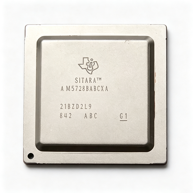
AM5728BABCXA - Dual Cortex-A15 1.5GHz Sitara MPU | Texas Instruments
The Texas Instruments AM5728BABCXA is a Sitara microprocessor (MPU/SoC) integrating dual ARM Cortex-A15 cores at up to 1.5 GHz, dual C66x floating-point DSP cores, and a PowerVR SGX544 3D graphics accelerator, housed in a 760-ball FCBGA (ABC) package measuring 23x23 mm and rated from -40C to +105C for industrial environments. A microprocessor is a CPU integrated on a single chip that executes instructions and manages data flow in embedded computing systems. The AM5728 is a system-on-chip (SoC) that combines multiple heterogeneous processing cores (ARM and DSP) with memory controllers, peripheral interfaces, and graphics acceleration, forming the computational heart of an embedded system. It sits within the hierarchy: SoC -> microprocessor -> embedded processor -> integrated circuit. Key features include dual 1.5 GHz ARM Cortex-A15 cores for general-purpose OS workloads, dual C66x DSP cores for math-intensive signal processing, a dual-core PRU-ICSS for deterministic real-time industrial Ethernet protocols, DDR3/DDR3L memory support, HDMI and LCD display interfaces, and Gigabit Ethernet, USB 3.0, PCIe, and SATA connectivity. An integrated video acceleration engine handles H.264 encode/decode for multimedia pipelines. Architecturally, the AM5728 uses a heterogeneous multicore design supporting asymmetric (AMP) or symmetric (SMP) multiprocessing. ARM cores run Linux or RTOS workloads while DSP cores offload computationally heavy tasks; the PRU-ICSS provides deterministic low-latency I/O, optimizing performance per watt across diverse workloads. The 760-FCBGA (23x23) 0.8 mm-pitch ball grid array supports high gate density with strong signal integrity for high-speed DDR and SerDes interfaces. Typical applications include industrial PLCs, medical ultrasound systems, human-machine interfaces (HMI), smart grid gateways, and non-safety automotive infotainment - anywhere edge computing requires local processing plus rich connectivity. When designing with this device, ensure adequate multi-rail power delivery and thermal management, following the TI datasheet power-sequencing and decoupling recommendations for reliable operation across the full -40C to +105C industrial range. This page synthesizes distributor availability, drop-in alternatives from the AM57x family, and practical design notes not found in the manufacturer datasheet.
AM6528 Sitara MPU Dual Cortex-A53 + R5F 1.1GHz | TI
The Texas Instruments AM6528 is a Sitara applications processor featuring dual Arm Cortex-A53 cores running up to 1.1 GHz, dual lockstep-capable Arm Cortex-R5F cores at 400 MHz, a Gigabit PRU-ICSS for industrial Ethernet protocols, and integrated 3D graphics acceleration (SGX544). The AM6528BACDXEA variant ships in a 784-ball FCBGA package measuring 23x23 mm. An applications processor (MPU) is a high-performance system-on-chip designed to run a full operating system such as Linux, in contrast to microcontrollers (MCUs) that execute bare-metal or RTOS code. Within the embedded hierarchy, the AM6528 sits at: MPU -> applications processor -> embedded processor -> semiconductor, and occupies the mid-tier of TI's Sitara AM65x family between single-A53 parts and the quad-core AM6548. Key differentiating features include the heterogeneous dual Cortex-A53 + dual Cortex-R5F architecture, which lets Linux handle HMI, networking and connectivity while the R5F cores manage deterministic real-time control. The Gigabit PRU-ICSS offloads industrial protocols such as EtherCAT, PROFINET and EtherNet/IP from the main Arm cores, and the integrated 3D GPU enables graphics-rich HMI panels without an external display processor. The AM65x platform is built to meet the complex processing needs of Industry 4.0 embedded products, per TI's AM654x/AM652x datasheet (SPRSP52C, revised September 2023). Silicon revision 2.1 devices are currently shipping. TI's compare tool positions the AM6528 against the AM6548 and AM6442, with industrial communication software stacks and up to 5 Gigabit Ethernet ports available across the family. Typical applications include industrial HMI panels, PLCs, edge gateways, and motor-drive control systems where real-time determinism and Linux-level connectivity must coexist on a single silicon platform. Design consideration: the 784-FCBGA package demands careful PCB stackup planning; use TI reference designs such as the AM65x GP EVM for power sequencing, DDR4 routing and BGA escape routing guidance. This page synthesizes verified distributor pricing, drop-in family alternatives, and practical design notes not found in the manufacturer datasheet.
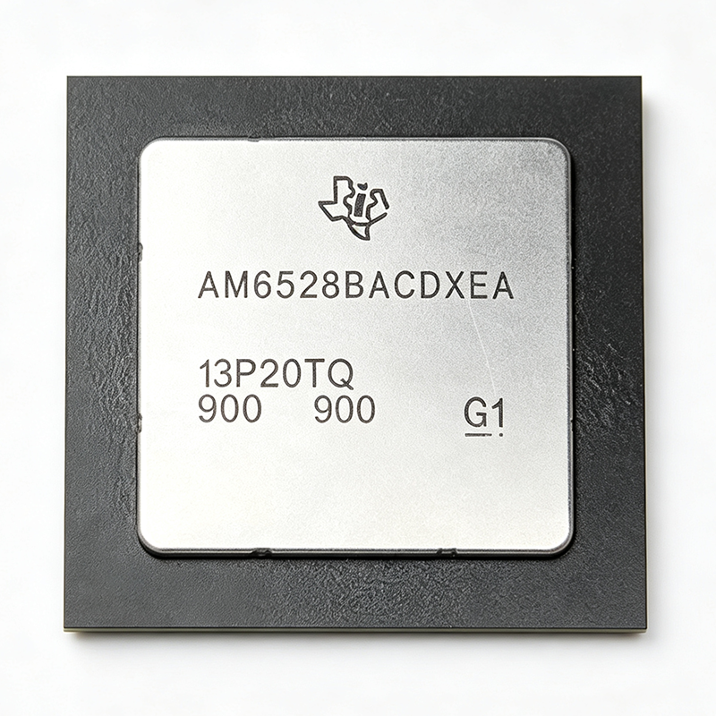
AM6528BACDXEA - Dual Cortex-A53 1.1GHz Sitara MPU | TI
The Texas Instruments AM6528BACDXEA is a Sitara microprocessor (MPU) integrating dual Arm Cortex-A53 cores running at 1.1 GHz, a dual Arm Cortex-R5F MCU subsystem at 400 MHz, and Gigabit-class PRU-ICSS industrial communication subsystems, housed in a 784-pin FCCSP (ACD) package measuring 23x23 mm and rated for -40C to +105C operation. A microprocessor unit (MPU) is the central computation engine of an embedded system, sitting above microcontrollers (MCU) in the processing hierarchy but below application processors in complexity. Modern industrial MPUs like the AM6528 combine an applications-class Arm Cortex-A53 cluster for Linux-based software with a real-time Cortex-R5F lockstep-capable MCU subsystem, enabling a single chip to run both a high-level OS and deterministic real-time control tasks - a partitioning that previously required two separate devices. Key differentiating features include the PRU-ICSSG (Programmable Real-time Unit Industrial Communication Subsystem) with three Gigabit instances, supporting industrial Ethernet protocols such as EtherCAT, PROFINET, and EtherNet/IP in hardware with deterministic latency. A 3D graphics acceleration engine (SGX544 class) enables HMI and visualization workloads. The Cortex-R5F subsystem includes features intended to support functional-safety goals per the TI datasheet for the AM654x/AM652x family (Silicon Revision 2.1 documentation). Architecturally, the AM6528 belongs to the Sitara AM65x generation, built on TI's proven Cortex-A53/R5F heterogeneous multicore approach. The A53 cluster executes Linux or RTOS software, while the R5F cores handle time-critical control loops and safety monitoring, communicating through shared on-chip interconnect and memory subsystems. Typical applications include industrial PLCs and motor drive control heads, factory automation gateways with multi-protocol industrial Ethernet, HMI panels with 3D graphics, and building/energy automation controllers where -40C to +105C operation is required. When designing with this part, plan power sequencing for the multiple core rails and allocate DDR memory bandwidth carefully between the A53 and R5F subsystems; TI provides reference designs and power estimation tools in the AM65x documentation set. This page synthesizes distributor pricing, same-family drop-in alternatives, and practical design notes not found in the manufacturer datasheet.
ATMEGA328P-AU - 8-bit AVR MCU 20MHz 32KB Flash | Microchip
The Microchip Technology ATMEGA328P-AU is a high-performance, low-power 8-bit AVR RISC microcontroller executing up to 20 MIPS at 20 MHz. It integrates 32 KB of in-system programmable FLASH, 1 KB EEPROM, and 2 KB SRAM in a 32-pin TQFP (7x7 mm, 0.8 mm pitch) package with 23 programmable I/O lines. An 8-bit microcontroller is a single-chip computer combining an 8-bit CPU, program memory, data memory, and peripherals on one die. Within the power-management and embedded-system hierarchy, MCUs sit at the top of the control chain, orchestrating sensors, actuators, and communication interfaces. The AVR architecture uses a Harvard organization with separate program and data buses, enabling most instructions to execute in a single clock cycle for deterministic, real-time behavior. Key features include picoPower technology with six sleep modes (down to 0.2 uA typical in Power-down), a wide 1.8V to 5.5V operating voltage, two 8-bit timers plus one 16-bit timer, six PWM channels, an 8-channel 10-bit ADC, and USART, SPI, and I2C serial interfaces. A programmable watchdog timer with its own on-chip oscillator, an analog comparator, and an on-chip temperature sensor round out the peripheral set. Technical depth: the device supports In-System Programming (ISP) via SPI and includes the debugWIRE on-chip debug system, reducing external debug hardware to a single wire. The high-density non-volatile memory process guarantees 10,000 FLASH write/erase cycles and 20-year data retention (per Atmel/Microchip AVR family datasheet). Typical applications include Arduino Uno and Nano boards, IoT sensor nodes, motor control, consumer appliances, and educational platforms. The -AU suffix denotes the industrial-grade (-40C to +85C) TQFP-32 package variant. Design tip: place 100 nF decoupling capacitors close to VCC and AVCC; use the internal 8 MHz RC oscillator for cost-sensitive designs or an external crystal for UART-critical accuracy. Prices below are as of 2026-08-29.
ATSAM4S2BB-MN - 120MHz Cortex-M4 128KB Flash 64-QFN | Microchip
The Microchip Technology ATSAM4S2BB-MN is a high-performance 32-bit microcontroller built on the ARM Cortex-M4 core with DSP instructions and Thumb-2 instruction set, operating at up to 120 MHz. It integrates 128 KB of embedded Flash with ECC, security bit and lock bits, plus 64 KB of SRAM, in a 64-pin QFN (9x9 mm) package with exposed pad and extended industrial temperature range. A microcontroller (MCU) is a compact integrated circuit that governs specific operations in embedded systems, containing a processor core, memory, and programmable peripherals. The ARM Cortex-M4 is a 32-bit RISC core with a hardware FPU and DSP instructions; the SAM4S series belongs to Microchip's SAM4 family of low-power, high-performance ARM-based MCUs. Key features include a 1.62V to 3.6V supply range, 180 uA low-power mode consumption, a rich peripheral set (multiple UARTs, SPI, I2C/TWI, USB, 12-bit ADC), and a Memory Protection Unit (MPU) for reliability. Flash ECC detects and corrects single-bit errors, improving data integrity in critical applications. Technically, the Cortex-M4 pipeline delivers 1.25 DMIPS/MHz-class performance, and the internal voltage regulator generates the stable core supply. The device is pin-to-pin compatible with SAM3S, SAM4N, and SAM7S legacy products in the 64-pin version, enabling easy migration from older designs without PCB rework. Typical applications include industrial control systems, medical devices, consumer electronics, and IoT endpoints where real-time processing, connectivity, and battery efficiency matter. It is supported by Microchip MPLAB X IDE, the Harmony software framework, and standard ARM toolchains for rapid development. Design tip: decouple all power pins with 100 nF capacitors placed close to the device, solder the exposed pad to a PCB thermal pad for heat dissipation, and follow datasheet layout guidelines to minimize noise.
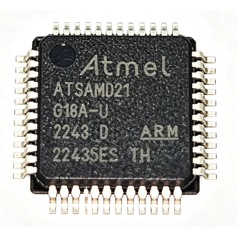
ATSAMD21G18A-AU - 48MHz Cortex-M0+ MCU 256KB Flash | Microchip
The Microchip Technology ATSAMD21G18A-AU is a low-power, high-performance 32-bit microcontroller based on the ARM Cortex-M0+ processor. It operates at up to 48 MHz and features 256 KB of flash memory and 32 KB of SRAM, making it suitable for a wide range of applications including home automation, consumer electronics, metering, and industrial control. The device is offered in a 48-pin TQFP (7x7 mm) package, providing a compact footprint for space-constrained designs. A microcontroller (MCU) is a compact integrated circuit designed to govern a specific operation in an embedded system. It contains a processor core, memory, and programmable input/output peripherals. The ARM Cortex-M0+ is an energy-efficient 32-bit processor core designed for low-cost and low-power embedded applications. The ATSAMD21G18A-AU belongs to the SAM D21 family, part of Microchip's SMART ARM-based microcontroller portfolio within the broader hierarchy of embedded processors. Key features include a 12-channel Direct Memory Access Controller (DMAC), a 12-channel Event System for inter-peripheral signaling, up to five 16-bit Timer/Counters (TC), and support for capacitive touch buttons, sliders, and wheels. It also includes a two-pin Serial Wire Debug (SWD) interface for programming and debugging, and is drop-in compatible with the SAM D20 series. Idle and standby sleep modes with SleepWalking peripherals enable low-power operation. The device integrates multiple SERCOM serial interfaces configurable as USART, SPI, or I2C, a 12-bit ADC, and a DAC. The Event System allows peripherals to communicate without CPU intervention, reducing power consumption and improving system efficiency. Supply voltage range is 1.62V to 3.63V, reaching 2.46 CoreMark/MHz. The MCU is functional-safety (FuSa) ready per Microchip's documentation and is RoHS-compliant (green package). Typical applications include home automation controllers, smart meters, industrial sensors, and consumer devices such as wearables and IoT nodes. The ATSAMD21G18A-AU is widely used in Arduino-compatible boards like the Arduino Zero and MKR series, making it popular for prototyping and education. Its low-power modes and rich peripheral set make it ideal for battery-powered designs. When designing with this MCU, decouple all VDD pins with 100nF capacitors placed close to each pin and add a 10uF bulk capacitor on the main supply. Bring the SWD interface out to a header for programming and debugging. For low-power designs, use standby sleep mode and configure the Event System to wake the device on peripheral events.

ATSAMD21J18A-AUT - 48MHz Cortex-M0+ MCU 256KB Flash TQFP-64 | Microchip
The Microchip ATSAMD21J18A-AUT (the complete device carrying the -AUT ordering suffix) is a 32-bit ARM Cortex-M0+ functional-safety (FuSa) microcontroller operating at up to 48 MHz, with 256KB FLASH and a 64-pin TQFP (10x10 mm) package. The -AUT suffix denotes the extended automotive operating temperature variant of the SAM D21J family. A microcontroller (MCU) is a single-chip computer that integrates a processor core, memory (FLASH for code, SRAM for data) and peripherals such as timers, serial interfaces and ADCs onto one die. MCUs sit at the top of the embedded hierarchy: silicon die -> ARM Cortex-M0+ 32-bit core -> SAM D21 product family -> ATSAMD21J18A device. The SAM D21 series (formerly Atmel | SMART) delivers up to 2.46 CoreMark/MHz efficiency at a 48 MHz maximum frequency, as stated by Atmel/Microchip product documentation. Key features of this part include the 256KB (256K x 8) FLASH memory, ARM Cortex-M0+ core running at 48 MHz, functional-safety qualification, and the 64-TQFP surface-mount package that provides a large general-purpose I/O count suitable for complex boards. The J-series pin count (64 pins) offers more ports than the G (48-pin) and E (32-pin) variants within the same family, letting designs scale memory and I/O without changing toolchains. Architecturally, the Cortex-M0+ is ARM's most energy-efficient 32-bit core, using a 2-stage pipeline and Thumb-2 instruction subset. Microchip's SAM D21 implementation targets low-power embedded control with CoreMark/MHz efficiency of 2.46, competing directly against STMicroelectronics' STM32 Cortex-M family in cost-sensitive designs. Typical applications include automotive auxiliary and body modules exposed to extended temperatures, industrial sensors and actuators, and IoT/connected devices requiring a small, efficient 32-bit core. Design consideration: confirm the -AUT temperature range and FLASH density suffix exactly when ordering, because the same die ships in many speed/memory/package combinations. This page synthesizes distributor listings, verified datasheet data, drop-in family alternatives, and practical design notes not found in a single manufacturer datasheet.
ATSAMV71N20B-CBT - 300MHz Cortex-M7 MCU 1MB Flash | Microchip
The Microchip ATSAMV71N20B-CBT is an automotive-grade 32-bit microcontroller based on the ARM Cortex-M7 core with double-precision FPU, running at up to 300MHz with 1MB (1M x 8) embedded Flash and 384KB SRAM, supplied in a 100-ball TFBGA (9x9 mm) package. Per Microchip, the SAM V71 family is manufactured under ISO-TS-16949 requirements and qualified to AEC-Q100 for automotive applications. A microcontroller (MCU) is a single-chip embedded processor that integrates a CPU core, memory, and peripherals into one device, forming the highest-volume class of embedded processing ICs used across automotive, industrial, and consumer systems. The SAM V71 sits at the high-performance end of the MCU hierarchy, positioned above general-purpose Cortex-M4 devices by its superscalar Cortex-M7 pipeline delivering 5.04 CoreMark/MHz. Key features include a 300MHz core with cache acceleration, dual 16-bit 2Msps ADCs, Ethernet MAC with AVB support for automotive audio-video bridging, dual CAN interfaces, I2S for digital audio, USB high-speed device/host, and multiple USART/SPI/TWI peripherals. The LCD controller-capable parallel capture interface and SDRAM/SDIO support enable graphics and data-logging designs. Architecturally, the Cortex-M7 core pairs a six-stage dual-issue pipeline with tightly-coupled memory (TCM) and configurable instruction/data caches, allowing deterministic execution for motor control and audio DSP workloads. The double-precision FPU accelerates control-loop math, while embedded Flash with ECC supports functional-safety-oriented designs. Typical applications include automotive gateway and body controllers, industrial automation and motor control, and Ethernet AVB audio/video networking. The combination of 300MHz throughput, hardware Ethernet, and dual CAN makes it a strong single-chip solution for connected embedded nodes. Design consideration: ensure a clean 3V to 3.6V supply with proper decoupling at all VDDIO/VDDCORE pins, and verify BGA escape-routing capability before committing to the 100-TFBGA footprint; pricing shown as of 2026-08-29.
ATTINY2313V-10PU - 8-bit AVR MCU 2KB Flash 10MHz | Microchip
The Microchip ATTINY2313V-10PU is a low-power, high-performance 8-bit AVR RISC-based microcontroller featuring 2KB of In-System Programmable Flash memory, 128 bytes of EEPROM, and 128 bytes of internal SRAM. Housed in a 20-pin PDIP package, this device operates at a maximum clock frequency of 10MHz and supports a supply voltage range of 1.8V to 5.5V, making it suitable for battery-powered and low-voltage applications. An 8-bit microcontroller is a compact integrated circuit that contains a processor core, memory, and programmable input/output peripherals on a single chip. The AVR architecture, developed by Atmel (now Microchip), uses an enhanced RISC instruction set that executes most instructions in a single clock cycle, achieving throughputs approaching 1 MIPS per MHz. This efficiency allows designers to optimize power consumption versus processing speed, a critical consideration in embedded systems. Key features of the ATTINY2313V-10PU include a universal serial interface (USI) that supports SPI and I2C communication, a full-duplex UART for serial communication, and debugWIRE for on-chip debugging. The device also includes a 16-bit timer/counter with PWM capabilities, an 8-bit timer/counter, an analog comparator, and up to 18 programmable I/O lines. The In-System Programmable Flash allows firmware updates via an SPI interface or a conventional programmer, simplifying development and field updates. Technically, the ATTINY2313V-10PU is manufactured using Atmel's high-density non-volatile memory technology. The low-voltage 'V' variant is optimized for operation down to 1.8V, making it ideal for portable devices. The device supports a wide operating temperature range of -40C to +85C, ensuring reliability in industrial environments. Its 20-pin PDIP package is through-hole mounted, which is convenient for prototyping and educational projects. Typical applications include sensor interfaces, motor control, LED lighting control, and small automation systems. The combination of low power consumption, versatile communication interfaces, and sufficient memory makes it a popular choice for hobbyist and professional embedded designs. When designing with this microcontroller, ensure proper decoupling capacitors on the power supply pins and consider using the internal oscillator to reduce external component count. The debugWIRE interface provides a cost-effective debugging solution without requiring additional pins.
AUT:A - ARM Cortex-M0+ MCU 128KB Flash 64TQFP | Microchip Technology
The Microchip Technology ATSAMD21J17A-AUT (site MPN key AUT:A) is a 32-bit ARM Cortex-M0+ microcontroller with 128KB Flash, 16KB SRAM, and a 48MHz maximum CPU clock, housed in a 64-pin TQFP (10x10 mm) package and rated for the industrial temperature range with a 1.6V to 3.6V supply. A microcontroller (MCU) is a single-chip computer that integrates a processor core, nonvolatile program memory (Flash), volatile data memory (SRAM), and peripheral interfaces such as USB, DMA controllers, timers, and serial communication blocks on one die. MCUs sit at the lowest level of the embedded-system hierarchy - below SoCs and application processors - and are the standard building blocks of industrial control boards, sensor nodes, and human-machine interfaces. Key features of this SAM D21 family device include the ARM Cortex-M0+ core with 2-stage pipeline and single-cycle I/O port access, a native USB 2.0 device interface, a multi-channel DMA controller that offloads data movement from the CPU, and hardware event system routing that allows peripherals to communicate without CPU intervention. The 128KB Flash supports in-system programming via SWD, and the device is offered in a green, RoHS-aligned TQFP package with Tape & Reel packing for automated assembly. Architecturally, the SAM D21 family implements a Harvard-architecture Cortex-M0+ running at up to 48MHz from an internal or external clock source, with sleep modes down to microamp level for battery designs. The J-pin-count variant (64 pins) provides the largest GPIO and peripheral complement in the family, including multiple SERCOM modules configurable as UART, SPI, or I2C. Typical applications include industrial automation controllers, USB-enabled sensor interfaces, motor control front-ends, and portable instrumentation where a 3.3V, 48MHz MCU with USB and DMA is required. Design consideration: the 1.6V to 3.6V supply range means a 3.3V rail is standard; ensure decoupling per the manufacturer datasheet and verify Flash endurance and clock configuration for your operating temperature. This page synthesizes distributor sourcing data, family-level drop-in alternatives, and structured specifications not consolidated in a single manufacturer datasheet view.
DSPIC33AK256MC506-E/M7 - 200MHz DSC FPU | Microchip
The Microchip Technology DSPIC33AK256MC506-E/M7 is a high-performance 32-bit Digital Signal Controller (DSC) from the dsPIC33A family, operating at 200 MHz with an integrated 32/64-bit Floating-Point Unit (FPU). It provides 256KB Flash program memory, 64KB SRAM, and is housed in a 64-VQFN (9x9 mm) package with extended temperature range of -40C to +125C. A Digital Signal Controller (DSC) combines the processing power of a digital signal processor (DSP) with the versatility of a microcontroller (MCU). DSCs are embedded processors positioned between general-purpose MCUs and high-end DSPs, designed for real-time control applications requiring intensive mathematical computation such as motor control, digital power conversion, and advanced sensing. Key features include high-speed 40 MSPS 12-bit ADCs, high-bandwidth 100 MHz op amps with low input voltage offset, high-speed PWMs, CAN-FD connectivity, and capacitive touch sensing. The device is functional safety (FuSa) compliant, supporting safety-oriented designs. The FPU accelerates single- and double-precision floating-point arithmetic, which is critical for control loop algorithms executing at high sample rates. Architecturally, the dsPIC33A core is a single-core 32-bit design with a DSP engine supporting MAC operations, delivering deterministic real-time performance. The rich peripheral set includes multiple UART, SPI, I2C, CAN-FD modules, analog comparators, and a 12-bit DAC. The high-speed ADC and PWM peripherals form an ideal pair for tightly coupled real-time control loops in digital power and motor drive systems. Typical applications include motor control (PMSM, BLDC, stepper), digital power conversion (SMPS, PFC, inverters), battery management systems, industrial automation, and advanced current, voltage, and temperature sensing. The 40 MSPS ADC and 100 MHz op amps enable precise signal acquisition without external analog front-end components. Design tip: properly decouple all VDD pins and use the internal regulator for the core voltage. Use the multiple PGECx/PGEDx pin pairs for in-circuit serial programming (ICSP), and leverage the built-in self-test and ECC features for functional safety compliance. Pricing as of 2026-08-29.
ESP32-P4NRW16X - Dual-Core RISC-V MCU, 16MB PSRAM | Espressif
The Espressif Systems ESP32-P4NRW16X is a 32-bit high-performance microcontroller (MCU) SoC with a RISC-V dual-core high-performance (HP) microprocessor at up to 400 MHz-class performance, a single-core low-power (LP) microprocessor, and 16 MB of in-package PSRAM (OPI/HPI) in a 10 x 10 mm QFN-104 package. A microcontroller SoC integrates a processor core, memory, and peripherals on a single chip, sitting at the top of the embedded hierarchy: MCU -> system-on-chip (SoC) -> embedded system. The ESP32-P4 family extends the ESP32 product line by removing on-chip Wi-Fi/Bluetooth radio and instead focusing on compute, memory, and display/vision peripherals, pairing naturally with Espressif companion connectivity chips such as the ESP32-C6. Key features include the HP/LP dual-system architecture, where the LP single-core RISC-V processor keeps monitoring and wake-up tasks running while the HP cores sleep; 16 MB of in-package OPI/HPI PSRAM with a 1.8 V VDD_PSRAM rail; dedicated MIPI CSI and MIPI DSI interfaces for camera input and display output; and an industrial ambient temperature range of -40 to +85 C. Technically, the ESP32-P4 is built for rich HMI, edge computing, image processing, and voice processing. The HP system contains the dual-core RISC-V microprocessor with access to large internal memory, while hardware accelerated image and voice paths offload the CPU. Espressif recommends the v3.0-or-later reference schematic and at least a 4-layer PCB for new designs, and the series is currently supplied at chip revision v3.x. Typical applications include smart display HMI panels with MIPI DSI screens, camera/vision nodes using MIPI CSI image sensors, and voice-assistant endpoints with on-device audio processing. Paired with an ESP32-C6 for Wi-Fi 6 and 802.15.4, the P4 forms the compute engine of a modern connected HMI. Design consideration: because the in-package PSRAM operates at 1.8 V (VDD_PSRAM_0/1), power-rail sequencing and the recommended 4-layer stackup with solid ground planes are critical for signal integrity on the OPI PSRAM and MIPI buses. This page synthesizes distributor pricing, drop-in alternatives within the ESP32-P4 family, and practical design notes not found in the manufacturer datasheet.
ESP32-P4NRW32X - Dual-Core RISC-V HMI MCU 32MB PSRAM | Espressif
The Espressif Systems ESP32-P4NRW32X is a high-performance 32-bit microcontroller built around a dual-core RISC-V HP (high-performance) processor plus a single-core RISC-V LP (low-power) coprocessor, with 32 MB of in-package PSRAM, housed in a 104-pin QFN package measuring 10 x 10 mm. A microcontroller (MCU) is a single integrated circuit that combines a processor core, memory, and programmable peripherals into one chip, sitting at the heart of the embedded systems hierarchy: SoC -> microcontroller -> embedded system. The ESP32-P4 is Espressif's flagship application-class MCU, positioned above the ESP32-S3 for compute-intensive embedded workloads. Key features include the HP/LP dual-system architecture that lets the LP core handle sleep-state housekeeping while the HP cores run demanding workloads, 32 MB of in-package PSRAM (the NRW32 variant) supporting large frame buffers, powerful image and voice processing capability, and rich HMI-oriented peripherals. Unlike most ESP32 family members, the ESP32-P4 focuses purely on compute; wireless connectivity is added externally via companion chips such as the ESP32-C6. Technically, the HP system contains the dual-core RISC-V processor with AI instruction extensions, an advanced memory subsystem, and integrated high-speed peripherals, while the LP system contains the single-core RISC-V low-power microprocessor. This split allows always-on voice wake-word detection or sensor polling at minimal power, waking the HP cores only when needed. Typical applications include rich Human-Machine Interfaces (HMI) with touch displays, edge computing nodes, image and camera processing pipelines, and voice processing endpoints. The large in-package PSRAM directly supports display frame buffers and AI model working sets without external memory routing. Design consideration: Espressif recommends the v3-or-later reference schematic for new designs and at least a 4-layer PCB for the 10 x 10 mm QFN-104 footprint; strapping pins must be reviewed against the ESP32-P4 datasheet before layout is frozen. This page synthesizes distributor pricing, drop-in alternatives, package guidance, and design notes not found in the manufacturer datasheet.

F28027PTT - 60MHz C28x Piccolo MCU, 64KB Flash | Texas Instruments
The Texas Instruments F28027PTT (also known as TMS320F28027PTT) is a 32-bit C2000 Piccolo microcontroller built around the C28x core, operating at up to 60 MHz. It features 64KB (32K x 16) of flash memory and is housed in a 48-pin LQFP (PT) package measuring 7x7 mm. This device is designed for real-time control applications, offering a high level of analog integration and an internal voltage regulator for single-rail operation. A microcontroller (MCU) is a compact integrated circuit that combines a processor core, memory, and programmable input/output peripherals on a single chip. The C28x core is a 32-bit fixed-point DSP-optimized architecture from Texas Instruments, specifically engineered for real-time control tasks. It sits within the C2000 family, which is a subset of microcontrollers tailored for industrial and automotive control systems, such as motor drives, power conversion, and digital power supplies. The C28x core excels at executing control algorithms with high precision and low latency, making it a preferred choice for closed-loop systems. Key features of the F28027PTT include a 60 MHz clock speed, 64KB flash memory, and a rich set of control peripherals. It integrates a 12-bit ADC, multiple PWM channels, and communication interfaces like SPI, SCI (UART), and I2C. The device operates over a temperature range of -40°C to 105°C, making it suitable for harsh environments. The internal voltage regulator simplifies power supply design, allowing operation from a single 3.3V rail. Technically, the F28027PTT leverages the C28x core's Harvard architecture, which enables simultaneous instruction and data access, improving throughput. The flash memory supports on-chip programming, facilitating firmware updates in the field. The device also includes a boot ROM with factory-programmed bootloader routines, enabling flexible boot options from various interfaces. The analog-to-digital converter (ADC) offers 12-bit resolution with multiple sample-and-hold channels, crucial for precise sensor measurements in control loops. Typical applications include white goods (such as washing machines and refrigerators), switched-mode power supplies (SMPS), and DC-DC multiple-output power supplies. The F28027PTT's high-performance C28x core and integrated peripherals make it ideal for implementing complex control algorithms like field-oriented control (FOC) for motors and digital power conversion. Its low pin count and small package footprint also suit space-constrained designs. When designing with this device, ensure proper decoupling of the power supply pins and consider the thermal characteristics of the LQFP package. The internal voltage regulator requires an external capacitor for stability. Additionally, the ADC reference pins should be filtered to minimize noise, as this directly impacts measurement accuracy in control applications.
F29H859TU-Q1 - Automotive C2000 64-bit MCU | Texas Instruments
The Texas Instruments F29H859TU-Q1 is an automotive-grade C2000 real-time microcontroller featuring a 64-bit C29x CPU running at 200MHz with triple-core architecture and lockstep capability. It provides 4MB of flash memory and is designed for functional safety compliance in power electronics, motor control, and GaN/SiC-based applications. The C2000 family is a well-known series of ultra-low-latency MCUs optimized for real-time control. The F29H859TU-Q1 belongs to the F29H85x sub-family, which leverages the next-generation C29 CPU core to enable high power density and high switching frequency operation. This MCU is specifically qualified for automotive environments (Q1 suffix), meeting the stringent reliability and AEC-Q100 standards required in vehicles. Key features of the F29H859TU-Q1 include a triple-core 200MHz C29x CPU with lockstep mode for enhanced safety, 4MB flash memory, and functional safety compliance. The architecture supports advanced real-time control loops, making it suitable for applications like DC-DC converters, traction inverters, on-board chargers, and solar inverters. The F29H859TU-Q1 is available in a BGA package, which is the only practical packaging option for this high pin-count MCU as confirmed by TI support. The device is designed for surface mount assembly and operates across automotive temperature ranges, enabling compact and robust system designs. Typical applications include digital power supply control, motor control for electric vehicles, renewable energy inverters, and industrial automation systems. The high-performance CPU and large flash memory allow for complex algorithms and firmware updates, while the functional safety features ensure reliable operation in safety-critical systems. When designing with the F29H859TU-Q1, engineers should consider adequate thermal management and decoupling for high-speed digital switching. The C29x architecture requires careful attention to power supply stability and PCB layout to maximize performance and safety.