Microcontrollers
Products (422)
F29P329SM-Q1 - 200MHz C29 Auto MCU | Texas Instruments
The Texas Instruments F29P329SM-Q1 is an automotive-grade 64-bit C2000 real-time microcontroller featuring the next-generation C29 CPU running at 200 MHz. It integrates 2MB of flash memory and supports lockstep operation for functional safety compliance, making it suitable for ASIL-D / SIL-3 applications. The device comes in a 100-pin PZS package and operates over -40°C to +125°C. What is a C2000 real-time microcontroller? The C2000 family is a series of MCUs designed for real-time control applications such as motor control, power conversion, and digital power supplies. These MCUs feature a highly efficient CPU with low latency, integrated analog peripherals (ADCs, DACs, comparators), and enhanced PWM modules, enabling precise control loops. The C29 CPU is the latest generation, offering higher performance and advanced safety features. Key features include 200MHz operation, 2MB flash, lockstep with error detection, functional safety compliance (ISO 26262), and automotive AEC-Q100 qualification. The C29 core is a 64-bit architecture with 128-bit data paths, providing faster single-cycle access to memory. The device supports multiple communication interfaces such as CAN, UART, SPI, and I2C, though exact counts are not available from the provided data. Typical applications include automotive motor control (e.g., traction inverters), digital power supplies (e.g., LLC converters), vehicle electrification (battery management), industrial drives, and renewable energy inverters. The 200MHz clock and advanced PWM capabilities ensure high-precision control loops. When designing with this MCU, pay attention to power supply decoupling and thermal management. The 200MHz core can dissipate significant power; use multiple VDD pins with ceramic capacitors and consider thermal vias under the exposed pad. Also, use the lockstep fail-safe features to implement safe shutdown paths.
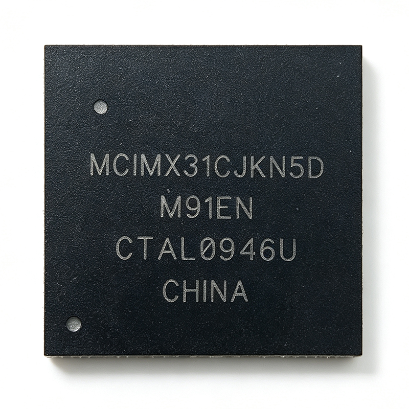
MCIMX31CJKN5D - i.MX31 532MHz ARM11 MPU | NXP
The NXP MCIMX31CJKN5D is an i.MX31 applications microprocessor based on the 32-bit ARM1136JF-S core, operating at 532 MHz in a 457-pin LFBGA (MAPBGA) package measuring 14 x 14 mm with 0.5 mm ball pitch. This single-core applications processor integrates the ARM11 CPU, vector floating point unit, and a rich peripheral set for consumer and industrial embedded systems. An applications processor (MPU) is a system-on-chip class device that, unlike a microcontroller, is designed to run full operating systems such as embedded Linux or Windows CE, offloading display, multimedia, and connectivity workloads. Within the power hierarchy of embedded processors - microcontroller -> applications processor -> SoC - the i.MX31 family sits in the mid-range segment that powered millions of consumer, industrial, automotive, and medical devices. Key features of the i.MX31 include the ARM1136JF-S core with VFP11 floating point coprocessor, integrated image processing for camera input, LCD controller support, USB, SD/MMC interfaces, and multiple power management modes. The 532 MHz clock frequency delivers sufficient headroom for H.264 baseline video decode and graphical user interfaces typical of its generation. Architecturally, the device combines the ARM11 core with NXP smart speed technology, multi-layer system bus fabric, and an external memory interface supporting DDR and mDDR SDRAM, NOR/NAND flash, and PCMCIA. Power supply operation is centered around 1.65 V core domains per supplier data, with sophisticated clock gating for low standby power. Typical applications include industrial HMI panels, portable medical monitors, consumer multimedia devices, and general embedded control where a legacy i.MX31 platform must be maintained. The 457-ball footprint supports dense two-sided PCB layouts. Design consideration: this part is listed by NXP as End of Life, so new designs should select a current i.MX generation such as i.MX 8M, while existing designs should secure stock or qualify the pin-compatible family variants listed below. Prices shown are as of 2026-08-29.
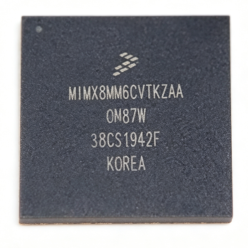
MIMX8MM6CVTKZAA - i.MX8MM Quad A53 1.6GHz SoC | NXP
The NXP Semiconductors MIMX8MM6CVTKZAA is a high-performance embedded applications processor from the i.MX 8M Mini family, built on advanced 14LPC FinFET process technology. It integrates a quad-core ARM Cortex-A53 application processor running at up to 1.6GHz along with a Cortex-M4F core for real-time processing, housed in a 486-ball LFBGA package (14x14 mm) for industrial and consumer applications balancing performance, power efficiency, and multimedia capabilities. An applications processor is a system-on-chip (SoC) designed to run operating systems such as embedded Linux and complex application software on ARM architecture. It integrates CPU cores, memory controllers, graphics, and I/O interfaces, serving as the main processing unit in smart home hubs, IoT gateways, and industrial control systems. The i.MX 8M Mini sits between the lower-power i.MX 6 series and the higher-performance i.MX 8M Quad/Plus in the embedded processor hierarchy. Key features include the 64-bit quad-core Cortex-A53 cluster at 1.6GHz, a Cortex-M4F core for low-latency deterministic control, a 3D GPU (GC NanoUltra), a 2D GPU, and a 4K VPU for video encode/decode. Memory support covers LPDDR4/DDR4, and connectivity includes Gigabit Ethernet, USB 3.0, PCIe, and multiple display interfaces. Technically, the 14LPC FinFET process delivers improved power efficiency versus older planar nodes. The heterogeneous multicore architecture partitions tasks between the A53 cluster and the M4F core, enabling efficient power management. TrustZone support provides secure boot and secure execution for secure IoT deployments. Typical applications include smart home hubs, IoT gateways, industrial HMI, medical devices, and multimedia streaming devices, where combined CPU, GPU, VPU, and connectivity resources suit edge computing and AI inference. Design tip: pay careful attention to power sequencing and thermal management. The 486-ball LFBGA requires a multi-layer PCB with thermal vias and a solid ground plane, plus proper decoupling capacitors near power pins for stable operation.

MIMX8QM5CVUFFAB - i.MX 8QuadMax 8-Core SoC | NXP | 1313-BGA
The NXP Semiconductors MIMX8QM5CVUFFAB is the i.MX 8QuadMax application processor, a heterogeneous eight-core System on Chip (SoC) integrating two Arm Cortex-A72, four Arm Cortex-A53, and two Arm Cortex-M4F cores in a 1313-ball FBGA package measuring 29x29 mm with automotive temperature grade. An SoC (System on Chip) consolidates CPU, GPU, memory interfaces, and peripheral controllers into a single integrated circuit, forming the complete computing heart of an embedded system. The i.MX 8QuadMax sits at the top of the NXP i.MX 8 family (alongside 8QuadPlus and 8DualMax), targeting high-performance automotive, industrial, and consumer platforms that need advanced graphics, vision processing, and deterministic real-time control in one device. Key features include full-chip hardware virtualization with domain protection for secure multi-OS operation, independent graphics across four HD displays or one 4K screen, an integrated vision pipeline for ADAS-class perception, and an audio subsystem optimized for voice and speech recognition. The dual Cortex-A72 cores handle heavy application workloads, the quad Cortex-A53 cores provide power-efficient scaling, and the dual Cortex-M4F cores run real-time, safety-relevant tasks - a heterogeneous balance of throughput and efficiency. The architecture supports Android, Linux, FreeRTOS, QNX, Green Hills, and Dornerworks XEN operating systems, and the family offers pin- and power-compatible packages for hardware design reuse. Typical applications include automotive digital cockpits, infotainment, ADAS vision systems, industrial HMI panels, and medical imaging equipment, where rich UI and real-time control must coexist. Design consideration: the 1313-ball BGA demands a multi-layer PCB with thermal vias and strict power sequencing; the MSL 3 rating (168-hour floor life) requires controlled moisture handling before reflow.
MPC5741PK1AMLQ8R - Dual-Core 180MHz 1MB MCU | NXP
The NXP MPC5741PK1AMLQ8R is a 32-bit dual-core microcontroller from the MPC57xx family, featuring two Power Architecture e200z4 cores running at 180 MHz, 1MB of flash memory (1M x 8), and 128KB of SRAM in a 144-pin LQFP (20x20 mm) surface-mount package. The device supports CANbus, Ethernet, FlexRay, LINbus, SPI, and UART/USART connectivity, making it a connectivity-rich hub for real-time embedded control. A microcontroller (MCU) is a compact integrated circuit that combines a processor core, memory, and programmable peripherals on a single die to govern a specific operation in an embedded system. The MPC5741PK1AMLQ8R is a 32-bit MCU, processing data in 32-bit chunks for higher performance and precision than 8-bit or 16-bit parts. It belongs to the MPC57xx family within NXP's automotive-grade microcontroller portfolio; per NXP documentation, MPC5741P-class devices are suitable for ISO 26262 ASIL-D chassis and safety applications, positioning them high in the vehicle functional-safety hierarchy. Key features include the dual e200z4 cores enabling task partitioning between application and safety monitoring functions, 4x ADC modules for precise analog acquisition, 2x PWM modules for motor and power control, and 2x SENT interfaces for automotive sensor connectivity. These peripherals directly address the needs of engine management and chassis systems that must interleave control loops with safety diagnostics. Technically, the e200z4 Power Architecture core is optimized for deterministic real-time execution, and the dual-core lockstep-capable architecture enhances reliability in safety-critical systems. The device operates from a 3.3V supply over a -40C to +125C automotive temperature range. Typical applications include automotive engine control units (ECUs), transmission control, ADAS domain control, chassis and safety systems, and industrial automation requiring deterministic real-time control. Design consideration: properly decouple the 3.3V supply and account for thermal dissipation at 180 MHz operation; use the integrated low-power modes to optimize energy efficiency in battery-connected systems. Pricing shown is [DATA_NEEDED: current unit pricing] as of 2026-08-29.

MPC5777C - 264MHz Dual-Core Power Architecture MCU | NXP
The NXP MPC5777C is a high-performance 32-bit automotive microcontroller built on Power Architecture technology, targeting advanced engine control, functional safety, and security applications. It integrates a dual-core e200z7 processor cluster running at up to 264 MHz with lockstep capability, plus an auxiliary e200z0 core for peripheral and safety processing, and offers up to 8 MB of flash memory and 768 KB of SRAM. A microcontroller (MCU) is a compact integrated circuit that governs a specific operation in an embedded system, combining a processor core, memory, and programmable I/O peripherals on one die. The MPC5777C belongs to the automotive MCU family within the broader embedded processor hierarchy, alongside DSPs and SoCs, and is specifically engineered for harsh, real-time, safety-critical environments such as under-hood powertrain control. Key features include lockstep dual cores supporting ASIL-D (ISO 26262) and SIL-1 (IEC 61508) functional safety, a hardware security module (CSE with encryption and tamper detection) for secure boot and communication, ECC on both flash and SRAM, and a memory protection unit. Comprehensive connectivity covers CAN, LIN, FlexRay, and Ethernet, while high-resolution eMIOS PWM timers and multiple ADCs support precision motor and engine control. Technically, the device is AEC-Q100 qualified and operates from -40C to +150C, ensuring reliability in demanding automotive thermal environments. NXP documents the family in the MPC5777C Data Sheet (Document Number MPC5777C Rev. 15, 03/2021) and the MPC5777C Reference Manual. Typical applications include engine control units (ECUs), transmission control, hybrid and electric vehicle powertrain/inverter control, and industrial motor drives where deterministic real-time loops and functional safety are mandatory. Design consideration: the MCU requires multiple supply rails (3.3V and 5V) with careful decoupling and a robust power sequencing scheme; at 264 MHz it can dissipate significant power, so thermal design with adequate copper pour on the MAPBGA land pattern is essential.

MSP430F1491 - 8MHz 16-bit MCU, 60KB Flash 64-LQFP | TI
The Texas Instruments MSP430F1491 is a 16-bit ultra-low-power mixed-signal microcontroller based on the MSP430 CPU16 RISC core, running at up to 8 MHz with 60KB Flash memory, 2KB SRAM, a 12-bit ADC, comparator, two USARTs (SPI/UART), and 48 I/O pins in a 64-pin LQFP (10x10 mm) package. An MCU (microcontroller unit) is a single-chip computer that integrates a processor core, program memory, data memory, and peripherals on one die. The MSP430 family occupies the ultra-low-power tier of the embedded processor hierarchy, sitting between general-purpose microcontrollers and dedicated ASSPs, and is designed for battery-operated and energy-harvesting systems where average current draw - not peak performance - is the dominant design constraint. Key features include an ultra-wide low supply range of 1.8 V to 3.6 V, active-mode consumption of just 280 uA at 1 MHz and 2.2 V, standby current of 1.6 uA, and RAM-retention off mode of 0.1 uA. Five software-selectable low-power modes (LPM0 through LPM4) and wakeup from standby in under 6 us allow aggressive duty-cycling that multiplies battery life by orders of magnitude versus always-on MCUs. Architecturally, the MSP430F1491 pairs a 16-bit RISC pipeline with an orthogonal instruction set and flash-based program memory with in-system programmability (ISP). Two built-in 16-bit timers (Timer_A and Timer_B) and a hardware multiplier accelerate math-intensive loops without CPU overhead. The two USARTs each function as asynchronous UART or synchronous SPI, and the 12-bit ADC with integrated sample-and-hold serves direct analog sensing. The F14x1 variant shares the MSP430F14x footprint, offering code- and hardware-compatible family scalability. Typical applications include battery-powered metering, portable instrumentation, sensor data loggers, and low-power industrial control nodes that need dual serial ports for connectivity plus the 12-bit ADC for analog channels. The 48 GPIOs support keypads, LCDs, and relay drive logic. Design consideration: budget memory carefully - 60KB Flash is ample for C-compiled firmware, but 2KB SRAM limits large buffers; use ring buffers and avoid heap fragmentation. This page synthesizes distributor data, same-family drop-in alternatives, and practical design notes beyond the manufacturer datasheet.
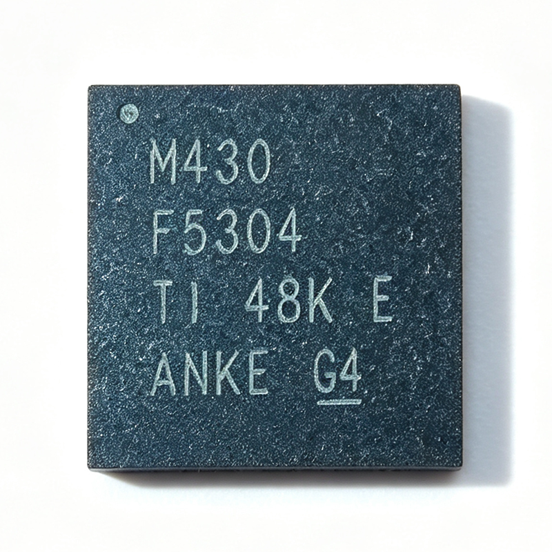
MSP430F5304IPTR - 16-bit 25MHz 8KB Flash MCU | Texas Instruments
The Texas Instruments MSP430F5304IPTR is a 16-bit ultra-low-power mixed-signal microcontroller based on the MSP430 CPUXV2 core, running at up to 25 MHz with 8KB Flash and 6KB SRAM in a 48-pin LQFP (7x7 mm) package. On-chip peripherals include an integrated 3.3V LDO, four 16-bit timers, a 10-bit ADC, one USCI (UART/SPI/I2C), a hardware multiplier, DMA, an RTC with alarm capabilities, and 31 I/O pins. An ultra-low-power microcontroller (MCU) is a single-chip processor optimized to minimize active and standby current draw, essential for battery-operated and energy-harvesting systems. The MSP430 family sits within the broader hierarchy of 16-bit microcontrollers -> mixed-signal MCUs -> embedded processors, and is widely recognized as an industry benchmark for low-power design. Key features include the flexible clock system (5 selectable low-power modes), a hardware 32x32 multiplier that offloads arithmetic from the CPU, and DMA for peripheral-to-memory transfers without CPU intervention. The integrated LDO simplifies power tree design by generating the core supply from a single external rail, while the RTC with alarm supports timekeeping during standby. The 10-bit ADC provides general-purpose analog acquisition for sensor front ends. The MSP430F5xx architecture pairs the von Neumann CPUXV2 core with a clock system supporting a VLO, REFO, XT1, and DCO sources, allowing designers to trade clock accuracy against current consumption. Interrupt-driven operation with fast wake-up keeps average current in the microamp range in duty-cycled applications. Typical applications include battery-powered metering, portable medical monitoring, industrial sensor nodes, and consumer appliances where the combination of 25 MHz performance, one USCI serial port, and 31 GPIO covers most moderate-complexity control tasks. Design consideration: the family shares the MSP430F5xx/F6xx User's Guide peripheral set, so code migrates freely between family members; verify Flash/SRAM sizing and package pinout before board reuse, as memory-density variants exist in identical footprints.
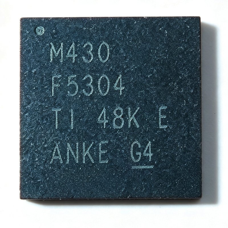
MSP430F5304IPTR - 16-bit 25MHz 8KB Flash MCU | Texas Instruments
The Texas Instruments MSP430F5304IPTR is a 16-bit ultra-low-power mixed-signal microcontroller based on the MSP430 CPUXV2 RISC core, running at up to 25 MHz with 8KB Flash and 6KB SRAM in a 48-pin LQFP (7x7 mm) package. On-chip peripherals include an integrated 3.3V LDO, four 16-bit timers, a high-performance 10-bit ADC, one USCI supporting UART/SPI/I2C, a hardware multiplier, DMA, an RTC with alarm capabilities, and 31 I/O pins. An ultra-low-power microcontroller (MCU) is a single-chip processor optimized to minimize active and standby current draw, essential for battery-operated and energy-harvesting systems. The MSP430 family sits within the broader hierarchy of 16-bit microcontrollers -> mixed-signal MCUs -> embedded processors, and is widely recognized as an industry benchmark for low-power design. Key features include the flexible clock system with five selectable low-power modes, a hardware 32x32 multiplier that offloads arithmetic from the CPU, and DMA for peripheral-to-memory transfers without CPU intervention. Active-mode consumption is approximately 195 uA/MHz at 8 MHz and 3V during Flash execution, with supply voltage supported from 2.4V to 3.6V. The MSP430F5xx architecture pairs the von Neumann CPUXV2 core with a clock system supporting VLO, REFO, XT1, and DCO sources, allowing designers to trade clock accuracy against current consumption. Interrupt-driven operation with fast wake-up keeps average current in the microamp range in duty-cycled applications. The integrated LDO simplifies the power tree by generating the core supply from a single external rail. Typical applications include battery-powered metering, portable medical monitoring, industrial sensor nodes, and consumer appliances where the combination of 25 MHz performance, one USCI serial port, and 31 GPIO covers most moderate-complexity control tasks. Design consideration: the family shares the MSP430F5xx/F6xx User's Guide peripheral set, so code migrates freely between family members; verify Flash/SRAM sizing and package pinout before board reuse, as memory-density variants exist in identical 48-LQFP footprints. This page synthesizes distributor pricing, drop-in alternatives, and practical design notes not found in the manufacturer datasheet, with data verified as of 2026-09-01.
MSP430F5529IPNR - 25MHz 128KB Flash USB MCU | Texas Instruments
The Texas Instruments MSP430F5529IPNR is a 16-bit ultra-low-power microcontroller featuring the MSP430 CPUXV2 core running at up to 25 MHz. It integrates 128KB of Flash memory, 8KB of SRAM, a 12-bit ADC, comparator, DMA, UART/SPI/I2C, USB 2.0, and a hardware multiplier, all in an 80-pin LQFP (PN) package measuring 12x12 mm. This device is part of the MSP430F55xx family, designed for extended battery life in portable and industrial applications. A microcontroller (MCU) is a compact integrated circuit containing a processor core, memory, and programmable input/output peripherals on a single chip. The MSP430 family is renowned for its ultra-low-power operation, featuring multiple low-power modes that reduce current consumption to microamps, making it ideal for battery-powered devices. The MSP430F5529IPNR sits within the MSP430F5xx series, which adds USB connectivity and enhanced analog peripherals while maintaining the low-power heritage of the MSP430 architecture. Key features include 25 MHz CPU speed, 128KB Flash, 8KB SRAM, a 12-bit ADC with up to 16 external channels, a comparator, DMA controller, two USCI modules supporting UART/SPI/I2C, a full-speed USB 2.0 interface with integrated PHY, and a 32-bit hardware multiplier. The device operates from 1.8V to 3.6V and supports a wide temperature range of -40C to +85C. The LQFP-80 package provides 63 I/O pins, enabling complex system integration. The MSP430F5529IPNR employs the MSP430 CPUXV2 architecture with a von-Neumann memory layout, offering efficient code density and low power consumption. The integrated USB module supports device, host, and OTG modes, simplifying connectivity in embedded systems. The hardware multiplier accelerates DSP-like operations, while the DMA controller offloads data transfers from the CPU, improving overall system throughput. Typical applications include portable medical devices, smart meters, industrial sensor nodes, USB-based data acquisition systems, and battery-powered IoT endpoints. The combination of low power, USB, and rich analog peripherals makes it a versatile choice for designs requiring extended battery life and connectivity. When designing with this MCU, pay attention to the power supply decoupling and the USB PHY layout to ensure signal integrity. The device supports multiple low-power modes, so configure the clock system and peripherals appropriately to maximize battery life.
MSP430FR2433IRGER - 16MHz FRAM MCU | TI
The Texas Instruments MSP430FR2433IRGER is a 16 MHz ultra-low-power 16-bit microcontroller based on the MSP430 CPU16 core, featuring 15.5KB FRAM, 4KB SRAM, a 10-bit ADC, UART/SPI/I2C, and timers, housed in a 24-pin VQFN (RGE) 4x4 mm package. A microcontroller (MCU) is a compact integrated circuit designed to govern a specific operation in an embedded system, containing a processor core, memory, and programmable input/output peripherals. Within the taxonomy, an MCU is an embedded processor and a type of integrated circuit. The MSP430 family is a 16-bit ultra-low-power microcontroller line known for extended battery life and is part of Texas Instruments' Value Line sensing portfolio. Key features of the MSP430FR2433IRGER include a 16 MHz CPU frequency, 15.5KB of ferroelectric RAM (FRAM), 4KB of SRAM, a 10-bit analog-to-digital converter (ADC), and serial interfaces including UART, SPI, and I2C. It operates from 1.8V to 3.6V and is specified for -40°C to +85°C. FRAM provides non-volatile storage with high write endurance and fast write speeds, making it suitable for data logging and battery-powered sensing. The CPU16 core uses a von-Neumann architecture with a unified memory space, a hardware multiplier, and low-power modes LPM0-LPM4. These modes allow the device to wake quickly from deep sleep while consuming minimal current, which is critical for portable and energy-harvesting designs. The integrated 10-bit ADC with internal reference simplifies direct connection of analog sensors without external converter ICs. Typical applications include industrial sensors, medical and health monitoring devices, smart meters, portable instrumentation, and IoT sensor nodes. The combination of low power, non-volatile FRAM, and the compact VQFN-24 package makes the MSP430FR2433IRGER especially suited for space-constrained designs that must retain data during power loss. When designing with this MCU, tie the exposed thermal pad on the bottom of the VQFN package to the PCB ground plane for optimal thermal and electrical performance. Place 100 nF and 10 µF decoupling capacitors close to the supply pins. For lowest power consumption, use the low-power modes and disable unused peripherals in firmware. This page synthesizes distributor pricing, drop-in alternatives, and practical design notes not found in the manufacturer datasheet, providing a convenient engineering reference for the MSP430FR2433IRGER.
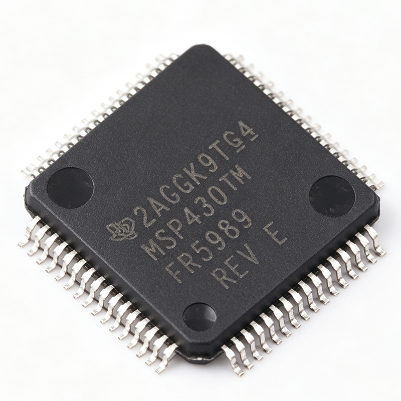
MSP430FR5989IPMR - 128KB FRAM 16MHz Rotary Sensing MCU | TI
The Texas Instruments MSP430FR5989IPMR is a 16-bit ultra-low-power microcontroller based on the MSP430 CPUXV2 RISC core running at up to 16MHz, with 128KB embedded FRAM, 2KB SRAM, and an extended Scan Interface 2 for rotary sensing, housed in a 64-pin LQFP (PM) 10x10mm package. A microcontroller (MCU) is a compact integrated circuit that combines a processor core, program memory, data memory, and programmable peripherals on a single die to govern a specific embedded function. Within the MCU hierarchy, this device belongs to the MSP430 FRAM family of ultra-low-power (ULP) microcontrollers under the broader MSP430 platform and power-management IC taxonomy. Its FRAM (ferroelectric RAM) memory unites SRAM-like speed, flexibility, and endurance with flash-like non-volatility at much lower write energy, eliminating the erase-before-write cycles of conventional flash. Key features include the extended Scan Interface 2 that offloads high-resolution rotary and linear position sensing from the CPU, a hardware AES accelerator for secure metering data, a real-time clock with calendar mode, a 12-bit ADC, comparator, DMA controller, a 32-bit hardware multiplier, and multiple 16-bit timers. Power performance is exceptional: active mode draws approximately 100 uA/MHz and standby (LPM3 with VLO) about 0.4 uA, enabling decade-class battery life in field instruments. Architecturally, the CPUXV2 core executes a 16-bit RISC instruction set over a von Neumann bus at 16MHz. FRAM is byte-writable in-system, allowing fast data logging without external EEPROM, while the AES accelerator encrypts measurements for smart-grid and flow-metering security. The operating supply range is 1.8V to 3.6V with -40C to +85C temperature tolerance for harsh deployments. Typical applications include gas, water, and heat flow meters, rotary and linear position sensing systems, smart-grid endpoints, industrial process control, and secure wireless sensor nodes. Scan Interface 2 directly supports rotary encoders while the CPU sleeps, minimizing average current. Design tip: decouple each VCC pin with 100nF close to the pin plus 10uF bulk capacitance, keep the supply above the SVS threshold for reliable FRAM writes, and use JTAG or two-wire Spy-Bi-Wire for debugging. This page synthesizes distributor pricing, drop-in alternatives, and practical design notes not found in the manufacturer datasheet.
MSP430FR5994 - 16MHz 256KB FRAM MCU with LEA | TI
The Texas Instruments MSP430FR5994 is a 16-bit ultra-low-power microcontroller operating at up to 16 MHz, with 256KB of non-volatile FRAM memory, 8KB of SRAM, a Low-Energy Accelerator (LEA) coprocessor for DSP-style math, and a 64-pin LQFP (10x10 mm) package option. A microcontroller (MCU) is a single-chip embedded computer combining a processor core, memory, and peripherals. The MSP430FR5994 belongs to the 16-bit MCU class, within the broader family of microcontrollers and embedded processors, and sits in TI's MSP430 FRAM platform - a product line that replaces flash memory with ferroelectric RAM for faster, lower-power, and far more durable writes in a unified non-volatile memory architecture. Key differentiating features include the LEA (Low-Energy Accelerator), which TI states delivers up to 40x the DSP performance of Arm Cortex-M0+ class cores for functions such as FFT, FIR filtering, and matrix multiplication, without requiring DSP expertise. The 256KB FRAM supports memory writes at very low energy compared to flash, and the device integrates a 12-bit ADC, comparator, DMA, AES accelerator, and UART/SPI/I2C serial interfaces, plus multiple 16-bit timers. Architecturally, the MSP430FR5994 uses the MSP430 CPUXV2 16-bit RISC core, a hallmark of the lowest-power MCU technology platform on the market. The unified FRAM memory allows code and data to coexist in non-volatile storage, enabling in-application software updates and rapid data logging. Typical applications include battery-powered metering, portable medical and sensor-monitoring equipment, industrial sensing nodes, and edge signal-processing tasks where LEA-accelerated FFT and FIR computation offloads the main CPU. A key design consideration: FRAM writes consume far less energy than flash programming, but designers should still manage the unified memory map carefully when partitioning persistent data segments. This page synthesizes distributor availability data, same-family drop-in alternatives, and practical design notes not found in the manufacturer datasheet.
MSP430FR59941IPM - 16MHz 256KB FRAM MCU | TI
The Texas Instruments MSP430FR59941IPM is a 16-bit MSP430FR FRAM microcontroller running at up to 16 MHz with 256KB non-volatile FRAM, 8KB SRAM, and a Low-Energy Accelerator (LEA) DSP coprocessor, housed in a 64-pin LQFP (PM) package measuring 10x10 mm and rated from -40C to +85C. A FRAM (Ferroelectric RAM) microcontroller is a class of mixed-signal MCU that replaces conventional flash program memory with ferroelectric memory, a technology that combines the non-volatility of flash with the write speed and endurance of SRAM. Within the power-management hierarchy of embedded systems, the MCU sits at the center of the signal chain, controlling sensors, interfaces, and power modes; FRAM MCUs occupy the low-power embedded processing tier, below application processors and above simple 8-bit controllers. Key differentiating features include 256KB of FRAM unified memory with unlimited write endurance in practice and uniform 128-byte write granularity, the LEA hardware accelerator that offloads vector math such as FFTs and FIR filters from the CPU at a fraction of the energy, a hardware AES256 cryptographic accelerator, and a 12-bit SAR ADC. The peripheral set also includes comparators, DMA, four eUSCI serial interfaces (UART/SPI/I2C), and 68 I/O lines made available through TI's port mapping architecture. Architecturally, the device uses the MSP430 CPUXV2 RISC core with 16-bit instructions, a flexible clock system (VLO, REFO, DCO, and external LFXT/HFXT sources), and multiple low-power modes (LPM0-LPM4.5) that let the MCU spend most of its life in sub-microamp sleep states. The FRAM write mechanism requires no erase cycle, so data logging writes are roughly 100x faster and far lower energy than flash-based writes. Typical applications include battery-powered metering and data logging, portable medical monitoring, sensor-fusion nodes performing DSP pre-processing via LEA, and secure connected endpoints using the AES256 engine. Designers should note that FRAM read timing is fast but the maximum system frequency of 16 MHz requires wait-state management for FRAM access above 8 MHz, and the LQFP-64 PM package needs a solid DVSS/DVCC decoupling network per TI's layout guidance. This page synthesizes distributor pricing, same-family drop-in alternatives, pinout guidance, and practical design notes not consolidated in the manufacturer datasheet.
MSP430FR59941IZVWR - 16MHz 256KB FRAM MCU 87-NFBGA | Texas Instruments
The Texas Instruments MSP430FR59941IZVWR is a 16-bit MSP430FR59xx FRAM microcontroller running at 16 MHz with 256KB of FRAM nonvolatile memory, 8KB of SRAM, and a hardware Low-Energy Accelerator (LEA) for digital signal processing, housed in an 87-pin NFBGA (ZVW) 6x6 mm ball grid array package. It integrates a 12-bit ADC, comparator, DMA controller, AES cryptographic accelerator, and up to 68 general-purpose I/O lines with eUSCI serial communication modules. A FRAM (ferroelectric random access memory) microcontroller is a class of MCU in which program flash is replaced by ferroelectric memory, a technology that combines the nonvolatility of flash with the write speed, endurance, and ultra-low write energy of RAM. Within the power management hierarchy of embedded systems, FRAM MCUs occupy the extreme low-power end, enabling energy harvesting and battery designs that conventional flash MCUs cannot match. Key features include the LEA vector math accelerator, which offloads FFT, FIR, and matrix operations from the CPU at a fraction of the energy, and the AES256 accelerator for secure IoT deployments. FRAM writes at full 16 MHz speed with 10^15 cycle endurance, eliminating flash erase-before-write delays and enabling in-system data logging. Operating voltage spans 1.8V to 3.6V with active-mode currents in the microampere-per-MHz class and multiple low-power modes (LPM3.5/4.5) for battery designs. The CPUXV2 16-bit RISC core executes MSP430 instructions with a modernized pipeline. Peripherals include four eUSCI modules supporting UART, SPI, and I2C, a 12-channel DMA, a real-time clock, and a flexible clock system with DCO, LFXT, and HFXT sources. Typical applications include battery-powered metering, portable medical monitoring, energy harvesting sensor nodes, and secure IoT edge devices requiring cryptographic key storage and long battery life. Design consideration: the 87-NFBGA (0.8 mm ball pitch, 6x6 mm) demands careful PCB stack-up; escape routing typically requires a dedicated inner signal layer, and X-ray inspection is recommended for assembly. This page adds distributor pricing, drop-in alternative analysis, and layout guidance not found in the TI datasheet.
MSP430FR59941REV - 16MHz 256KB FRAM MCU with LEA | TI
The Texas Instruments MSP430FR59941REV is a 16-bit MSP430FR microcontroller (MCU) built on the MSP430 CPUXV2 core, running at up to 16 MHz with 256KB of non-volatile FRAM, 8KB of SRAM, and an integrated Low-Energy Accelerator (LEA) for digital signal processing. The device integrates AES hardware acceleration, a 12-bit ADC, comparators, DMA, 68 general-purpose I/O pins, and multiple eUSCI serial interfaces. FRAM (ferroelectric random access memory) is a non-volatile memory technology that combines the speed and low power of SRAM with the endurance and retention of Flash. In the power-management hierarchy, the MSP430FR59941 sits within the MSP430FR599x mixed-signal MCU family, part of TI's ultra-low-power MSP430 portfolio for embedded control and sensing applications. Key differentiating features include the LEA coprocessor, which TI states delivers 40x the signal-processing performance of Arm Cortex-M0+ MCUs for FFT, FIR, and matrix multiplication, without requiring DSP expertise. The 256KB FRAM enables large data logging with unlimited write endurance in practice, while the 12-bit ADC and AES accelerator support secure, precision sensing. Architecturally, the CPUXV2 16-bit RISC core pairs with the LEA vector engine, and FRAM is accessed at full speed, removing the erase-before-write penalties of Flash MCUs. Multiple low-power modes allow active currents in the microamp-per-MHz class, a hallmark of the MSP430 line. Typical applications include smart metering and energy monitoring, industrial sensor front ends with FFT-based analytics, secure IoT sensor nodes using the AES engine, and portable medical devices. Design consideration: FRAM requires no external programming voltage and survives power loss mid-write, but designers should verify the package and pinout details of the REV suffix ordering code directly against the MSP430FR599x datasheet before layout. This page synthesizes verified distributor listings, same-family drop-in alternatives, and practical design notes beyond what a single datasheet page provides.
MSP430FR5994IPMR - 16MHz 256KB FRAM MCU | Texas Instruments
The Texas Instruments MSP430FR5994IPMR is a 16-bit ultra-low-power microcontroller based on the MSP430 CPUXV2 RISC core running at up to 16 MHz, integrating 256KB of FRAM non-volatile memory, 8KB of SRAM, a Low-Energy Accelerator (LEA) DSP engine, an AES256 accelerator, a 12-bit ADC, comparators, DMA, and UART/SPI/I2C serial interfaces in a 64-pin LQFP (10x10 mm, PM suffix) package. A microcontroller (MCU) is a single-chip embedded processor that combines a CPU core, memory, and peripherals on one die, sitting at the device level of the embedded-systems hierarchy (MCU -> embedded processor -> semiconductor). The MSP430FR599x family belongs to the MSP430 FRAM series, which replaces flash with ferroelectric RAM: FRAM offers fast, low-power writes, unified program and data memory, and very high write endurance, making it one of the lowest-power MCU memory technologies available. Key differentiators include the Low-Energy Accelerator (LEA), a hardware signal-processing engine that TI states delivers up to 40x the performance of Arm Cortex-M0+ MCUs on functions such as FFT, FIR filtering, and matrix multiplication, without requiring DSP expertise. The integrated AES256 accelerator secures IoT connectivity, and multiple low-power modes (LPM) extend battery life in always-on sensing applications. Architecturally, the 16-bit CPUXV2 core offloads vector math to LEA via the DMA controller, keeping the CPU in sleep while signal processing proceeds. FRAM is byte-writable with no sector-erase penalty, which simplifies data logging and over-the-air firmware updates. Typical applications include battery-powered sensor nodes, building automation and electronic metering, portable medical devices, and edge signal-conditioning nodes that need FFT/FIR processing at minimal energy cost. Design tip: partition FRAM deliberately - the unified memory allows constants in information segments, but code/data segmentation and write-endurance budgeting should follow TI's FRAM guidance in the MSP430FR599x, MSP430FR596x Mixed-Signal Microcontrollers datasheet (Rev. D). This page adds value beyond the datasheet by synthesizing drop-in alternatives (MSP430FR5989IPMR, MSP430FR59941IPM and related family parts), pricing context as of 2026-09-03, and practical design notes in one place.
MSP430FR5994IPNR - 16MHz 256KB FRAM MCU | Texas Instruments
The Texas Instruments MSP430FR5994IPNR is a 16-bit ultra-low-power FRAM microcontroller running at 16 MHz with 256KB of FRAM nonvolatile memory, 8KB of SRAM, and an integrated Low-Energy Accelerator (LEA) for signal processing, housed in an 80-pin LQFP (12x12 mm) package. FRAM (ferroelectric random access memory) is a nonvolatile memory technology that combines the speed and low power of SRAM-like writes with the data retention of flash. In a microcontroller system hierarchy, the MSP430FR5994 sits within the broader family of mixed-signal MCUs, occupying the memory-and-signal-processing tier of the MSP430FR599x series, which targets battery-powered and energy-harvesting applications that require both large nonvolatile memory and mathematical computation. Key differentiating features include the LEA (Low-Energy Accelerator), a vector math coprocessor that offloads FFT, FIR, and matrix operations from the CPU while the core remains in a low-power state; hardware AES cryptography for secure data handling; a 12-bit ADC and analog comparator for sensing front ends; and direct memory access (DMA) for peripheral-to-memory transfers without CPU intervention. FRAM offers 100x faster writes than flash with inherently low write energy and virtually unlimited write endurance. Architecturally, the MSP430 CPUXV2 16-bit RISC core is paired with multiple low-power modes, enabling active currents in the microamp-per-MHz class while retaining RAM and peripheral state. The unified FRAM memory allows flexible partitioning between code and data, and the MPU (memory protection unit) can segment FRAM into protected regions for bootloader and data-logging designs. Typical applications include portable medical and health monitoring devices, building and factory sensor nodes, energy metering front ends, and battery-powered signal processing where the LEA accelerates FFT-based vibration or acoustic analysis. A key design consideration is the FRAM write protection scheme: configure the MPU segments early in development to prevent accidental data corruption, and respect the maximum operating frequency versus supply voltage relationship documented in the manufacturer datasheet. This page synthesizes distributor pricing, same-family drop-in alternatives, and practical design notes not found in the manufacturer datasheet.

MSP430FR5994IRGZR - 16MHz 256KB FRAM MCU | TI | Low Power
The Texas Instruments MSP430FR5994IRGZR is a 16-bit RISC microcontroller based on the MSP430 CPUXV2 core running at 16 MHz, featuring 256KB of unified FRAM memory, 8KB of SRAM, and a Low-Energy Accelerator (LEA) for signal processing, housed in a 48-pin VQFN (7x7 mm) package. A microcontroller (MCU) is a single integrated circuit that combines a processor core, memory, and programmable peripherals into one chip, forming the lowest layer of the embedded-systems hierarchy: semiconductor -> microcontroller -> embedded system. The MSP430FR5994 belongs to the MSP430 FRAM family of ultra-low-power mixed-signal microcontrollers, where ferroelectric RAM replaces flash to combine non-volatility with fast, low-energy writes. Key differentiating features include FRAM unified memory with 256KB capacity that writes up to 100x faster than flash with far lower energy per byte, the LEA coprocessor delivering up to 40x the DSP performance of Arm Cortex-M0+ cores for FFT, FIR, and matrix operations without requiring DSP expertise, hardware AES encryption, a 12-bit ADC, analog comparators, DMA, and UART/SPI/I2C serial interfaces plus multiple timers. Technically, the FRAM architecture eliminates the erase-before-write penalty of flash, enabling true infinite-endurance data logging and instant software updates. The CPUXV2 16-bit RISC core emphasizes low active power, making the family suitable for battery-powered sensing where every microamp matters. The LEA offloads vector math from the CPU, cutting both execution time and energy per operation in edge signal-processing workloads. Typical applications include portable medical monitoring, industrial sensor nodes, battery-powered metering, and edge signal-conditioning systems that perform FFT or filtering on-chip. The combination of large non-volatile memory and a math accelerator fits data-logging and vibration-sensing designs particularly well. Design consideration: FRAM memory write operations are fast, but code must account for wait states at higher frequencies; use TI's driver library and the MSP430FR599x family datasheet for timing details. This page synthesizes distributor availability, family drop-in alternatives, and practical design guidance not found in a single manufacturer datasheet.
MSP430FR5994IZVW - 16MHz 256KB FRAM MCU, NFBGA-87 | TI
The Texas Instruments MSP430FR5994IZVW is a 16-bit ultra-low-power MSP430 FRAM microcontroller featuring a 16 MHz CPUXV2 RISC core, 256KB of non-volatile FRAM memory, 8KB of SRAM, and an integrated Low-Energy Accelerator (LEA) for digital signal processing, housed in an 87-ball NFBGA (6x6 mm) package. An FRAM (ferroelectric random access memory) microcontroller is a class of mixed-signal MCU that replaces traditional flash program memory with ferroelectric RAM. FRAM offers byte-writable, non-volatile storage with dramatically faster write speeds, near-zero write energy, and essentially unlimited endurance compared to flash, making FRAM MCUs part of the broader power-management-focused, low-power semiconductor hierarchy. The MSP430 family pioneered this category and remains its most widely adopted representative. Key differentiating features of the MSP430FR5994 include the LEA vector coprocessor, which TI states delivers up to 40x the DSP performance of Arm Cortex-M0+ MCUs for functions such as FFT, FIR filtering, and matrix multiplication; hardware AES cryptographic acceleration; a 12-bit SAR ADC; an integrated comparator; a multi-channel DMA controller; and eUSCI serial peripherals supporting UART, SPI, and I2C. Multiple 16-bit timers enable motor control, capture/compare, and PWM applications with very low active and standby power consumption. Architecturally, the device is based on the MSP430 CPUXV2 core with unified FRAM program and data storage, allowing flexible memory partitioning under software control via the Memory Protection Unit (MPU). The LEA offloads block-based DSP math from the CPU, freeing cycles for application logic while operating in low-power modes. Typical applications include battery-powered metering and sensing nodes, industrial sensor front ends requiring FFT-based vibration or acoustic analysis, portable medical monitoring devices, and IoT edge endpoints where ultra-low standby power and long battery life are mandatory. A key design consideration is FRAM write protection: configure the MPU segment boundaries early in development to protect persistent data structures from firmware updates. This page synthesizes distributor pricing, drop-in alternatives, and practical design notes not found in the manufacturer datasheet.
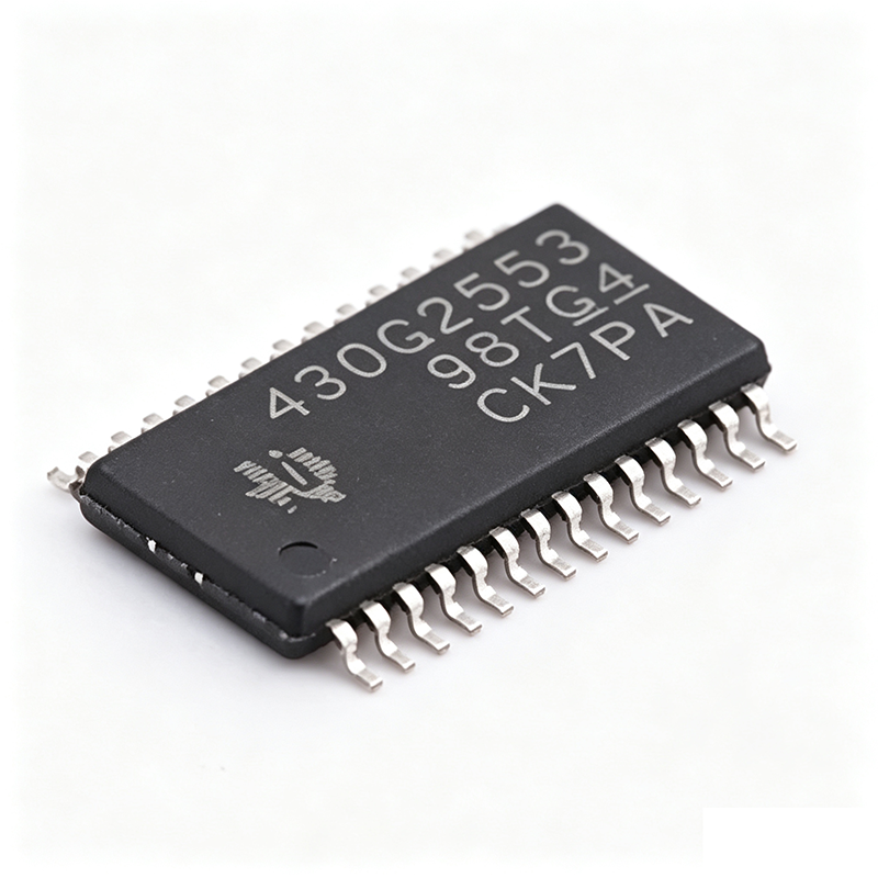
MSP430G2553IPW28R - 16MHz 16KB Flash MCU | Texas Instruments
The Texas Instruments MSP430G2553IPW28R is a 16-bit ultra-low-power mixed-signal microcontroller from the MSP430 Value Line series, featuring a 16MHz CPU, 16KB Flash, 512B SRAM, and a rich set of integrated peripherals. Housed in a 28-pin TSSOP (PW) package, it operates from 1.8V to 3.6V over the industrial temperature range of -40 to +85 C. A microcontroller (MCU) is a compact integrated circuit that governs a specific operation in an embedded system, containing a processor core, memory (Flash and SRAM), and programmable I/O peripherals. The MSP430 family sits within the broader hierarchy of 16-bit RISC microcontrollers under power-management-conscious embedded processing, and is renowned for five low-power modes (LPM0 to LPM4) that reduce current to as low as 0.1 uA in standby mode with RAM retention. Key features include a 10-bit ADC, an analog comparator, two 16-bit timers, and a universal serial communication interface (USCI) supporting UART, SPI, and I2C. The device integrates a temperature sensor, brownout reset, and capacitive-touch-enabled I/O. Its internal DCO is factory-calibrated to 16 MHz with approximately 1% accuracy, often eliminating external crystals. Architecturally, the MSP430G2553 uses a 16-bit RISC CPU with a von-Neumann memory map, enabling efficient code density and rapid wake-up from low-power modes. Firmware can be updated in-system via the two-wire Spy-Bi-Wire interface, simplifying production programming. Typical applications include portable medical devices, wireless sensor nodes, smart meters, remote controls, and battery-powered consumer electronics. The 16KB Flash accommodates substantial application code, while 512B SRAM supports moderate buffering. The integrated comparator and ADC enable direct sensor interfacing, and the multiple communication interfaces allow easy connectivity to radios, displays, and other peripherals. Design tip: place a 0.1 uF capacitor close to DVCC and 1 uF at the power entry; configure unused I/O as outputs to avoid floating-input leakage. This mature, widely available part has extensive community support for both prototyping and production. The MSP430G2553IPW28R is a popular choice for cost-sensitive, power-critical designs where performance and low energy consumption are paramount.
MSP432E401Y - 120MHz Cortex-M4F Ethernet MCU, 1MB Flash | TI
The Texas Instruments MSP432E401Y is a SimpleLink 32-bit Arm Cortex-M4F Ethernet microcontroller running at 120 MHz, with 1 MB (1M x 8) of on-chip flash and 256 kB of SRAM, housed in a 128-TQFP (14 x 14 mm) surface-mount package. A microcontroller (MCU) is a single-chip computer that integrates a processor core, memory, and peripherals into one package. It sits at the heart of the embedded hierarchy: microcontroller unit -> embedded processor -> semiconductor device. The MSP432E401Y belongs to the SimpleLink MCU platform, which spans Wi-Fi, Bluetooth low energy, Sub-1 GHz, Ethernet, Zigbee, Thread, and host MCUs - all sharing a common, easy-to-use development environment with a single core software development kit (SDK) and rich tool set. Key features include the 120 MHz Cortex-M4F core with a hardware floating point unit (FPU) and DSP instructions, 1 MB flash for code storage, 256 kB SRAM for buffers and stacks, and an integrated 10/100 Ethernet MAC and PHY that enables a single-chip networked node without an external PHY. CAN 2.0 support addresses industrial fieldbus requirements. Technically, the MSP432E401Y uses the Arm Cortex-M4F architecture with an advanced interrupt architecture, and its peripheral memory map is shared across the MSP432E4 family as documented in the MSP432E4 Technical Reference Manual (Rev. A). This simplifies software porting between family members and from the legacy TM4C129 series, which is confirmed as pin-to-pin compatible on the TQFP packages per TI E2E forum guidance. Typical applications include industrial Ethernet gateways and IoT nodes, IEEE 1588 PTP precision timing masters, building automation and remote monitoring nodes, and CAN-based industrial control - anywhere cost-sensitive control processing plus wired connectivity is required. The MSP-EXP432E401Y LaunchPad kit provides a fast evaluation path. Design consideration: when migrating from TM4C129x devices, the pinout is pin-to-pin compatible, but software must move to the SimpleLink SDK; TM4C129 MCUs are not part of the SimpleLink family and do not offer its connectivity ecosystem. This page synthesizes distributor pricing, drop-in alternatives, and practical design notes not found in the manufacturer datasheet.

MSPM0G3218-Q1 - 80MHz Cortex-M0+ MCU with CAN-FD | TI
The MSPM0G3218-Q1 is an automotive-grade mixed-signal microcontroller from Texas Instruments, featuring an Arm Cortex-M0+ core running at up to 80 MHz. It is part of the MSPM0G321X family and is designed for automotive applications requiring a CAN-FD interface. According to the TI datasheet, the device integrates a rich set of peripherals suitable for body control, powertrain, and battery management systems. The MSPM0G3218-Q1 is a 32-bit MCU built on the enhanced Arm Cortex-M0+ platform, offering cost-optimized performance with ultra-low power consumption. It operates at up to 80 MHz, providing sufficient processing power for real-time control tasks while maintaining low power sleep modes. The CAN-FD interface enables high-speed data transmission in automotive networks, supporting both classic CAN and CAN-FD protocols. The MCU is supported by the MSPM0 SDK and a hardware ecosystem including LaunchPad development kits, reference designs, and code examples. This ecosystem accelerates development, reducing time-to-market for automotive projects. The device is qualified for automotive applications with AEC-Q100 Grade 1 certification, ensuring robust operation in challenging environments. Key features include the 80 MHz Cortex-M0+ core, CAN-FD interface, and automotive-grade qualification. The MSPM0G3218-Q1 is intended for applications such as body control modules, battery management units, motor control, and sensor interfaces. It provides a flexible GPIO configuration, multiple communication peripherals, and analog signal processing capabilities, making it suitable for mixed-signal control tasks. For design, the MSPM0G3218-Q1 requires careful consideration of power supply decoupling and thermal management. An integrated analog-to-digital converter (ADC) and comparator enable direct interfacing with sensors and actuators. The device supports a wide operating voltage range and includes various low-power modes to extend battery life in automotive systems. The MSPM0G3218-Q1 is a reliable choice for automotive electronics, offering a balance of performance, cost, and low power. Its ecosystem and automotive qualification make it an attractive option for engineers seeking a robust MCU with CAN-FD capability. [DATA_NEEDED: Flash size, RAM size, GPIO count, ADC channels, operating voltage, temperature range]

MSPM0G3507 - 80MHz Cortex-M0+ 128KB MCU CAN-FD | TI
The Texas Instruments MSPM0G3507 is a 32-bit mixed-signal microcontroller based on the enhanced Arm Cortex-M0+ core running at up to 80 MHz, with 128KB flash memory, 32KB SRAM, and an operating supply range of 1.62V to 3.6V across -40C to +125C. It is available in a 48-pin LQFP (7x7 mm) package, with 64-pin LQFP and 32-pin VQFN (5x5 mm, SRHB) options in the same family. A microcontroller (MCU) is a single-chip computer that integrates a processor core, memory, and programmable peripherals such as timers, ADCs, and communication interfaces. Within the semiconductor hierarchy, the MSPM0G3507 belongs to the MSP 32-bit MCU portfolio: MCU -> embedded processor -> integrated circuit. It is a member of the MSPM0G350x performance sub-family, TI's cost-optimized, analog-rich Cortex-M0+ line. Key differentiating features include dual 12-bit ADCs sampling at 4 Msps - unusually fast for the Cortex-M0+ class - a 12-bit DAC, three comparators, and two operational amplifiers that can eliminate external analog front-end components. The MATHACL hardware math accelerator accelerates trigonometric and division operations common in PID and motor-control loops, and the integrated CAN-FD controller supports industrial and automotive networking. Architecturally, the enhanced Cortex-M0+ platform pairs the low-power core with TI's analog peripheral integration and an extended temperature range from -40C to +125C, positioning the MSPM0G3507 between TI's entry-level MSPM0L devices and higher-performance C2000 real-time MCUs. Typical applications include motor control and digital power conversion, industrial sensing and signal-conditioning nodes, CAN-FD networked modules in factory and automotive systems, and medical alarm designs demonstrated in TI's IEC 60601-1-8 reference design using the MSPM0G3507. Design tip: program and debug through the SWDIO/SWCLK pins using an XDS110-based LaunchPad debugger, and use TI SysConfig to configure pins and peripherals graphically. This page synthesizes distributor pricing data, drop-in alternatives within the MSPM0G350x family, and practical design notes not consolidated in the manufacturer datasheet.