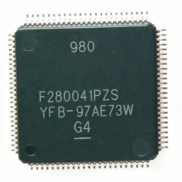
TMS320F243PGE
TMS320F243PGE - 20MHz 16-Bit C24x DSP | Texas Instruments
Texas Instruments TMS320F243PGE is a 16-bit C24x digital signal processor with a 20 MHz clock, 16 KB of flash memory, and a 144-pin LQFP package measuring 20 mm by 20 mm. It belongs to the TMS320C24x family of fixed-point digital signal processors and combines a DSP controller with embedded flash memory for standalone control and signal-processing designs.
A digital signal processor is a specialized microprocessor architecture optimized for arithmetic-intensive operations on continuously sampled or generated signals. The C24x architecture combines a 16-bit fixed-point DSP core with embedded control functions, allowing the same device to implement filters, controllers, communications processing, and motor-control algorithms. Its position in the hierarchy is digital signal processor, then microprocessor, embedded controller, and semiconductor.
The TMS320F243PGE operates from a fixed 5 V supply and executes at 20 MHz. Its 16 KB flash memory is organized as 8K by 16 bits, while the 144-LQFP package exposes the device's digital and analog control interfaces in a surface-mount format. The 20 mm by 20 mm package provides ample routing area for a complex mixed-signal DSP system and is suitable for industrial control boards, instrumentation, communications equipment, and embedded power-conversion systems.
The 16-bit C24x core uses fixed-point arithmetic, making it well suited to digital filters, proportional-integral-derivative control, signal conditioning, and communications algorithms where integer execution speed and deterministic control are important. Embedded flash reduces the need for an external program-memory device in designs that fit entirely within the 16 KB program-memory capacity.
Typical uses include digital power conversion, industrial motor control, measurement and signal-conditioning systems, communications front ends, and compact embedded control platforms. In each case, the device can execute control and signal-processing tasks in one programmable component, reducing the coordination burden associated with separate processor and controller architectures.
PCB design should preserve clean analog and digital return paths, provide local bypass capacitance at the 5 V supply pins, and route high-current or switching outputs separately from sensitive measurement inputs. The 144-pin LQFP footprint requires careful fanout and soldering control, while the 20 MHz operating rate allows conservative clock routing with attention to return-path continuity.
This page organizes the confirmed electrical, memory, package, and sourcing characteristics of the TMS320F243PGE, then adds application guidance, design checks, a same-footprint family alternative, and structured comparisons to support initial component selection and PCB planning.
RFQ
Contact