Power MOSFET Drivers
Products (426)

ADUM4221ARWZ - Isolated Half-Bridge Gate Driver | Analog Devices
The ADUM4221ARWZ is an isolated half-bridge gate driver from Analog Devices, designed to drive high-side and low-side N-channel MOSFETs and IGBTs in power conversion applications. It provides 4 A peak output current with a wide supply voltage range of 2.5 V to 6.5 V on the input side and 4.5 V to 35 V on the output side. The device features adjustable dead time, a disable pin, and a propagation delay of 60 ns, making it suitable for high-frequency switching power supplies, motor drives, and inverters. An isolated gate driver is a specialized IC that provides galvanic isolation between the control circuitry and the power stage, allowing safe and reliable switching of high-voltage power devices. It integrates isolation technology, typically using magnetic or capacitive coupling, to transmit control signals across an isolation barrier while preventing harmful voltage transients from reaching the low-voltage control side. This is essential in applications where the power stage operates at high voltages, such as in industrial motor drives, solar inverters, and electric vehicle chargers. Key features of the ADUM4221ARWZ include a 5 kVrms isolation rating, 100 kV/us common-mode transient immunity (CMTI), and adjustable dead time to prevent shoot-through current. The device also offers a disable pin for output shutdown and a UVLO (undervoltage lockout) function to ensure safe operation during power-up. The 16-lead SOIC package (SOIC-16) provides a compact solution for space-constrained designs. Technically, the ADUM4221ARWZ uses Analog Devices' iCoupler technology, which combines high-speed CMOS and monolithic transformer isolation. This architecture provides reliable signal transfer with low propagation delay and high noise immunity. The device supports both high-side and low-side drive with independent inputs, allowing flexible control of half-bridge topologies. The adjustable dead time, set via an external resistor, enables optimization of switching losses and prevents cross-conduction. Typical applications include isolated switch-mode power supplies (SMPS), motor drives, uninterruptible power supplies (UPS), and photovoltaic inverters. The device's high CMTI and fast propagation delay make it ideal for high-frequency switching circuits where signal integrity is critical. When designing with the ADUM4221ARWZ, ensure proper PCB layout to minimize parasitic inductance and maintain isolation spacing. The input supply should be decoupled with a 0.1 uF capacitor close to the VDD1 pin, and the output supplies should be decoupled with 10 uF electrolytic and 0.1 uF ceramic capacitors. The dead-time resistor should be placed near the DEADTIME pin to minimize noise pickup.
ADUM4221ARWZ-RL7 - Isolated Half-Bridge Gate Driver | Analog Devices
The ADUM4221ARWZ-RL7 is an isolated, half-bridge gate driver from Analog Devices, featuring 4 A peak output current and adjustable dead time. It employs iCoupler technology to provide independent and isolated high-side and low-side outputs, making it ideal for driving power MOSFETs and IGBTs in various power conversion applications. The device is available in a 16-lead SOIC package and operates over a wide supply voltage range. An isolated gate driver is a specialized integrated circuit that provides the necessary voltage and current to switch power transistors while maintaining galvanic isolation between the control side and the power stage. This isolation is critical for safety and noise immunity in applications such as motor drives, switch-mode power supplies, and inverters. The ADUM4221 integrates isolation and drive functions into a single package, eliminating the need for external isolation components like pulse transformers. Key features of the ADUM4221 include 4 A peak output current, adjustable dead time, and a wide supply voltage range. The device supports both high-side and low-side outputs with independent control, enabling flexible half-bridge configurations. Its propagation delay is typically 60 ns, and it offers a common-mode transient immunity of 100 kV/us, ensuring reliable operation in noisy environments. Technically, the ADUM4221 uses Analog Devices' iCoupler technology, which combines high-speed CMOS and monolithic transformer isolation. This architecture provides superior performance compared to traditional optocoupler-based solutions, including lower power consumption, higher data rates, and better timing accuracy. The device also features under-voltage lockout (UVLO) on both the input and output sides, protecting against insufficient supply voltages. Typical applications include isolated switch-mode power supplies, motor drives, solar inverters, and industrial automation. The ADUM4221 is particularly suited for half-bridge and full-bridge topologies where high-side and low-side drivers are required. Its adjustable dead time allows designers to optimize switching performance and prevent shoot-through currents. When designing with the ADUM4221, it is important to ensure proper PCB layout to minimize parasitic inductance and maintain signal integrity. The device's high common-mode transient immunity requires careful attention to grounding and isolation barriers. Additionally, the dead time should be set appropriately based on the switching characteristics of the power transistors to avoid cross-conduction.
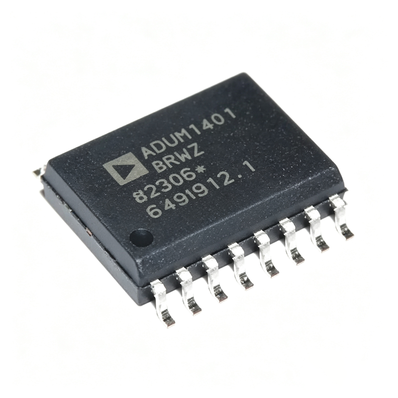
ADUM4221BRWZ - Isolated Half-Bridge Gate Driver | Analog Devices
The ADUM4221BRWZ is an isolated, half-bridge gate driver from Analog Devices, designed to drive high-side and low-side N-channel MOSFETs or IGBTs in power conversion applications. It provides 4 A peak output current and features adjustable dead time, dual inputs, and a wide input supply range of 2.5 V to 6.5 V. The device is housed in a 16-lead SOIC package with a 5 kVrms isolation rating, making it suitable for industrial motor drives, solar inverters, and isolated DC-DC converters. An isolated gate driver is a specialized IC that transfers switching signals across an isolation barrier while providing the high current needed to charge and discharge the gate capacitance of power transistors. It combines galvanic isolation (often via magnetic coupling) with level-shifting and drive circuitry, enabling safe and efficient control of high-voltage power stages from low-voltage control logic. In the hierarchy of power management, it sits between the controller (MCU/DSP) and the power switches, ensuring signal integrity and protecting low-voltage circuitry from high-voltage transients. Key features of the ADUM4221BRWZ include 4 A peak output current, adjustable dead time via an external resistor, and a propagation delay of 60 ns (typical). The device supports a wide output supply range (VDDA/VDDB) from 4.5 V to 18 V, with UVLO thresholds of 7.5 V (typical) for both channels. It also features a disable pin for output shutdown and a CMOS input interface compatible with 2.5 V to 6.5 V logic. The isolation barrier is rated at 5 kVrms for 1 minute, with a working voltage of 560 Vrms, and the device is certified to UL 1577 and IEC 60747-5-5 (VDE 0884-10) standards. Technically, the ADUM4221 uses iCoupler technology, which employs chip-scale transformers to transmit signals across the isolation barrier. This provides reliable operation with high common-mode transient immunity (CMTI) of 100 kV/us, ensuring stable performance in noisy power environments. The adjustable dead time feature allows designers to optimize switching behavior to prevent shoot-through in half-bridge topologies, improving efficiency and reliability. Typical applications include isolated switch-mode power supplies, motor drives, solar inverters, and industrial automation. The device's high output current and fast switching speed make it ideal for driving large MOSFETs and IGBTs in high-power systems. Its wide input supply range and low propagation delay also suit high-frequency switching converters. When designing with the ADUM4221BRWZ, ensure proper PCB layout to minimize parasitic inductance in the gate drive loop, and place the dead-time resistor close to the DT pin. Also, provide adequate decoupling on the output supplies to handle peak currents.
ADUM4221BRWZ-RL7 - Isolated Half-Bridge Gate Driver | Analog Devices
The ADUM4221BRWZ-RL7 is an isolated, half-bridge gate driver from Analog Devices, featuring 4 A peak output current and adjustable dead time. It is based on the iCoupler technology, which combines high-speed CMOS and monolithic transformer isolation to provide robust galvanic isolation up to 3000 Vrms. The device operates from a wide supply voltage range of 2.5 V to 35 V on the high-side and low-side, making it suitable for a variety of power conversion applications. An isolated gate driver is a specialized integrated circuit that provides the necessary voltage and current to drive the gate of power transistors (MOSFETs or IGBTs) while maintaining galvanic isolation between the control side and the power side. This isolation is critical in applications where the power stage operates at high voltages or in noisy environments, as it protects the low-voltage control circuitry and prevents ground loops. The ADUM4221 belongs to the family of isolated gate drivers, which are essential components in switch-mode power supplies, motor drives, and inverters. Key features of the ADUM4221BRWZ-RL7 include a maximum propagation delay of 44 ns, high common-mode transient immunity of 150 kV/µs, and adjustable dead time to prevent shoot-through in half-bridge configurations. The device supports both dual-input and single-input modes (ADUM4221-1 variant) and offers a default low output state for safety. The output rise and fall times are 25 ns, enabling high-frequency switching operation. The ADUM4221 utilizes a proprietary iCoupler transformer-based isolation architecture, which provides superior performance compared to optocouplers or pulse transformers. The isolation barrier is rated for 3000 Vrms, and the device can operate at junction temperatures up to 125°C, making it suitable for demanding industrial environments. The high common-mode transient immunity ensures reliable operation in the presence of fast voltage transients, which is critical in motor drive and inverter applications. Typical applications include isolated switch-mode power supplies, motor drives, solar inverters, and industrial automation. The adjustable dead time feature allows designers to optimize switching efficiency and prevent cross-conduction. The device is available in a 16-lead SOIC package (BRWZ), which is compact and suitable for space-constrained designs. When designing with the ADUM4221, it is important to ensure proper PCB layout to minimize parasitic inductance and maintain signal integrity. The input and output supplies should be decoupled with low-ESR capacitors placed close to the pins. Additionally, the dead time should be set appropriately based on the switching characteristics of the power transistors to avoid shoot-through.
ADUM4222ARWZ - 4A Isolated Half-Bridge Gate Driver | Analog Devices
The ADUM4222ARWZ is a 4 A isolated, half-bridge gate driver from Analog Devices, employing iCoupler technology to provide independent and isolated high-side and low-side outputs. It offers 5000 V rms isolation in a wide-body 16-lead SOIC package, making it suitable for driving IGBTs and MOSFETs in high-voltage applications. The device features 4 A peak output current, a wide supply voltage range, and high-speed CMOS inputs, ensuring reliable switching performance. An isolated gate driver is a specialized IC that transmits control signals across an isolation barrier to drive power transistors in half-bridge or full-bridge configurations. It combines galvanic isolation with high-current drive capability, enabling safe and efficient control of high-voltage power stages. In the hierarchy of power management, it sits between the controller and the power switches, providing level shifting, isolation, and current amplification. Key features include 4 A peak output current, 5000 V rms isolation, 100 kV/us common-mode transient immunity, and a wide operating temperature range. The device supports both high-side and low-side outputs with independent inputs, allowing flexible control of half-bridge topologies. Its propagation delay is typically 50 ns, enabling high-frequency switching. The ADUM4222ARWZ uses Analog Devices' iCoupler technology, which integrates micro-transformers and CMOS circuitry to achieve isolation without optocouplers. This results in superior timing accuracy, lower power consumption, and higher reliability compared to traditional isolation methods. The wide-body SOIC package provides excellent creepage and clearance for high-voltage applications. Typical applications include isolated switch-mode power supplies, motor drives, solar inverters, and industrial automation. The device's high output current and fast switching make it ideal for driving large IGBTs and MOSFETs in power conversion systems. When designing with this device, ensure proper PCB layout to minimize parasitic inductance and maintain isolation spacing. Use appropriate gate resistors to control switching speed and reduce EMI.
ADUM4222ARWZ-RL7 - 4A Isolated Half-Bridge Gate Driver | Analog Devices
The ADUM4222ARWZ-RL7 is a 4 A isolated, half-bridge gate driver from Analog Devices, Inc., employing iCoupler technology to provide independent and isolated high-side and low-side outputs. It is designed to drive power MOSFETs and IGBTs in a wide range of power conversion applications, offering robust isolation and high-speed switching performance. An isolated gate driver is a specialized integrated circuit that provides the necessary voltage and current to switch power transistors while maintaining galvanic isolation between the control side and the power stage. This isolation is critical for safety and noise immunity in applications such as motor drives, switch-mode power supplies, and inverters. The ADUM4222ARWZ-RL7 integrates the isolation barrier and driver circuitry in a single package, simplifying design and improving reliability compared to discrete optocoupler-based solutions. Key features include 4 A peak output current, 5000 Vrms isolation voltage, and a wide supply voltage range. The device supports high-side and low-side outputs with independent inputs, enabling flexible control of half-bridge topologies. It also features a high common-mode transient immunity (CMTI) of 100 kV/µs, ensuring reliable operation in noisy environments. The propagation delay is typically 60 ns, and the device operates over a temperature range of -40°C to +125°C. The ADUM4222ARWZ-RL7 uses Analog Devices' iCoupler technology, which combines high-speed CMOS and monolithic air core transformer technology. This architecture provides superior performance compared to optocouplers, including higher data rates, lower power consumption, and better timing accuracy. The device is available in a 16-lead SOIC package, making it suitable for space-constrained designs. Typical applications include isolated switch-mode power supplies, motor drives, solar inverters, and industrial automation. The device is also suitable for automotive applications, with automotive-grade variants available. When designing with this device, ensure proper PCB layout to minimize parasitic inductance and maintain isolation creepage distances.
ADUM4223ARWZ - 4A Isolated Half-Bridge Gate Driver | Analog Devices
The ADUM4223ARWZ is a 4 A isolated, half-bridge gate driver from Analog Devices that employs iCoupler technology to provide independent and isolated high-side and low-side outputs. It is available in a 16-lead SOIC package and offers 5000 Vrms isolation, making it suitable for high-voltage power conversion applications. The device features two isolated channels, each capable of driving up to 4 A peak output current, with a wide supply voltage range of 3.0 V to 5.5 V on the input side and up to 35 V on the output side. The propagation delay is typically 38 ns, and the device supports high-frequency switching up to 1 MHz, making it ideal for switch-mode power supplies, motor drives, and isolated DC-DC converters. An isolated gate driver is a specialized integrated circuit that provides the necessary voltage and current to drive the gate of a power transistor (such as a MOSFET or IGBT) while maintaining galvanic isolation between the control side and the power side. This isolation is critical in applications where the power stage operates at high voltages or where ground potential differences exist, preventing noise and protecting low-voltage control circuitry. The ADUM4223ARWZ uses magnetic coupling (iCoupler) instead of optocouplers, offering faster propagation delays, better timing accuracy, and higher reliability over temperature and lifetime. Key features of the ADUM4223ARWZ include 4 A peak output current, 5000 Vrms isolation voltage, 38 ns propagation delay, and a wide operating temperature range of -40°C to +125°C. The device also features under-voltage lockout (UVLO) on both input and output supplies, ensuring safe operation during power-up and brown-out conditions. The iCoupler technology provides excellent common-mode transient immunity (CMTI) of 100 kV/us, which is essential for robust operation in noisy industrial environments. The ADUM4223ARWZ is designed for high-performance isolated power conversion. Its architecture integrates a high-speed CMOS interface with monolithic transformer technology, eliminating the need for external components such as pulse transformers or optocouplers. The device supports both high-side and low-side drive with independent inputs, allowing flexible control of half-bridge topologies. The output stage can source and sink 4 A, enabling fast switching of large gate capacitances. Typical applications include isolated switch-mode power supplies (SMPS), motor drives, solar inverters, and industrial power systems. The device is also suitable for automotive applications when using the AEC-Q100 qualified variant (ADUM4223WCRWZ). The high isolation rating and fast propagation delay make it ideal for high-frequency power converters where efficiency and reliability are paramount. When designing with the ADUM4223ARWZ, ensure proper PCB layout to minimize parasitic inductance and maintain isolation spacing. The input and output supplies should be decoupled with low-ESR ceramic capacitors placed close to the pins. The device's UVLO feature helps prevent insufficient gate drive during startup, but designers should verify that the supply voltages meet the UVLO thresholds under all conditions.
ADUM4223ARWZ-RL7 - 4A Isolated Half-Bridge Gate Driver | Analog Devices
The ADUM4223ARWZ-RL7 is a 4 A isolated, half-bridge gate driver from Analog Devices, employing iCoupler technology to provide independent and isolated high-side and low-side outputs. It offers 5000 Vrms isolation in a wide-body 16-lead SOIC package, making it suitable for high-voltage power conversion applications. The device features two isolated channels, each capable of driving up to 4 A peak output current, with propagation delay of 60 ns and minimum pulse width of 50 ns. It operates from a supply voltage range of 2.5 V to 6.5 V on the input side and 4.5 V to 35 V on the output side, with a maximum switching frequency of 1 MHz. The ADUM4223ARWZ-RL7 is designed for robust performance in industrial, automotive, and renewable energy systems, providing reliable gate drive for IGBTs and MOSFETs in half-bridge and full-bridge topologies. An isolated gate driver is a specialized integrated circuit that provides the necessary voltage and current to switch power transistors while maintaining galvanic isolation between the control side and the power stage. This isolation is critical for safety and noise immunity in high-voltage systems, preventing ground loops and protecting low-voltage control circuitry. The ADUM4223ARWZ-RL7 uses magnetic coupling (iCoupler) instead of optocouplers, offering superior speed, reliability, and temperature stability. It fits within the broader category of gate drivers, which are essential components in power electronics, bridging the gap between microcontrollers and high-power switches. Key features include 4 A peak output current, 5000 Vrms isolation, 60 ns propagation delay, and 50 ns minimum pulse width. The device also features under-voltage lockout (UVLO) on both input and output supplies, ensuring safe operation during power-up and brown-out conditions. The wide-body SOIC-16 package provides excellent creepage and clearance distances for high-voltage applications, and the device is rated for operation from -40°C to +125°C. Technically, the ADUM4223ARWZ-RL7 integrates high-speed CMOS and monolithic transformer technology, achieving performance superior to pulse transformer and gate driver combinations. The iCoupler technology ensures precise timing and low jitter, which is critical for high-frequency switching. The device supports both high-side and low-side drive with independent inputs, allowing flexible control of half-bridge configurations. The output stage is designed to drive large capacitive loads, such as the gate capacitance of power MOSFETs and IGBTs, with minimal delay and distortion. Typical applications include isolated DC-DC converters, motor drives, solar inverters, and uninterruptible power supplies (UPS). In these systems, the ADUM4223ARWZ-RL7 provides reliable gate drive with high noise immunity, enabling efficient and safe power conversion. Its wide supply range and robust isolation make it a versatile choice for both industrial and automotive power electronics. When designing with this device, ensure proper PCB layout to maintain isolation spacing and minimize parasitic inductance. Use appropriate decoupling capacitors on both supply pins, and consider the thermal performance of the package under high-frequency operation. The UVLO thresholds should be matched to the system's power-up sequence to avoid unintended switching.
ADUM4224ARWZ - 4A Isolated Half-Bridge Driver | Analog Devices
The ADUM4224ARWZ is a 4A isolated precision half-bridge gate driver from Analog Devices, utilizing iCoupler technology to provide independent and isolated high-side and low-side outputs. It offers 5000Vrms isolation in a 16-pin SOIC package, making it suitable for a wide range of power conversion applications. An isolated gate driver is a device that transfers control signals across an isolation barrier to drive power transistors such as MOSFETs and IGBTs. It ensures safety and noise immunity by galvanically isolating the low-voltage control side from the high-voltage power stage. This is essential in applications like motor drives, inverters, and switch-mode power supplies where high voltages and transients are present. Key features include 4A peak output current, 5000Vrms isolation voltage, and a wide supply voltage range. The device supports both high-side and low-side driving with independent inputs, enabling flexible half-bridge configurations. It also features a UVLO (undervoltage lockout) on both supplies to ensure safe operation during power-up and brownout conditions. Technically, the ADUM4224ARWZ uses Analog Devices' proprietary iCoupler technology, which integrates micro-transformers to achieve isolation. This provides superior performance compared to optocouplers, including higher data rates, lower power consumption, and better timing accuracy. The driver has a propagation delay of [DATA_NEEDED: propagation delay] and a minimum pulse width of [DATA_NEEDED: minimum pulse width], ensuring precise switching. Typical applications include isolated switch-mode power supplies, motor drives, solar inverters, and industrial automation. The device is well-suited for driving power MOSFETs and IGBTs in half-bridge or full-bridge topologies, where its high output current ensures fast switching and reduced switching losses. When designing with the ADUM4224ARWZ, ensure proper decoupling of the VDD1 and VDD2 supplies with low-ESR capacitors. Also, consider the isolation rating and creepage distances for the PCB layout to maintain the specified isolation voltage.
ADUM4224ARWZ-RL7 - 4A Isolated Half-Bridge Driver | Analog Devices
The ADUM4224ARWZ-RL7 is a 4 A isolated, half-bridge gate driver from Analog Devices, employing iCoupler technology to provide independent and isolated high-side and low-side outputs. It offers 5000 V rms isolation in a wide-body, 16-lead SOIC package, making it suitable for high-voltage applications where galvanic isolation is critical. The device is designed to drive power MOSFETs and IGBTs in half-bridge and full-bridge configurations, delivering robust gate drive with fast propagation delays and high common-mode transient immunity. An isolated gate driver is a specialized integrated circuit that transfers control signals across an isolation barrier to drive the gate of a power transistor while maintaining electrical isolation between the low-voltage control side and the high-voltage power side. This isolation protects sensitive control electronics from high-voltage transients and ground loops, and is essential in applications such as motor drives, power inverters, and switch-mode power supplies. The ADUM4224 belongs to the family of digital isolators and gate drivers, which are critical components in modern power electronics. Key features of the ADUM4224 include 4 A peak output current, 5000 V rms isolation voltage, and a wide supply voltage range from 4.5 V to 18 V on the output side. The device supports a logic input voltage range of 2.7 V to 5.5 V, making it compatible with a variety of microcontrollers and digital controllers. It also features a dead-time control input, allowing precise timing of high-side and low-side switching to prevent shoot-through current. The propagation delay is typically 60 ns, and the common-mode transient immunity is 100 kV/us, ensuring reliable operation in noisy environments. The ADUM4224 uses Analog Devices' iCoupler technology, which integrates micro-transformers and high-speed CMOS circuits to achieve isolation and signal transfer. This architecture provides superior performance compared to optocoupler-based drivers, including higher speed, lower power consumption, and better reliability. The wide-body SOIC-16 package offers excellent creepage and clearance distances, meeting stringent safety standards for industrial and automotive applications. Typical applications include isolated switch-mode power supplies, motor drives, solar inverters, and electric vehicle charging systems. The device is also suitable for industrial automation and robotics, where high-voltage isolation and robust gate drive are required. Its high output current and fast switching speed make it ideal for driving large power MOSFETs and IGBTs in high-frequency power converters. When designing with the ADUM4224, it is important to provide adequate decoupling on both the input and output supply pins, and to minimize parasitic inductance in the gate drive loop. The dead-time control pin should be configured to match the switching characteristics of the power transistors to avoid cross-conduction. Proper PCB layout with sufficient copper area for heat dissipation is recommended for high-current applications.

AUIPS7091GTR - 1.5A Automotive High-Side Switch | Infineon
The Infineon AUIPS7091GTR is an automotive-grade intelligent power high-side switch delivering up to 1.5 A continuous output current from a 6 V to 35 V supply rail, housed in an 8-pin PG-DSO-8 surface-mount package. The device integrates a single N-channel MOSFET driver with 100 mOhm typical on-resistance, active-low enable input, diagnostic current sense output, and comprehensive on-chip protection including over-current, over-temperature, over-voltage, and reverse-battery protection. As a member of Infineon's AUIPS (Automotive Intelligent Power Switch) family, it is qualified for harsh automotive 12 V/24 V load environments and supports load-dump tolerant operation up to 35 V. A high-side switch is a power-distribution topology in which the switching element sits between the positive supply rail and the load, allowing the load to be connected to chassis ground and enabling ground-referenced diagnostics. Compared with low-side switching, the high-side architecture protects downstream wiring and electronics from short circuits to ground, eliminates ground-shift issues, and allows multiple loads to share a common ground. The AUIPS7091GTR belongs to the broader category of intelligent power switches (IPS), also called eFuses or solid-state relays, which combine a power MOSFET, gate driver, and protection logic in a single IC. Key features include a 1.5 A continuous current rating, 100 mOhm typical Rds(on) at 25 C, 5.5 V minimum operating supply, fast output slew-rate control for EMI reduction, and an analog current-sense pin proportional to load current. Internal protections include load-current limitation, junction thermal shutdown with auto-restart, active over-voltage clamping at Vov, and reverse-battery robustness without external components. The PG-DSO-8 package has an exposed thermal pad for low theta-JA and is qualified to MSL2 floor life of 1 year at 30 C / 60% RH. Architecturally, the AUIPS7091GTR combines a vertical N-channel DMOS output stage with CMOS control logic and an on-chip charge pump that generates the gate drive above Vbat. The current-mirror sense technique produces a small analog voltage at the IS pin that is proportional to the load current, enabling closed-loop diagnostics without a shunt resistor. Compared with electromechanical relays, this topology provides silent switching, microsecond actuation, and immunity to contact wear and bounce. Typical applications include automotive body-electronics loads such as solenoids, valve actuators, relay replacement, LED driver modules, and small motor control. It is also used in industrial PLC outputs and 24 V truck / bus load management where 35 V load-dump survivability is required. When designing with the AUIPS7091GTR, place a low-ESR ceramic decoupling capacitor close to Vbat and route the IS pin trace away from switching nodes to avoid capacitive coupling. The diagnostic current sense requires an external pull-up resistor to a logic rail; choose the resistor to keep the sense voltage within the ADC input range. This page synthesizes distributor pricing, drop-in alternatives, and practical design notes not found in the manufacturer datasheet, providing engineers a single reference for sourcing and design-in.

AUIR3242STRXUMA1 - High-Side MOSFET Driver | Infineon
The Infineon AUIR3242STRXUMA1 is an automotive-grade high-side MOSFET driver IC in a PG-DSO-8-907 (8-pin SOIC) package, designed for back-to-back MOSFET switch topology. The device operates from 3V to 36V, integrating a boost DC/DC converter that uses an external inductor to generate gate-drive voltage above the battery rail, enabling standard-level N-channel MOSFETs to be driven even at low battery conditions. It features a non-inverting input control and very low quiescent current in both ON and OFF states, making it suited for always-on automotive loads. A high-side MOSFET driver is a specialized gate-driver IC that switches the gate of an N-channel MOSFET referenced to the positive supply rail rather than ground. This topology simplifies low-side wiring, reduces ground-loop noise, and protects downstream loads from ground-shift faults. The AUIR3242S family belongs to a broader hierarchy of gate drivers within Infineon's automotive power-management portfolio, sitting alongside half-bridge and bootstrap-based high-side drivers. Key features include reverse-battery protection, very low quiescent current, internal boost converter, and automotive-grade qualification per Infineon's reliability standards. The non-inverting logic input makes relay replacement straightforward, and the wide 3V-36V input range covers 12V and 24V automotive buses with load-dump margin. The PG-DSO-8-907 surface-mount package offers compact footprint and good thermal performance for under-hood PCB layouts. The driver combines a charge-pump/boost converter using a small external inductor with a gate-driver output stage. The boost topology generates VGS above VIN, ensuring full enhancement of standard N-channel MOSFETs even when battery voltage sags during cranking. Reverse-battery protection blocks destructive current flow if the supply polarity is reversed during service or jump-start events. Typical applications include back-to-back N-channel MOSFET switches in automotive body modules, battery isolation switches, eFuse replacements, relay replacement circuits, and load-driving in BCM (body control modules). The low Iq enables permanent connection to battery without significant quiescent drain, satisfying modern vehicle quiescent-current budgets. Designers should select an external inductor and bootstrap/charge-pump capacitor per the datasheet's typical-application circuit to ensure stable boost operation. Reverse-battery protection eliminates the need for an external blocking diode in most 12V systems, reducing BOM count and board area. The input control pin can be driven directly from a microcontroller GPIO or a logic-level signal.
AUIRS21811STR - 600V Half-Bridge Gate Driver 1.9A | Infineon
The Infineon AUIRS21811STR is a 600 V half-bridge gate driver IC housed in an 8-pin SOIC (SO-8) package with 1.9 A peak source / 2.3 A peak sink drive current and a non-inverting logic input. The part operates from a 10 V to 20 V VCC supply, tolerates negative transient voltages on the bootstrap high-side rail, and is qualified to AEC-Q100 for automotive environments. A gate driver IC is a power-management semiconductor that translates low-power PWM control signals from a microcontroller or DSP into the high-current gate-drive signals required to switch discrete power MOSFETs, IGBTs, or GaN FETs. Gate drivers sit between the logic controller and the power stage in the system hierarchy: gate driver -> power management IC -> semiconductor -> discrete switch. By providing local high-current drive and level-shifting, they reduce switching losses, allow smaller gate resistors, and protect the controller from high-voltage transients on the switched node. Key features of the AUIRS21811STR include 1.9 A source / 2.3 A sink peak output current, 600 V absolute maximum bootstrap high-side rail, 10 V to 20 V VCC range with integrated undervoltage lockout (UVLO) on both VCC and VBS rails, 60 ns typical rise time and 35 ns typical fall time into a 1 nF load, and 160 ns propagation delay (typical). The 8-SOIC footprint keeps the design compact while the high dV/dt immunity and negative VS transient tolerance simplify layout in half-bridge and full-bridge motor-drive topologies. Architecturally, the AUIRS21811STR uses a level-shifted high-side channel with a floating bootstrap supply referenced to the switch node (VS), allowing continuous high-side drive up to the 600 V rail. The low-side channel is supplied directly from VCC. The input stage accepts 3.3 V/5 V CMOS or logic-level inputs with non-inverting polarity, and the matched propagation delays between channels simplify dead-time control in complementary PWM applications. AEC-Q100 grade-1 qualification and automotive-grade moisture sensitivity level (MSL3) make it suitable for underhood and chassis electronics. Typical applications for the AUIRS21811STR include automotive 12 V/48 V motor drives (HVAC blowers, oil/water pumps, electric power steering auxiliary rails), DC-DC converter primary-side MOSFET driving, Class D audio amplifiers, and small industrial half-bridge inverters. The wide bootstrap tolerance also makes it usable in 230 V AC PFC and totempole PFC front ends when the topology calls for a 600 V driver. When designing with this part, place the VCC bypass capacitor (typically 0.1 uF ceramic in parallel with 10 uF bulk) as close to pins 5 and 8 as possible, and keep the bootstrap diode and BST capacitor (typically 0.1 uF to 1 uF) loop tight to limit the high-side rail ringing. For applications above 1 kW per phase, verify that the 1.9 A source/2.3 A sink rating gives sufficient gate-charge headroom for the chosen MOSFET/IGBT; larger switches may require a dedicated gate-driver buffer stage. This page synthesizes distributor pricing, drop-in alternatives, and practical design notes that supplement the manufacturer datasheet and help engineers select, source, and lay out the AUIRS21811STR with confidence.

BSP742RIXUMA1 - 400mA Smart High-Side Switch 41V | Infineon
The Infineon BSP742RIXUMA1 is a single-channel smart high-side power switch from the miniPROFET family, rated at 400 mA continuous output current and 41 V load dump capability, housed in a PG-DSO-8-6 (standard SOIC-8, 3.90 mm body width) surface-mount package. The device integrates a vertical N-channel power MOSFET, embedded protective functions, and a diagnostic feedback pin, making it a one-chip replacement for discrete MOSFET plus discrete protection circuitry. A smart high-side power switch is a semiconductor device that connects a load to the positive supply rail and integrates an N-channel MOSFET with comprehensive on-chip protection (overload, short-circuit, thermal shutdown, overvoltage including load dump, and reverse battery protection on most variants) plus status diagnostics. Within the broader taxonomy, this part sits in: smart power switch -> high-side switch -> power distribution IC -> PMIC -> power management -> semiconductor. The miniPROFET family specifically targets 12 V automotive and industrial loads such as lamps, solenoids, relays, and small motors where PCB area and reliability are critical. Key features include 250 mΩ typical on-state resistance (RDS(on)) at 25°C, current limitation set internally at approximately 0.4 A continuous load, thermal shutdown with automatic restart, fast demagnetization of inductive loads, and reverse battery protection rated to -16 V. The diagnostic pin reports open-load and overtemperature conditions. Operating supply range spans 5 V to 34 V (with 41 V load-dump transient tolerance), covering standard 12 V automotive rails with full margin. Architecturally the device combines a vertical DMOS output stage, charge pump for gate drive, bandgap-derived references, and an analog sense chain for current-limit and temperature monitoring. Integrated protection eliminates the need for a freewheeling diode across inductive loads because the same die absorbs the demagnetization energy internally. Typical applications include 12 V automotive body electronics (door lock actuators, mirror heaters, lamp drivers up to 400 mA), industrial PLC outputs, and any 12 V/24 V subsystem needing protected high-side switching with status feedback to a microcontroller. Companion products typically include a small microcontroller for diagnostic decoding and a flyback-resilient supply such as IFX007TAUMA1 or BTS462TATMA1 for higher-current rails. Design tip: derate the continuous current to approximately 0.3 A in a sealed enclosure without forced airflow; sustained 0.4 A operation requires the exposed pad to be soldered to at least 1 cm² of copper pour on the PCB. Inputs above 16 V continuous should be avoided on reverse-battery-tolerant variants. This page synthesizes distributor pricing, drop-in alternatives, design considerations, and parametric comparison data not found in the standalone manufacturer datasheet — useful for engineers evaluating BSP742RIXUMA1 in 12 V/24 V high-side load-switch designs.
BSP742RXUMA1 - 400mA Smart High-Side Switch, 5-34V | Infineon
The Infineon BSP742RXUMA1 is a 400 mA smart high-side power switch built around an integrated vertical N-channel power FET, housed in a PG-DSO-8-6 (8-pin small-outline) surface-mount package. It is a member of Infineon's Classic PROFET 12V family and is qualified to AEC-Q100 for automotive 12V load management, supporting an operating voltage range of 5 V to 34 V with a typical on-resistance of 70 mΩ. A high-side power switch is a semiconductor device that connects a load to the positive supply rail and controls current flow through the load using an N-channel MOSFET placed between the supply and the load. Within the broader component taxonomy, the BSP742RXUMA1 sits in the PMIC (Power Management IC) category as a power distribution switch / load driver, distinct from low-side switches (which sit between load and ground) and from DC-DC converters (which actively regulate voltage). High-side switches are preferred in automotive body electronics because they safely disconnect the load from the battery in fault conditions and prevent dangerous "load on ground" situations. Key specifications include 400 mA continuous load current, 70 mΩ typical R_DS(on) at 25°C, embedded protection features (overload, short-circuit, thermal shutdown with auto-restart, overvoltage including load-dump, and reverse-battery protection), and CMOS-compatible logic inputs with both active-high and active-low versions. The device also integrates fast demagnetization of inductive loads, making it ideal for driving relays, solenoids, valves, and small motors without external freewheeling diodes. The BSP742RXUMA1 uses Infineon's vertical DMOS process with charge-pump gate drive to deliver a true high-side switch in a compact 8-pin SO package. Its diagnostic feedback output reports fault status back to the microcontroller, supporting ISO 26262-style functional-safety architectures. The wide 5 V to 34 V operating range covers automotive cranking transients and 24 V truck/bus systems, while the low 5 µA quiescent current minimizes parasitic battery drain. Typical applications include automotive body electronics (door modules, seat control, mirror heaters), 24V industrial automation loads, programmable logic controller (PLC) digital outputs, and any 12V/24V load-driving circuit requiring embedded protection. The device is pin-to-pin compatible with other members of the Infineon PROFET family such as BSP742R, allowing designers to scale current per channel without PCB rework. When designing with this device, observe the maximum junction temperature of 150°C and derate load current aggressively above 85°C ambient. The input pins accept 3.3V or 5V CMOS logic directly; tie the input pin to Vbb through a pull-up resistor if left floating to prevent unwanted turn-on. Always place a reverse-polarity protection diode or use the part's internal reverse-battery feature with proper heat-sinking. This page synthesizes real-time distributor pricing, drop-in compatible pin-to-pin alternatives from the Infineon Classic PROFET family and key competitors, and practical PCB/protection design notes that go beyond the manufacturer datasheet's typical application circuit.

BSP752RXUMA2 - 1.3A Smart High-Side Power Switch | Infineon
The Infineon BSP752RXUMA2 is a 1.3 A smart high-side N-channel power switch with integrated vertical DMOS FET and embedded protection, housed in a PG-DSO-8-6 (DSO-8-6) surface-mount package. It is part of Infineon's miniPROFET family and provides a single-channel 1:1 power switch/load driver architecture with on-state resistance in the 100-200 milliohm range, operating across an automotive/industrial supply envelope suitable for 12 V vehicle rails. The device includes built-in diagnostic feedback and protections that turn a discrete MOSFET, sense resistor, fuse, and protection circuitry into one IC. What is a high-side power switch? A high-side power switch sits between the supply rail (e.g., +12 V battery) and the load, replacing mechanical relays and discrete MOSFETs. The category hierarchy is: high-side switch -> load driver -> power distribution switch -> power management IC. By placing the switch on the high side, the load is grounded, simplifying wiring harnesses and improving short-circuit behavior versus low-side switching. Key features include 1.3 A continuous load current capability, integrated overload protection with active current limitation, short-circuit protection, thermal shutdown with auto-restart, overvoltage protection including load-dump transients, fast demagnetization of inductive loads, reverse-battery protection, and an open-load detection in the OFF state through an external resistor. The status feedback pin reports fault conditions to the microcontroller. According to the Infineon datasheet, the device operates over the automotive -40C to +150C junction temperature range and is qualified to AEC-Q100 standards for automotive environments. Architecturally, the BSP752RXUMA2 combines a vertical N-channel DMOS output stage with CMOS control logic, charge pump for gate enhancement, and bandgap-referenced protection comparators. The charge pump maintains VGS above threshold even at low supply voltages, while the protection comparators monitor drain current, junction temperature, and supply voltage independently and act within microseconds to safeguard the FET. Typical applications include automotive body electronics (door modules, seat controllers, mirror adjusters, interior lighting), industrial 24 V load driving, PLC digital outputs, and any application replacing an automotive relay or fuse-protected discrete MOSFET high-side path. The DSO-8-6 footprint is footprint-compatible with other miniPROFET family members for design reuse. When designing with this part, observe the maximum junction temperature of 150C and provide adequate copper pour on the PG-DSO-8-6 exposed pad for thermal dissipation. Choose external pull-up/pull-down values per the diagnostic pin's specified current to ensure reliable logic levels across temperature. This page synthesizes distributor pricing tiers, drop-in miniPROFET alternatives sourced from Infineon's product family and cross-brand parametric equivalents, and design notes not consolidated in any single manufacturer document.
BSP762TXUMA1 - 2A Smart High-Side Power Switch | Infineon
The Infineon BSP762TXUMA1 is a 2 A smart high-side N-channel power switch in a PG-DSO-8-6 (DSO-8) surface-mount package, belonging to Infineon's MINI-PROFET family of protected single-channel high-side switches. It integrates a power MOSFET, charge pump, and comprehensive protection circuitry to drive resistive, capacitive, and inductive loads directly from microcontroller I/O lines. A high-side power switch is a type of power distribution switch that sits between the positive supply rail and the load, providing controlled ON/OFF switching plus diagnostic feedback. In the broader product hierarchy, it belongs to power management ICs, specifically the power distribution switch / load driver category, and complements LDO regulators, DC-DC converters, and eFuse ICs by providing a robust, self-protected interface to the load. Key features of the BSP762TXUMA1 include a 2 A continuous load current capability, integrated reverse battery, overcurrent, short-circuit, over-temperature, overvoltage, and undervoltage lockout protection. The device operates over a -40 C to +150 C junction temperature range and includes load-dump protection suitable for 12 V automotive environments. Its integrated charge pump drives the internal N-channel MOSFET, achieving low Rds(on) without an external gate drive supply. The BSP762TXUMA1 implements a 1:1 power switch/driver architecture with a single input control pin and an open-drain status feedback pin for fault reporting. The PG-DSO-8-6 thermally-enhanced package provides a low thermal resistance path from the die to the PCB copper pour, enabling 2 A operation without an external heatsink in typical PCB layouts. Typical applications include 12 V automotive body electronics such as LED lighting drivers, solenoid and relay replacement circuits, small motor drivers, and resistive heating loads. It is also used in industrial PLC digital outputs and consumer white-goods appliance controls where MCU-driven high-side switching replaces mechanical relays. When designing with this part, ensure the PCB copper pour provides adequate heatsinking for the chosen load current. Place a 100 nF ceramic bypass capacitor close to the supply pin, and respect the diagnostic pin pull-up voltage limits to avoid damage during reverse-battery transients. This page synthesizes distributor pricing, drop-in alternatives, and practical design notes not found in the manufacturer datasheet, delivering actionable information for design engineers and procurement teams evaluating the BSP762TXUMA1.
BSP772TXUMA1 - 2.6A Smart High-Side Power Switch | Infineon
The Infineon BSP772TXUMA1 is a 2.6 A smart high-side N-channel power switch housed in a PG-DSO-8-6 (8-pin SOIC with exposed pad) package, part of Infineon's Classic PROFET family. It integrates a single 1:1 power MOSFET with built-in protection, status feedback, and diagnostic features, delivering a monolithic load-driver solution that replaces discrete MOSFET + fuse + protection circuits. The device is specified for 2.6 A continuous load current and targets 12 V automotive and industrial rails. A high-side power switch (also called a smart high-side switch, high-side load driver, or PROFET) is a semiconductor device that sits between the positive supply rail and the load. Unlike a low-side switch that returns current to ground, a high-side switch allows ground-referenced loads (lamps, solenoids, motors) to be turned on and off without disturbing the load's reference. Smart variants integrate protection and diagnostics; the BSP772TXUMA1 belongs to the Classic PROFET subfamily, sitting within the broader category of power distribution switches -> PMIC -> power management IC -> semiconductor. Key features include over-current protection, over-voltage clamp, over-temperature shutdown, ESD protection, short-circuit protection, and an open-drain status flag pin for fault feedback to a microcontroller. The integrated charge pump drives the N-channel MOSFET gate, achieving low typical on-state resistance which minimizes conduction losses and thermal stress. The PROFET family is widely adopted in body electronics modules for driving lamps, motors, solenoids, and resistive heaters. Technically the device combines a vertical N-channel DMOS output stage with CMOS/BCD control logic on a single die. The integrated reverse-battery protection and ground-loss robustness allow direct connection to the 12 V automotive bus without external reverse-polarity components. The 8-pin SOIC with thermal pad (PG-DSO-8-6) provides low thermal resistance for dissipating load current losses in compact PCB areas. Typical applications include automotive body electronics (interior lighting, door modules, seat controllers), industrial 24 V/12 V load driving, relay replacement, and protected power distribution in PLC and HVAC systems. The device is also used in motorcycle and e-bike ECUs and as a protected USB VBUS switch in automotive head units. When designing with the BSP772TXUMA1, ensure input capacitance is placed close to the supply pin and that the tab/exposed pad is soldered to a sufficient copper pour for heat dissipation. The status pin requires an external pull-up resistor; the input (IN) pin is TTL/CMOS compatible. Avoid continuous operation at maximum current above 25C ambient unless proper thermal management is applied. This page consolidates distributor pricing, drop-in alternatives (including same-brand Classic PROFET siblings and cross-brand equivalents), and practical design notes not found in the standalone manufacturer datasheet.

BSP77E6433HUMA1 - 42V 2.17A Smart Low-Side Switch | Infineon
The Infineon BSP77E6433HUMA1 is a 42 V N-channel power FET packaged in a 4-pin (3+Tab) SOT-223 (PG-SOT223-4) surface-mount package, designed as an automotive-grade smart low-side switch with integrated ESD and overload protection. It belongs to Infineon's Classic HITFET™ 12 V family and is rated for a continuous drain current of approximately 2.17 A with logic-level gate drive, making it ideal for 12 V DC systems in vehicles. The device combines a vertical N-channel MOSFET with monolithic protection circuitry, replacing discrete MOSFET plus discrete driver designs with a single protected switch. A low-side switch is a semiconductor power switch placed between the load and ground, in contrast to a high-side switch placed between the supply and the load. Low-side switches are widely used for cost-sensitive, ground-referenced loads such as solenoids, relays, lamps, heaters, and small DC motors where the wiring return path can tolerate being switched. Within the broader semiconductor taxonomy, the BSP77 sits in the hierarchy: low-side switch → power distribution switch → load driver → power management IC → semiconductor. Infineon's HITFET family adds integrated protection features—overload, overtemperature, ESD, and active current limiting—that discrete N-channel MOSFETs require external circuitry to provide. Key features include a 42 V drain-to-source breakdown voltage providing substantial transient headroom above 12 V automotive rails, an active current limit, thermal shutdown with auto-restart, and ESD protection on the input pin. The logic-level input accepts standard 3.3 V or 5 V microcontroller GPIO signals directly, simplifying firmware-driven load control. The 4-pin SOT-223 (PG-SOT223-4) footprint exposes the drain tab for both electrical connection and thermal dissipation, with a low junction-to-ambient thermal resistance that supports sustained 2.17 A operation on minimum copper area. Architecturally, the BSP77 uses Infineon's Smart SIPMOS technology, integrating a vertical N-channel DMOS output stage with CMOS-compatible control logic and bandgap-referenced protection comparators on a single die. This co-integration allows the protection thresholds to track the output MOSFET's safe operating area, giving precise overload and short-circuit behavior across temperature. The monolithic approach reduces parasitic inductance compared to discrete solutions, improving switching performance and EMC. Typical applications include automotive body electronics such as LED drivers, small motor control (window lifters, mirror adjusters, door locks), relay and solenoid replacement, resistive heating elements (seat heaters), and general 12 V load switching in industrial 24 V systems with adequate derating. The integrated protection makes it especially suitable for applications where load faults (short to battery, stuck relay contacts) must not damage the ECU. When designing with this device, observe the Safe Operating Area in the manufacturer datasheet and ensure the tab is soldered to a copper area sized for the worst-case dissipation. Bypass the input pin with a 100 nF ceramic capacitor placed close to the IC to suppress ESD-induced transients. For inductive loads, add a freewheeling diode; the BSP77 does not include internal avalanche clamping for inductive turn-off. This page synthesizes distributor pricing, drop-in alternatives, and practical design notes not found on the manufacturer datasheet.

BSP78HUMA1 - 42V 3A Smart Low-Side Switch | Infineon HITFET
The Infineon BSP78HUMA1 is a 42V, 3A N-channel vertical power FET implemented in Smart SIPMOS technology, packaged in a PG-SOT223-4 surface-mount outline and qualified to AEC-Q100 for automotive use. It functions as a self-protected low-side switch integrating a logic-level input, ESD protection, overload protection, short-circuit protection, overvoltage protection (including load-dump transients), current limitation, and thermal shutdown with auto-restart. Maximum on-state resistance is 200 mΩ typical at room temperature, with a continuous load current capability up to 3 A. The integrated charge pump holds the gate above threshold during low-Vds operation, ensuring stable Rds(on) across the full operating range. A low-side switch is a power switch that connects the load to ground while the high side of the load sits at the supply rail. Compared with high-side switches, low-side drivers simplify N-channel MOSFET drive because the source reference is at ground, but they cannot detect load-side ground faults and they share the chassis/board ground with the controller. BSP78HUMA1 belongs to the broader HITFET family of Infineon protected switches - devices positioned between discrete MOSFETs (which require external protection) and full high-side PROFET switches, and they serve automotive body-electronics, industrial 24 V systems, and any application that needs a robust, logic-controlled ground-referenced switch. Key features include 4.5 V to 42 V operating supply range, logic-level input compatible with 3.3 V and 5 V microcontrollers, open-drain diagnostic output for fault feedback, very low standby current, and -40 °C to +150 °C operating junction temperature. The PG-SOT223-4 (TO-261-4) package with an exposed tab provides a low thermal resistance path to PCB copper, supporting sustained 3 A switching without external heatsinking in well-designed layouts. Typical applications span automotive body controllers driving resistive, inductive, or lamp loads, industrial PLC outputs, 24 V solenoid and valve drivers, LED lighting modules, and any 12 V/24 V ground-referenced load that benefits from on-die protection. The device is drop-in compatible with the broader Infineon HITFET family in the same SOT-223 footprint. When designing with the BSP78HUMA1, ensure the inductive load has a freewheeling path (clamp diode or TVS) and that the PCB tab is soldered to a sufficient copper pour to keep junction temperature within SOA. The diagnostic pin requires a pull-up resistor; floating it disables fault reporting. This page consolidates distributor pricing, parametric cross-reference alternatives, and design notes that complement the manufacturer datasheet for engineers evaluating a 12 V/24 V protected low-side switch.

BTF3050TEATMA1 - 3A 12V HITFET+ Low-Side Switch | Infineon
The Infineon BTF3050TEATMA1 is a 3 A N-channel low-side power switch from Infineon's HITFET+ family, housed in a PG-TO252-5-11 (DPAK-5) surface-mount package. It integrates an N-channel MOSFET power stage with 3.3 V/5 V CMOS-compatible logic inputs, on-chip ESD protection, current limiting, and adjustable switching slew rate for 12 V automotive and industrial loads. The device is qualified to AEC-Q100 for automotive use and supports an operating supply range of 3.0 V to 5.5 V on the logic supply and continuous drain current up to 3 A. A low-side switch (also called a low-side driver) is a type of power distribution switch that places an N-channel MOSFET between the load and ground, with the load tied directly to the supply rail. This topology is widely used in automotive body electronics, where it offers simple logic-level control, inherent short-to-ground protection, and easy paralleling of multiple channels. Low-side switches sit in the broader power-management hierarchy of load drivers -> power distribution switches -> power management ICs -> semiconductors, and are a complement to high-side switches such as Infineon's PROFET family. Key differentiating features of the BTF3050TEATMA1 include a 100 mOhm maximum on-state resistance (RDS(on)) at 25 C, an adjustable dV/dt slew-rate pin for EMI tuning, a 30 A internal current limit, status feedback, and a typical turn-on time of 15 us with turn-off of 30 us. Protection features include over-current, over-temperature, over-voltage, and reverse-battery ruggedness, making it suitable for harsh 12 V automotive environments where load-dump transients are common. The BTF3050TE uses a vertical N-channel MOSFET output structure with charge pump gate drive, allowing full enhancement at logic-level VGS. The integrated charge pump, ESD network and protective diodes are co-packaged in the same die as the power MOSFET, enabling a compact 5-pin DPAK footprint. This monolithic integration reduces external component count compared to discrete MOSFET + driver designs. Typical applications include driving automotive solenoids, relays, lamps, LED strings, small DC motors, and resistive heating elements. It is also widely used as a protected driver for industrial PLC outputs and process-control valves. The PG-TO252-5-11 (DPAK) package has a low thermal resistance (RthJA around 50 C/W on a 1 sq inch copper pour), supporting continuous 3 A operation with proper PCB thermal design. When designing with this part, ensure the PCB copper area under the tab is sufficient to dissipate I^2RDS(on) losses at worst-case ambient temperature. A 10 nF gate capacitor on the SR pin is the typical starting point for slew-rate adjustment, but the value must be tuned to the load's inductance to avoid ringing below the EMI limit. This page synthesizes distributor pricing, drop-in alternatives, and practical design notes not found in the manufacturer datasheet, with all parametric values cross-checked against the Infineon HITFET+ datasheet.

BTG70013A1ESWXUMA2 - 26.6A PROFET Wire Guard 12V High-Side Switch
The Infineon BTG70013A1ESWXUMA2 is a 26.6 A single-channel smart high-side power switch in the PROFET Wire Guard 12V family, housed in a PG-TSDSO-24-32 package with exposed pad. It integrates a vertical N-channel power MOSFET with 1:1 power switch/driver logic, on-chip protection, and digital diagnostics targeted at 12 V automotive and industrial body-electronic loads. The device operates from a nominal 12 V supply, supports load currents up to 26.6 A, and is qualified to ISO 26262 for safety-related automotive systems. A high-side switch is a power-distribution building block that sits between the supply rail (typically the automotive 12 V battery) and the load, replacing discrete fuses, relays, and MOSFET drivers. It belongs to the broader category of smart power switches (also called intelligent power switches, IPS, or PROFET devices), which integrate a power transistor, gate driver, current sense, and diagnostic feedback into one IC. Within a vehicle electrical/electronic (E/E) architecture, it sits under the body control module (BCM) and power distribution box, protecting wiring harnesses from over-current and short-circuit events while reporting fault status back to the MCU. Key specifications of the BTG70013A1ESWXUMA2 include a 26.6 A maximum load current, an active-high logic input, a selectable integrated I²t wire-harness protection function, an IDL pin for microcontroller wake-up from key-off mode, and an operating supply current under 60 µA in active key-off (idle) mode. Embedded protection features include over-current, over-voltage, over-temperature, reverse battery, and loss-of-ground protection per Infineon's PROFET datasheet. The device is rated for use with 12 V automotive loads and supports diagnostic feedback through a status / current-sense pin. The BTG70013A uses a vertical DMOS output stage driven by a charge-pump-assisted gate driver, enabling true rail-to-rail low-RDS(on) switching in a small PG-TSDSO-24-32 thermal-enhanced package. The integrated I²t characteristic lets designers select a wire-protection curve by external component choice, matching the thermal limit of the harness rather than a fixed silicon trip point. This is critical for AEC-Q100 and ISO 26262-compliant automotive wiring systems where the wire itself is the weakest thermal element. Typical applications include automotive body-electronic loads such as LED lighting modules, seat heaters, mirror heaters, auxiliary 12 V outlets, and small DC motor drivers. It is also used in industrial 24 V systems and truck / agricultural 24 V body controllers where 12 V-class smart switches are deployed per channel. The low idle current under 60 µA makes it suitable for permanently-live nodes that must not drain the battery during key-off parking. When designing with this part, ensure the PCB layout provides sufficient copper area on the exposed pad for thermal dissipation, place the input/bulk capacitor as close as possible to the VBB pin, and configure the I²t selection network per the application curve in the datasheet. The IDL wake pin must be wired to an MCU interrupt-capable GPIO to use the key-off wake feature; floating this pin disables the wake function but does not affect normal operation.
BTG7003A1EPWXUMA2 - 15.7A PROFET Wire Guard High-Side Switch | Infineon
The Infineon BTG7003A1EPWXUMA2 is a single-channel, 15.7 A high-side smart power switch from the PROFET™ Wire Guard 12 V family, housed in a PG-TSDSO-14-22 exposed-pad package. Built around an N-channel power MOSFET configured as a 1:1 high-side driver with active-high logic input, the device integrates wire-protection diagnostics (I²t), over-current, over-voltage, and thermal shutdown, and is qualified to ISO 26262 for use in automotive safety-relevant systems. Continuous load current is rated up to 15.7 A with a low 50 µA idle-mode quiescent current, making it suitable for energy-efficient body and chassis ECUs. A high-side switch (HSS) is a semiconductor load driver that sits between the supply rail (e.g., a 12 V automotive bus) and the load, controlling current return through the device. PROFET Wire Guard is a sub-category of protected MOSFET switches that adds on-die diagnostic and protection logic. This sits inside the broader hierarchy: smart power switch -> load driver -> power management IC -> semiconductor device. PROFET Wire Guard devices are designed specifically for 12 V automotive wiring harnesses, where they can detect and react to wire faults that classic fuses cannot. Key features of the BTG7003A1EPWXUMA2 include an operating voltage range of 6 V to 18 V (load-dump tolerant up to 40 V), 15.7 A continuous load current, 50 µA idle current, integrated I²t wire-protection, reverse-battery protection, and an integrated charge pump that provides true high-side switching with R_DS(on) of about 10 mΩ. The PG-TSDSO-14-22 package has an exposed thermal pad that minimizes junction-to-PCB thermal resistance, allowing the part to sustain high continuous currents in compact modules without an external heatsink. From an architecture standpoint, the device pairs a vertical N-channel power stage with on-die control logic including a charge pump, gate driver, current sense, and protection state machine. The I²t wire-protection algorithm emulates the thermal time constant of the wire harness, allowing the switch to predictably limit energy delivered into a fault before the conductor overheats. Infineon's ISO 26262 documentation streamlines integration into ASIL-rated systems. Typical applications include automotive body-control modules, seat-heater and seat-belt pretensioner drivers, LED lighting drivers, HVAC flap actuators, and generic 12 V resistive or inductive load switching. The device is best suited when designers need a single robust high-side channel rather than a multi-channel PROFET+ device, or where wire-protection certification is required. When designing with this device, ensure the load is truly single-channel and within 15.7 A; for higher current use a parallel PROFET+ part. Add a reverse-battery blocking diode or use the integrated feature, and follow Infineon's PCB layout guidance for the exposed pad. This page synthesizes distributor pricing, drop-in alternatives, and practical design notes not found in the manufacturer datasheet.
BTG70501EPLXUMA1 - 3A Smart High-Side Switch | Infineon PROFET
The Infineon BTG70501EPLXUMA1 is a 3 A automotive smart high-side power switch (PROFET +2 12V Load Guard) housed in a 14-pin PG-TSDSO exposed-pad package. It integrates a 1:1 N-channel power MOSFET driver with built-in current limiting at 3 A, comprehensive diagnostic feedback, and enhanced protection features for 12 V automotive power distribution. The part is qualified to AEC-Q100 for automotive use. A high-side smart switch (PROFET) is a type of power distribution switch that sits between the supply rail (typically a 12 V automotive battery) and the load, replacing discrete MOSFETs plus fuses with a single protected IC. The PROFET family sits inside the broader taxonomy: power distribution switch -> load driver -> power management IC -> semiconductor. Compared with a discrete N-MOSFET driven by a GPIO, a PROFET provides accurate current limiting, short-circuit protection, thermal shutdown, and load-dump immunity in one IC, simplifying PCB layout and improving reliability for body-electronics loads. Key features of the BTG7050-1EPL include a 3 A overcurrent trip, 2.7 V to 28 V supply range (Vcc), -40 C to +150 C junction temperature, current limit switch (CLS) mode for ADAS and power distribution, plus diagnostic outputs that signal open-load, short-to-battery, short-to-ground, and overtemperature events. The exposed-pad PG-TSDSO-14 package keeps the thermal path short for repetitive inrush loads such as LED arrays, solenoids, and small DC motors. The BTG7050-1EPL is built on Infineon's PROFET +2 12V smart-power process, which combines a vertical N-channel DMOS output stage with mixed-signal control logic on the same die. The current-limit loop is trimmed per device, which avoids the unit-to-unit variation seen in discrete polyfuse or PTC solutions and gives predictable behavior at cold-crank (Vbat dropping momentarily below 6 V) and load-dump (Vbat surges above 35 V) events. Typical applications include body-control modules driving LED lighting, relay replacement, seat-heater elements, mirror actuators, and infotainment peripherals. The wide Vcc range and AEC-Q100 qualification make it equally suitable for ADAS sensor rails and zonal-architecture power distribution. CLS mode is specifically tuned for power-distribution topologies where multiple PROFETs feed downstream ECUs. When designing with this part, follow Infineon's recommended PCB layout for the exposed thermal pad - solder the EP to a copper pour of at least 1 cm^2 to keep RthJA within the datasheet envelope under repeated inrush. Always check the inrush profile of the load (bulb, motor, capacitor bank) against the published I(SC) and E(AS) limits before selection. This page synthesizes distributor pricing, drop-in alternatives, and practical design notes that go beyond the manufacturer datasheet, giving procurement and design engineers a single reference for evaluating the BTG70501EPLXUMA1 in 12 V automotive power-distribution designs.